arxiv: v1 [cond-mat.mes-hall] 28 Mar 2011
|
|
|
- Spencer Hoover
- 5 years ago
- Views:
Transcription
1 Electronic structure effects in stability and quantum conductance in 2D gold nanowires Vikas Kashid, 1 Vaishali Shah 2 and H. G. Salunke 3 1 Department of Physics, University of Pune, Pune , India arxiv: v1 [cond-mat.mes-hall] 28 Mar Interdisciplinary School of Scientific Computing, University of Pune, Pune , India 3 Technical Physics Division, Bhabha Atomic Research Center, Mumbai , India Abstract We have investigated the stability and conductivity of unsupported, two dimensional infinite gold nanowires using ab-initio density functional theory (DFT). Two dimensional ribbon like nanowires, with 1-5 rows of gold atoms in the non-periodic direction and with different possible structures have been considered. The nanowires with > 2 rows of atoms exhibit dimerization, similar to finite wires, along the non-periodic direction. Our results show that in these zero thickness nanowires, the parallelogram motif is the most stable. A comparison between parallelogram and rectangular shaped nanowires of increasing width indicates that zero thickness (111) oriented wires have a higher stability over (100). A detailed analysis of the electronic structure, reveals that the (111) oriented structures show increased delocalization of s and p electrons in addition to a stronger delocalization of the d electrons and hence are the most stable. The density of states show that the nanowires are metallic and conducting except for the double zigzag structure, which, is semiconducting. Conductance calculations show transmission for a wide range of energies in all the stable nanowires with more than two rows of atoms. The conductance channels are not purely s and have strong contributions from the d levels and weak contributions from the p levels. 2 Corresponding author. vaishali@unipune.ac.in 1
2 I. INTRODUCTION Structural stability of gold nanowires (NWs) and the resulting effect on conductance is of interest not only from its applicatory value but also for its basic physics studies. Finite size effects, resulting from the thinning of wires, on the structural stability and electronic properties is an interesting topic for study. Yanson et al. 1 and Ohnishi et al. 2 showed experimentally that gold NWs fabricated between the two electrodes during the thinning process transform successively from quadruple to linear strands. The conductance quanta in these NWs changed from 4 to 1 G o (where, G o = 2e 2 /h). They also found that the (111) and (100) atomic sheets had a stable structure and deformation of the atomic sheets lead to an increase in the conductance. Theoretically, a first systematic investigation in NWs of gold was performed by Sanchez-Portal et al., 3,4 where-in, the authors observed that zigzag NWs were more stable than single atomic chains (SAC) and other nano-structures. It is well known from Peirel s argument, 5 that SAC would be less stable than either bi-atomic chains (BAC) or zigzag structures. Hence, zigzag structures contributed a important finding in Sanchez-Portal s paper. More recently, F. Tavazza et al. 6,7 have performed a relatively more detailed theoretical investigation of gold wires under tensile stress and strain. They observed that gold wires elongate to form single atom chains (SAC) just before fracture via a series of intermediate structural transformations. The authors investigated seven structures as a starting point and investigated evolution of these into single atom chains under tensile strain. The authors also observed 2D structures are energetically more favorable than 3D structures. However, this study was limited only to the stability of structures under stress and strain. There are no reports in literature on detailed investigations into the electronic origins of quantum conductance of wires different than linear. Most of the theoretical and experimental investigations published so far are limited largely to structural stability and the measurement of conductance in gold NWs pulled from atomic tips Furthermore most of the investigations are limited to single or double rows of gold NWs. The short length (4-5 atoms) and double row chains have limited potential for practical applications in comparison with somewhat longer atomic chains. A further drawback of investigations performed on NWs suspended in tips is that tips may not be implementable in functional devices. Structural stability of longer NWs under device operating conditions and with respect to the likely atomic processes happening at these temperatures, however 2
3 will play an important role in the integration of NWs in various technologies. In the present paper, we intend to investigate stability of infinitely long gold NWs and concomitant quantum conductance in the wires from a detailed theoretical perspective. We have investigated the stability of two dimensional (2D) ribbon like gold NWs of different shapes with increasing number of rows. Besides the geometrical structure, the electronic structure has been analyzed to understand the correlation between the structure, stability and conductivity in these wires. Our results show that in the nanoregime the electronic contributions have an important role in determining the stability and conductivity of the NWs. We discuss the increased stability of (111) oriented NWs over (100) NWs based on the contributions of p electrons. All previous investigations on conductivity in NWs are limited to measuring the conductance, however, the electronic origins of conductance have not been investigated in detail. We believe, this study will aid further systematic investigations into the effect of different alloying elements on the stability, conductivity and other physical properties of these and similar NWs, an area yet unexplored extensively. Such investigations especially related with NWs composed of magnetic and non-magnetic elements may reveal novel magnetic and conducting properties. The organization of the paper is as follows. In the next section, we describe the technical details of our simulations on the gold NWs. In Sec. III, we describe our results on the geometric structure and discuss the stability of the NWs based on their electronic structure. The correlation between electronic structure and conductivity is discussed in Sec. IV followed by a brief summary of the main results in Sec. V. II. COMPUTATIONAL METHOD We have performed total energy calculations based on ab intio density functional theory (DFT) as implemented in the Vienna ab initio Simulation Package(VASP) The Projector Augmented Wave method (PAW) 18 and Generalized Gradient Approximation (GGA) 19 has been used to describe electron-ion interactions and exchange correlation interactions. The NWs are modeled in a periodically repeated unit cell, whose dimensions are chosen in such a way that the wires are infinite and periodic in the x direction with 12 Å vacuum spacing in y and z directions. A plane-wave energy cut-off of ev (13.2 Ry) was used. The energy convergence of linear wire was tested with respect to the number of k-points 3
4 used for integrating the Brillouin Zone. A mesh of k-points in the Monkhorst Pack scheme gave reasonable convergence in the total energy. The same mesh of k-points has been used for all other structures. Atomic relaxations are performed by conserving the shape and volume of the unit cell. The NW structures have been optimized using the Residual Minimization (RMM-DIIS) 20 method and the Conjugate gradient (CG) 21,22 method. The structural optimizations have been performed until the total forces on individual atoms are less than 0.01 ev/å. The binding energy per atom (E B ) for gold NWs is calculated as E B = [E T ne atom ] n where, E T is the total energy of the NW, E atom is the energy of single gold atom and n is the total number of atoms. In order to understand the electronic and conduction properties of the NWs, we have performed band structure calculations. For the linear wire, the Brillouin zone integration has been performed from Γ(0,0,0) to X(0.5,0,0) direction with 10 equidistant kpoints. Except for the linear wire, all other geometries are two dimensional. Considering this, the two dimensional Brillouin zone has been integrated along Γ(0,0,0) to X(0.5,0.5,0)- direction using 10 equidistant kpoints. In order to understand the contributions of the electrons in the s, p and d states to the energy levels in the band structure, the fat band technique was applied. The technique has been developed and implemented by Jepsen et al. 23 in the LMTO-ASA tight binding method. We have developed a similar technique in VASP by giving a width to the electronic energy band that is proportional to the sum of the corresponding orthonormal orbital(s). The details of the technique of the fat band method with VASP package are described in V. Kashid et al. 24 We have also performed spin polarized DFT calculations for the infinite NW geometries. These calculations show that infinite NWs are non-magnetic in nature. The conducting properties of gold NWs are investigated based on the Landuaer-Büttiker formalism, 25 using the method of plane waves, 26 For each nanowire, the conductance is calculated as G(E) = 2e2 h T (E) where, T(E) is the transmission function at a particular energy and calculated as T (E) = N(E), 4
5 Here, N(E) are number of states. The number of states can be directly obtained from the band structure of the gold NWs. III. RESULTS AND DISCUSSION A. Structure Structural optimizations were performed on fourteen different structures of gold nanowires with 1-5 rows of atoms. Except for the linear (LR) nanowire, all other NWs studied are two dimensional, with increasing number of rows of Au atoms, in one of the non-periodic directions. Amongst 14 unconstrained NW structures we investigated, some structures have been previously reported in the literature. The linear NW has been studied in great detail as free standing 3,4,13,27,28 as well as suspended between tips. 6 8,10,29,30 Unconstrained structures like zigzag (ZZ), rectangular (RT-1), parallelogram (PR-1) and double zigzag (DZZ) structures have also been investigated by other researchers. 3,4,27,29,31 More recently, Tavazza et al. have found that 2D structures like ZZ, PR-1, PR-2, DZZ and centered hexagonal (CHX) are formed intermediately during the thinning process. 7 We optimized all the NW geometries by varying the bond lengths between the gold atoms in the periodic direction. Figure 1 shows the structures of NWs investigated. The structures in Fig. 1 are ordered according to the increasing number of rows of atoms in the 2D NWs and for a particular number of rows, the structures are shown with increasing stability. In Fig. 1, for a given 2D row of atoms, we have nearly exhausted all structural possibilities. For example, in Fig. 1(d), with four rows of atoms, four structural possibilities are applicable. Thus, hexagonal (HX), DZZ, triple rectangle (RT-3) and triple parallelogram (PR-3) structures are investigated. In most of the wires, the optimized structures have been found to have primarily, zigzag, rectangular and parallelogram motifs or their combinations. 1. Single and Double row NWs The single row linear NW shown in Fig. 1(a) is well studied. The possible simplest 2D NW with 2 rows of atoms are shown in Fig. 1(b) viz., zigzag (ZZ), rectangular (RT-1) and parallelogram (PR-1) (referred as zigzag under compression by Portal et al. 3,4 ). We have investigated these wires for verification and completeness of our calculations. Most of the 5
6 literature on linear NW is for the wires suspended between the tips. Linear NW has been found to be highly stable under stretching forces and has a quantum conductance of 1G o at room temperature. 1,2,27,28,32 Our optimized linear wire with an uniform Au-Au bond length of 2.61 Å, is in good agreement with the bond length of 2.60 Å reported by Zarechnaya et al. 33 Unlike finite gold NWs, 34,35 the infinite linear NWs do not show variation in the bond length or dimerization, in agreement with, the calculations by Xiao et al. 34 and Nakamura et al. 27 Our optimized ZZ structure has a bond length of 2.55 Å and bond angle of This agrees very well with the bond angle of 131 calculated by D. Portal et al. 3 Our calculated distance between Au 1 and Au 3 atoms is 4.66 Å, which, compares quite well with 4.62 Å obtained by D. Portal et al. 3 that demonstrate the binding energy plot has two minima as a function of bond angle for the ZZ structure. Our calculations are in confirmation with earlier observations that the ZZ structure is a metastable structure when compared with PR-1 structure. These results were arrived from the binding energy plot as a function of bond angle. 3,4 The ZZ structure is at the higher minimum (-1.90 ev) and the PR-1 structure is at the lower minimum (-2.22 ev) of the binding energy plot. The RT-1 structure has a length of 2.65 Å, width of 2.68 Å and the bond angles of 90. The relativistic calculations by Nakamura et al. 27 have obtained 2.59 Å as the length and width of the rectangular wire. 27 The PR-1 structure, is a more compact structure than the zigzag structure with all acute angles between the gold atoms. The length and width of parallelogram is 2.67 Å and 2.76 Å respectively. An average bond length of 2.76 Å for parallelogram shaped NW has been reported earlier by Tavazza et al. under elastic deformation in between the tips. 7 The bond angle analysis shows that the parallelogram is formed of two isosceles triangles in disagreement with the structure reported by Fioravante et al., 31 which is made up of equilateral triangles. The preference for isosceles triangles over equilateral triangles is on account of symmetry breaking along the non-periodic y direction. The PR-1 structure is found to be the most stable double row NW, in agreement, with the earlier calculations by Portal et al. 3,4 and Nakamura et al. 27 6
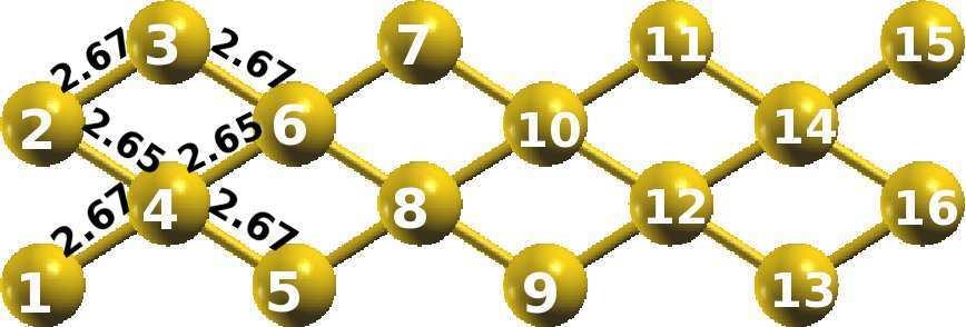
7 2. Triple row NWs We have examined three, triple row NW structures, double rectangular (RT-2), pentagonal (PNT), and double parallelogram (PR-2) as shown in Fig. 1(c). We have also performed optimization of another three row geometry, i.e., the rhombus structure (not shown in the figure). We find that further lattice optimization of the infinite length rhombus structure leads to the energetically lower PR-2 structure. Unlike the ZZ structure, which has a distinct minima in the binding energy versus lattice separation diagram, the rhombus structure does not reside in a distinct potential well. The optimization path smoothly curves down to the PR-2 structure. Recently, a single rhombus structure held between parallelogram NWs on both sides was observed as an intermediate structure during compression of linear NW. 7 However, we would like to note that, so far, there have been no experimental reports of two dimensional rhombus shaped NW. 29 The RT-2 structure, is made up of uniform rectangles stacked one on top of another, with a length of 2.70 Å, and width of 2.62 Å. The initial geometry set up for the PNT NW was made up of regular pentagons. Geometry optimization of this regular structure lead to a structure that has an admix of a RT-1 NW and a PR-1 NW as shown in Fig. 1c (ii). The horizontal bond length is enhanced by 0.05 Å and 0.03 Å in comparison with their equivalent bond lengths in RT-1 and PR-1 structures respectively. The diagonal bond length in PNT is reduced by 0.02 Å in comparison with PR-1 structure. The bond angles between Au 2 -Au 5 -Au 4 and Au 2 -Au 4 -Au 5 are 60.5 and 59.0 respectively. The corresponding angles in the PR-1 structure are 61.2 and 57.6, respectively. The PR-2 structure is the most stable three row geometry. In the PR-2 NW, Au 1 -Au 2 have a bond length of 2.74 Å and Au 2 -Au 5 have a bond length 2.80 Å. The bond angles between Au 1 -Au 2 -Au 6 and Au 2 -Au 6 -Au 1 are 61.4 and 60.3 respectively. Our analysis of bond angles shows that PR-2 structure is comprised of slightly distorted equivalent triangles. 3. Quadruple row NWs Fig. 1(d) shows the four row NW structures considered, namely, hexagonal (HX), double zigzag (DZZ), triple rectangular (RT-3), and triple parallelogram (PR-3). The optimized HX structure has bond lengths between Au 1 -Au 2, Au 2 -Au 3 and Au 2 -Au 15 as 2.58 Å, 2.58 Å, 7
8 and 2.69 Å respectively. The structure is a slightly distorted hexagon with bond angles of and The DZZ structure is made up of two zigzag NWs, with one placed on top of another one. The bond lengths between the atoms forming the zigzag shape, Au 1 -Au 4, Au 2 -Au 3, Au 4 -Au 5, Au 3 -Au 6 are 2.67 Å. The bond lengths between the atoms Au 2 -Au 4, Au 4 -Au 6 are 2.65 Å. Bond angle between Au 1 -Au 4 -Au 2 is 65.4, whereas, the bond angle between the atoms Au 1 -Au 4 -Au 5 is In the DZZ structure, the bond lengths have stretched by 0.12 Å in comparison with the ZZ structure and the bond angles have reduced. The RT-3 wire is interesting, as, it is the first NW geometry that exhibits dimerization in the y direction. Although dimerization in finite linear wires is well observed and reported, 34 dimerization in thicker wires has not been reported so far. The length of the rectangles in RT-3 NW is 2.68 Å. The widths of the top, middle and bottom rectangles are 2.65 Å, 2.61 Å and 2.65 Å, respectively. The dimerization has been explained on the basis of non-uniform potential experienced by the atoms in the finite length direction. No dimerization is observed in the infinite length direction in gold NWs on account of every atom experiencing a uniform potential. 27,34 The PR-3 structure is formed of parallelograms that have a uniform length of 2.72 Å. The widths of the two terminal parallelograms are 2.75 Å, which have expanded by 0.01 Å in comparison with the PR-2 NW. The width of the central parallelograms is 2.74 Å, same, as that of the PR-2 NW. 4. Quintuple row NWs We have investigated three, five row NW structures, centered hexagonal (CHX), quadruple rectangular (RT-4) and quadruple parallelogram (PR-4) as shown in Fig.1(e). The CHX wire is generated from the HX wire (shown in Fig. 1d (i)) by placing a gold atom at the center of each hexagon. The additional atom in the center, expands the length of each side of hexagon by 0.12 Å. The bond angles are observed to expand in one case from to 118.3, while the other contracts from to in comparison with that of the HX NWs. The RT-4 structure shows dimerization in the non-periodic direction like the RT-3 NW. The terminal rectangles have a width of 2.66 Å and the two central rectangles have a width of 2.63 Å. The terminal and central rectangles have a uniform length of 2.66 Å. The PR-4 structure is made up of slightly distorted equilateral triangles. The length of the 8
9 parallelograms is 2.73 Å. The width of the terminal parallelograms is 2.76 Å whereas, that of the two central parallelograms is 2.74 Å. Similar to the RT-4 NW, dimerization in the length along the non-periodic direction is observed. In general, as the number of rows in the NW increases, the bond lengths between the gold atoms along the length of the NW are seen to increase, whereas, the bond lengths perpendicular to the length decrease. Linear NW has the smallest bond length (2.61 Å) and the PR-4 has the largest bond lengths (2.73 Å). This bond length is smaller by 0.22 Å in comparison with the bulk bond length of 2.95 Å. The bond angles show an opposite trend. The bond angles are decreasing with an increasing number of rows in the NWs. In the PR shaped NW s, the bond angles are converging with increasing number of rows to their bulk value of 60. Within a particular number of rows, the bond lengths of the less stable NW structures are smaller than the bond lengths of the most stable NWs. Similar to finite gold NWs, 34 dimerization along the finite second dimension of the wire, is observed in RT-3, PR-3, RT-4 and PR-4 NWs. We would like to note that the structure of RT-3 and RT-4 wires is similar to zero thickness nanoribbon of (100) surface and that of PR-3 and PR-4 wires is similar to a zero thickness nanoribbon of (111) surface. B. Stability The stability of linear wires has been investigated earlier by Nakamura et al. 27 and Portal et al. 3 Their calculations have shown that the PR-1 shaped wire is more stable over the ZZ and RT-1 wires. These three NWs are made up of a double row of atoms and have a higher stability in comparison with the LR wire. The stability of the ZZ wire over the LR wire is argued to be on account of the d levels in the ZZ NWs being situated well below the Fermi level, in comparison with, that of the LR wire. This raises a few interesting questions related with zero thickness NWs. Will the stability of the NWs increase as one increases the width i.e. the number of rows in the 2D NWs? Is stability related to the location of the d levels with respect to the Fermi level? In order to investigate this, we have listed the NWs in ascending order of stability in Table I. The number of atomic rows in the non-periodic direction are also listed. In agreement with the earlier calculations, 3 we observe that the LR wire is less stable. The ZZ NW is stable over linear NW by 0.2 ev and the PR-1 wire is stable over ZZ and RT-1 wire by
10 ev and 0.13 ev, respectively. In the three row NW structures, the PR-2 wire is more stable over the RT-2 and PNT wires by 0.15 ev and 0.07 ev, respectively. In the four row structures, the DZZ is stable by 0.31 ev in comparison with the HX NWs. This DZZ NW has been considered to be a magic structure adopted by NWs during the thinning process. 31 Interestingly, this four row structure is less stable not only in comparison with the three row PNT and PR-2 NWs but also in comparison with all other four row (except hexagonal) and five row NWs. In the five row structures, the CHX wire is less stable by 0.22 ev in comparison with the PR-4. It is most interesting to note that the RT-4 NW is stable over the CHX wire by 0.01 ev. It is clearly evident from the results in Table I, that the stability of the NWs does not increase linearly with an increase in the number of rows in the structures. Figure 2 shows gold NWs sorted on the basis of the stability with the increasing number of rows. It can be seen that the HX wire, with 4 rows, is less stable than the double row NWs. (We have noted earlier that the ZZ is not stable structure, rather the PR-1 structure is stable) The PR-2 NW, with 3 rows, is highly stable in comparison with most of the 4 row and 5 row NWs. What is more interesting is that the double, triple and quadruple parallelogram NWs are the most stable not only within a particular number of rows but even across them. The next stable NWs are the rectangular shaped NWs. However, as one increases the number of rows, the energy difference between the rectangular and parallelogram NWs is seen to gradually increase as 0.13 ev (double row), 0.15 ev (triple row), 0.18 ev (quadruple row) and 0.21 ev (quintuple row). Hence, we conclude that the parallelogram motif is the most stable motif for 2D gold NWs. We performed additional calculations by increasing the number of rows to 18 for only the parallelogram and rectangular shaped NWs. In addition, we have obtained the binding energies of a single layer surface of gold having (111) and (100) orientations as ev/atom and ev/atom respectively. Our results in inset of Fig. 2 show that the binding energies of higher row parallelogram and rectangular NWs are converging to their zero thickness film limit. These results indicate that (111) single layer films will have a higher stability over (100) films. To further investigate the stability of the gold NW structures, we have performed a nearest neighbor analysis of the structures based on the charge density distribution (charge density plots not included here). The spatial distribution of electronic charge is observed to be symmetric along the bonding direction of atoms in the NWs. The charge density 10
11 distribution of the NWs shows that as one goes from linear to PR-4 structure, there is an increased sharing of electrons between the atoms. The homogeneous distribution of electron density in all the NWs investigated here, is indicative of metallic bonding in the NWs. The number of nearest neighbors of the different atoms in the NWs are listed in Table II along with the number of bonds per atom. In the nearest neighbor column of Table II, more than one entry is listed to account for different atoms having different number of nearest neighbors, depending on whether they belong to the edge rows or one of the central rows. Within a particular number of rows of atoms, the NW with the largest number of bonds per atom is found to be the most stable. In the double row NWs, PR-1 with 2 bonds per atom is most stable. In the triple row structures, PR-2 with 2.33 bonds/atom is most stable. In quadruple row structures, PR-3 with 2.5 bonds per atom is most stable and in quintuple row structures the PR-4 with 2.80 bonds/atom is the most stable. An increased number of bonds between the atoms tends to increase the stability of the NWs. However, this bonding picture does not explain the higher stability of RT-2, PNT and DZZ with less number of bonds per atom than the parallelogram NW. Thus, it is important to consider other electronic effects when understanding the stability of the NWs. Figure 3 shows the electronic band structure (BS) in the left panel and the density of states (DOS) in the right panel for three NW structures viz., LR, RT-4 and PR-4 representing the least stable and most stable among rectangular and parallelogram structures respectively. The horizontal dotted line represents the Fermi level. In all the 14 NWs, the major contributions to the density of states are from the d electrons. Hence, only the d contributions to the density of states and the total density of states are shown in the figure. Our analysis of DOS shows that all wires are metallic except for the DZZ which has a gap of 1.04 ev at the Fermi level. This is the only wire that exhibits semiconducting characteristics, in agreement with the calculations by Fioravante et al. 31 The DOS shows that within a particular number of rows, the most stable NW has a higher delocalization of d electrons. In the investigations on the stability of LR and ZZ wires, it has been argued that in the LR wire the d states are spread till the Fermi level destabilizing these wires in comparison with the ZZ wires. 3 Nakamura et al. 27 and Portal et al. 3 have accounted the stability of the ZZ wire to the separation between s and d bands near the Fermi level and the pulling of the d bands below the Fermi level. The calculated DOS of 3, 4 and 5 row NWs show that the s and d states are spread until the Fermi level and yet the wires have an enhanced stability 11
12 over the zigzag wire. We have also calculated and listed in Table I, the location of the peak of d bands from the Fermi level, and the width of the d bands below the Fermi level. The most stable RT-4, PR-2, PR-3 and PR-4 NWs have their d band peaks closer to the Fermi level in comparison with the less stable RT-2, PNT and CHX NWs. These results clearly show that the location of the d band peak is not an indicator of the stability of the wires. The width of d bands, however, is related with the stability of the wires. In general, the width of the d bands is seen to increase with increased stability. An increase in the width of d bands translates to an increased delocalization of the d electrons. Hence, geometries exhibiting an increased delocalization of the d orbital electrons are the most stable NW structures. As seen from Table I, the width of the d bands in the PR-1 wire is less than that of the RT-2, PNT and DZZ wire. This explains the stability of the RT-2, PNT and DZZ wires over the parallelogram NW. Further, in the case of rectangular NWs, the RT-2 with a larger width of d bands is less stable in comparison with RT-3 and RT-4 NWs, which have a smaller width of d bands. Our detailed investigations on the orbital contributions in the DOS of the NWs revealed that besides the d bands, the s, p x and p y bands play a role in the stability of the wires. With an increase in the number of rows in the NWs, the s and p x orbitals exhibit increased localization and enhancement in the peak heights. The p y electrons, on the other hand, show increased delocalization with an increase in the number of rows. This increased delocalization of the p y electrons leads to higher stability in triple and quadruple rectangular NWs, in spite of having somewhat smaller width of d bands. Although the p contributions to the density of states are one-tenth of that of the d states, they play an important role in the stability of 2D NWs. An analysis of all the parallelogram shaped NWs and their comparison with rectangular shaped NWs reveals that all electrons show increased delocalization in the parallelogram NWs (not shown in the figure). The peaks of the DOS of d electrons are at the same energies in the parallelogram and rectangular NWs. The p x and p y electrons are more delocalized in the parallelogram shaped NWs as compared to that of rectangular NWs. The s electrons show enhanced delocalization and enhanced peaks in comparison with rectangular NWs. The contributions from s electrons are significant (one-third of that of the d electrons). The peaks of the s, p x and p y levels in the DOS are slightly more shifted below the Fermi level in comparison with the peaks of these states in the rectangular NWs. The delocalization of s, p x and p y electrons in addition to the delocalization of d electrons accounts for the increased 12
13 stability of these wires in comparison with that of rectangular shaped NWs. C. Conductivity All experimental and theoretical research on conductance in gold NWs reports conductance in quanta of G o. The electronic contribution to the conductance behavior has not been investigated in detail except for the linear nanowire. 8,9,13,36 In this section, we present correlation between electronic structure and conductance behavior of 2D gold NWs based on fat bands analysis. Such analysis, in general will be useful for other kinds of nanowires as well. The conductance in 2D nanowires is calculated based on the Landuaer-Büttiker (LB) formalism 25 as implemented by Oetzel et al. for infinite chains. 26 This formalism has been developed for infinite one dimensional chains, where the effects of leads are negligible as their resistance is negligible in comparison with the wire resistance. Our results indicate that, the formalism works for somewhat wider chains as well. We have obtained the transmission coefficients using LB formalism for the 14 gold NW structures. For linear NW, the transmission at the Fermi level shows a jump from 3G o to 1G o as shown in Fig. 5(a), in agreement with, the earlier reports on conductance calculations. 26,27,37 It has been shown by Dreher et al., 8 that the stretched linear NW of two atoms suspended between tips has single conductance channel mainly from 6s electrons. At the end of the stretching, the linear NW is of 4 atoms and shows 2 or 3 channels for conductance, which are due to participation of d electrons. Our fat bands analysis on unconstrained NWs plotted in Fig. 4(a) shows that the single conduction channel in linear NW is made of s orbital electrons hybridized with p x, d xy, d xz orbitals. The s, d xy and d xz orbitals have significant contributions in conduction with p x playing a minor role. Most experimental and theoretical work on gold NWs 8,26,27,29,37 demonstrates that the decrease in the conductance closely follows the decrease in the cross section of NWs during their thinning process. As the cross section of the NW decreases, the conductance decreases to 1G o. (The cross section is determined as the number of atomic rows multiplied by the area per atomic row. 29 ) In analogy with this, in 2D structures, thickness of the NW will be related with the number of rows of atoms in one of the non periodic directions. Our conductance calculations listed in Table-II demonstrate that the number of conduction channels are not directly related with the number of rows of atoms. Structure of the NW plays a prominent 13
14 role in the conduction behavior. HX, DZZ and PR-1 with more than one row of atoms have zero conductance at Fermi level. CHX and ZZ structures, which are somewhat more stable than linear NW have same conductance as linear NW at the Fermi level. The most stable rectangular and parallelogram NWs viz., RT-4 and PR-4 does not show any block in the transmission for the complete energy range. Another interesting feature observed is that in rectangular NWs, the conductance is related with the number of rows whereas, in parallelogram NWs, the conductance is less than the number of rows of atoms, in agreement with Kurui et al. 29 subsequently. We give an explanation for this based on density of states analysis To understand the origin of conductance in different structures, we have performed fat band analysis of the 14 NWs. In Fig.4, we have shown only 3 representative structures viz., the most investigated LR, second most stable RT-4 and highest stable PR-4. In general, we observe that in all gold NWs, the conductance channels are formed by hybridization of s, d xy, d x 2 y 2, p x and p y orbitals. The s, d xy and d x 2 y2 orbitals have major contribution in the conductance with minor p x and p y orbital characters. All parallelogram shaped NWs have strong s and d xy character except for PR-1 structure, whereas, in rectangular shaped NWs, the s and d x 2 y2 orbital gives major contribution at Fermi energy. As the number of rows in parallelogram NWs increases in non periodic direction, the d x 2 y2 orbital character is slightly enhanced. Similar to parallelogram NWs, d xy orbital character in rectangular shaped NWs, is slightly enhanced as the number of rows of atoms are increased. The contribution from s in the conduction channel are reduced from RT-2 to RT-4 and are the same as RT-2 for all other higher row rectangular NWs. All rectangular NWs show almost same contribution of d x 2 y2 orbital character at Fermi energy with the increasing number of rows in the structure. In order to investigate the dependence of conduction on number of rows in rectangular and parallelogram NWs, we performed detailed analysis of DOS for these NWs. been observed that in the rectangular NWs the s, p x, p y and d x 2 y 2 It has electrons have more contributions at the Fermi level. In the parallelogram shaped NWs, the peaks of the s, p x and p y orbitals are more shifted below the Fermi level in comparison with the rectangular shaped NWs. In both the rectangular and parallelogram shaped NWs, the positions of the peaks of the rest of the d states are identical. contributions from d x 2 y 2 In the rectangular shaped NWs, the electrons at the Fermi level are greater than that of parallelogram NWs and contributions from d xy electrons are lesser than that of parallelogram NWs. The 14
15 contributions from rest of the d states are zero at the Fermi level in both types of NWs. Thus in the parallelogram shaped NWs, the more bound s, p x and p y electrons become less available for conduction, but at the same time, they lead to an increase in the stability of the NWs. The enhanced contributions from s, p x, p y and d x 2 y 2 electrons leads to an increased conductivity in rectangular shaped NWs. From the transmission histograms and the band structure of the rectangular and parallelogram shaped wires, it can be inferred that the jumps in conductivity are related with the number of the confined s, p and d electrons contributing in the transmission at that particular temperature. IV. CONCLUSION We have performed detailed investigations on 2D ribbon like gold NWs of 1-5 rows of atoms. Amongst structures with same number of rows, the wires with a parallelogram motif are the most stable. Our study reveals that as the number of rows increase, the bond lengths increase and the bond angles decrease towards their bulk values. Gold NWs > 3 rows of atoms, exhibit dimerization in the non periodic direction similar to that observed in finite NWs. Furthermore our study of the stability analysis of the fourteen structures reveals that the linear wire is the least stable and the quadruple parallelogram NW is the most stable. Contrary to conventional logic, the stability of the NWs does not increase merely with an increase in the number of rows in the NWs but the structure plays an important role. Our calculations demonstrate that the four row hexagonal NW has lower stability than double row pentagonal NW. Some other four and five row NWs also have a lower stability than the triple row PR-2 NW. These results demonstrate that, besides the increased coordination with increasing number of rows of atoms, the geometrical structure plays an important role in determining the stability of NWs. Structural shapes that increase the delocalization of s, p and d electrons show an enhanced stability. We find that the stability of rectangular motif is second to that parallelogram motif and the difference in their energies increases with increasing number of atomic rows in the nonperiodic direction. The quadruple rectangular and quadruple parallelogram are similar to zero thickness nanoribbons of (100) and (111) surfaces, respectively. Our results for NWs with extended rows of atoms until the zero thickness limit show that (111) oriented single 15
16 layer films have higher stability than (100) single layer films. Our electronic structure investigations into the stability of 2D nanowires imply that if experimental thinning process were to be carried out on thicker gold NWs then it would result in observation of sequence of PR-4 structure followed by PR-3 structure to PR-2 structure and then to LR structure. Unstable single atom linear chains would be observed in the end just before breaking. In fact, our conclusions have been partly verified in available literature. Recent work by Kurui et al. 29 observed stepwise triple, double and single strands of (111) and (100) atomic sheets during the thinning process. The theoretical investigations by Tavazza et al. 7 found four stable intermediate atomic configurations during the elongation process, namely, parallelogram (mentioned as zigzag ), centered hexagonal (mentioned as hexagonal ), triangular (110) and triangular (111). The Landuaer-Büttiker transmission coefficients of the NWs show that all wires are conducting at 0K except for the hexagonal, double parallelogram and double zigzag. calculations on the 1-5 row structures show that stability and conductance are inversely related. The less stable NWs show higher available conductance channels in comparison with the more stable NWs. The conductance in rectangular wires is equal to, whereas, in parallelogram shaped wires it is less than the number of rows of atoms in the wires. The band fattened electronic structure of all NWs shows that the conducting channels are not purely s, but have contributions from p x, p y, d xy and d x 2 y 2 Our electrons. The jumps in the conduction channels are correlated with the electronic band structure of the NWs. All the wires whether conducting or non-conducting exhibit spd hybridization. We conclude from the calculations of quantum conductance that supported but otherwise unstable gold NW ribbons could be more conducting than their structurally stable counterparts. This study serves as the basis for investigating from first principles the stability and conductivity of different alloyed NWs. The effects of the different alloying elements and their concentration in Au NWs is under investigation. Such 2D NWs will be very attractive candidates for (bio)-sensing and (bio)-electronic applications and may also be suitable for non-invasive transdermal drug release applications. 16
17 V. ACKNOWLEDGMENTS This work was performed using BARC mainframe supercomputers (ajeya and ameya). Dilip G Kanhere and Stefan Blügel are gratefully acknowledged for stimulating discussions. V. S. would like to acknowledge funding support from Dept. of Science and Technology, Govt. of India. V.K. acknowledges BARC for financial support. V. K. and V. S. wish to gratefully acknowledge the kind hospitality of Bioinformatics Center, University of Pune and Institute of Bioinformatics and Biotechnology, University of Pune, during the course of this work. 1 A. I. Yanson, G. R. Bollinger, H. E. van den Brom, N. Agraït, and J. M. van Ruitenbeek, Nature 395, 783 (1998). 2 H. Ohnishi, Y. Kondo, and K. Takayanagi, Nature 395, 780 (1998). 3 D. Sánchez-Portal, E. Artacho, J. Junquera, P. Ordejón, A. García, and J. M. Soler, Phys. Rev. Lett. 83, 3884 (1999). 4 D. Sánchez-Portal, E. Artacho, J. Junquera, A. García, and J. M. Soler, Surf. Sci , 1261 (2001). 5 R. E. Peierls, Quantum Theory of Solids (Oxford University Press, 1955). 6 F. Tavazza, L. E. Levine, and A. M. Chaka, Journal of Applied Physics 106, (pages 10) (2009). 7 F. Tavazza, L. E. Levine, and A. M. Chaka, Phys. Rev. B 81, (2010). 8 M. Dreher, F. Pauly, J. Heurich, J. Cuevas, E. Scheer, and P. Nielaba, Phys. Rev. B 72, (2005). 9 L. G. C. Rego, A. Rocha, V. Rodrigues, and D. Ugarte, Phys. Rev. B 67, (2003). 10 V. Rodrigues and D. Ugarte, Eur. Phys. J. D 16, 395 (2001). 11 V. Rodrigues, T. Fuhrer, and D. Ugarte, Phys. Rev. Lett. 85, 4124 (2000). 12 A. Enomoto, S. Kurokawa, and A. Sakai, Phys. Rev. B 65, (2002). 13 L. Ke, M. Schilfgaarde, T. Kotani, and P. Bennet, Nanotechnology 18, (2007). 14 J. Bettini, V. Rodrigues, J. González, and G. Ugarte, Appl. Phys. A 81, 1513 (2005). 15 G. Kresse and J. Hafner, Phys. Rev. B 47, 558 (1993). 17
18 16 G. Kresse and J. Furthmüller, Phys. Rev. B 54, (1996). 17 G. Kresse and J. Furthmüller, Comp. Mater. Sci. 6, 15 (1996). 18 G. Kresse and D. Joubert, Phys. Rev. B 59, 1758 (1999). 19 J. P. Perdew, J. A. Chevary, S. H. Vosko, K. A. Jackson, M. R. Pederson, D. J. Singh, and C. Fiolhais, Phys. Rev. B 46, 6671 (1992). 20 P. Pulay, Chemical Physics Letters 73, 393 (2000). 21 M. P. Teter, M. C. Payne, and D. C. Allan, Phys. Rev. B 40, (1989). 22 I. Štich, R. Car, M. Parrinello, and S. Baroni, Phys. Rev. B 39, 4997 (1989). 23 O. Jepsen and O. K. Andersen, Z. Phys. B 97, 35 (1995). 24 V. Kashid, H. Salunke, and V. Shah, to be published. 25 Y. Imry and R. Landauer, Rev. Mod. Phys. 71, S306 (1999). 26 B. Oetzel, M. Preuss, F. Ortmann, K. Hannewald, and F. Bachstedt, phys. stat. sol. b 245, 854 (2008). 27 J. Nakamura, N. Kobayashi, and M. Aono, RIKEN Review 37, 17 (2001). 28 J. Torres, E. Tosatti, A. D. Corso, F. Ercolessi, J. J. Koganoff, F. D. D. Tolla, and J. M. Soler, Surf. Sci. 426, L441 (1999). 29 Y. Kurui, Y. Oshima, M. Okamoto, and K. Takayanagi, Phys. Rev. B 79, (2009). 30 M. Okamoto and K. Takayanagi, Phys. Rev. B 60, 7808 (1999). 31 F. Fioravante and R. W. Nunes, Appl. Phys. Lett. 91, (2007). 32 N. V. Skorodumova and S. I. Simak, Solid State Comm. 130, 755 (2004). 33 E. Zarechnaya, N.Skorodumova, S.Simak, B. Johansson, and E. Isaev, Comp. Mat. Sci. 43, 522 (2008). 34 L. Xiao, B. Tollberg, X. Hu, and L. Wang, J. Chem. Phys. 124, (2006). 35 P. Seal and S. Chakrabarti, Chem. Phys. 335, 201 (2007). 36 A. I. Mares, A. F. Otte, L. G. Soukiassian, R. H. M. Smit, and J. M. van Ruitenbeek, Phys. Rev. B 70, (2004). 37 K. S. Thygesen, M. V. Bollinger, and K. W. Jacobsen, Phys. Rev. B 67, (2003). 18
19 Captions of Tables and Figures FIG. 1: The optimized geometries of the gold nanowires with increasing number of rows (1-5) of atoms. Within any row, the geometries are arranged in ascending order of stability with (i) depicting the least stable and (iii)/(iv) depicting the most stable structures. FIG. 2: Gold nanowire structures shown on binding energy plot as a function of number of rows. Figure in the inset shows extended binding energy curve for parallelogram and rectangular nanowires to 18 rows of atoms. Red filled squares show binding energy per atom for parallelogram motifs, whereas empty blue squares show binding energy per atom for rectangular motifs. FIG. 3: The electronic band structure and density of states (DOS) for (i)lr, (ii)rt-4 and (iii)pr-3 NWs. In each plot, the left panel shows electronic band structure and right panel shows the corresponding DOS with the Fermi level set to zero. The dotted line represents the Fermi level. The blue line represents the DOS of the d electrons and the red line represents the total DOS. FIG. 4: The electronic band structure close to Fermi level for gold nanowires using the fat band technique. In all figures, Fermi level is set to zero and shown by the dotted line. The red colored bands are the fattened bands of the band structure that show the contribution from that particular orbital electrons. (a)linear (LR), (b)quadruple rectangular (RT-4) and (c) Quadruple parallelogram (PR-4). FIG. 4: Transmission histograms of (a) linear (LR), (b) Quadruple rectangular (RT-4) and (c) Quadruple Parallelogram (PR-4) Table I: The location of d band peak with respect to Fermi level and the width of the d bands of the gold nanowires, arranged according to increasing order of stability. Table II: The binding energy (ev/atom), number of nearest neighbors, the number of bonds formed per atom in the gold nanowires and number of conduction channels of gold 19
20 nanowires shown in Fig. 1. The number of rows of atoms in the nanowire structures are also listed for comparison. 20
21 Geometry Number d peak width of of rows with respect d bands to E f Linear (LR) Zigzag (ZZ) Hexagonal (HX) Rectangular (RT-1) Parallelogram (PR-1) Double Rectangular (RT-2) Double Zigzag (DZZ) Pentagonal (PNT) Triple Rectangular (RT-3) Centered Hexagonal (CHX) Quadruple Rectangular (RT-4) Double Parallelogram (PR-2) Triple Parallelogram (PR-3) Quadruple Parallelogram (PR-4) Table-I V. Kashid et al., Table-I 21
22 Geometry Number B.E. Nearest Bonding Factor Number of of rows (ev/atom) neighbours ( bonds/atom) cond. channels Linear (LR) Zigzag (ZZ) Rectangular (RT-1) Parallelogram (PR-1) Double Rectangular (RT-2) , Pentagonal (PNT) , Double Parallelogram (PR-2) , Hexagonal (HX) , Double Zigzag (DZZ) , Triple Rectangular (RT-3) , Triple Parallelogram (PR-3) , Centered Hexagonal (CHX) , 5, Quadruple Rectangular (RT-4) , Quadruple Parallelogram (PR-4) , Bulk gold Table-II V. Kashid et al., Table-II 22


23 FIG. 1: V. Kashid et al., Fig. 1 23
24 FIG. 2: V. Kashid et al., Fig. 2 24
25 k DOS (arb. units) k 20 DOS (arb. units) (i) LR (ii) RT k DOS (arb. units) (iii) PR-4 (E - Ef ) (ev) FIG. 3: 25 V. Kashid et al., Fig. 3
26 s p x p y p z d xy d yz d xz Linear (LR) d x 2 -y 2 d 3z 2-1 (E - Ef ) (ev) V. Kashid et al., Fig. 4(a) 26
27 s p x p y p z d xy d yz d xz Quadruple Rectangular (RT-4) d x 2 -y 2 d 3z 2-1 (E - Ef ) (ev) V. Kashid et al., Fig. 4(b) 27
28 s p x p y p z d xy d yz d xz Quadruple Parallelogram (PR-4) d x 2 -y 2 d 3z 2-1 (E - Ef ) (ev) FIG. 4: 28 V. Kashid et al., Fig. 4(c)
29 E-E f (ev) (i) LR E-E f (ev) (ii) RT E-E f (ev) (iii) PR-4 Transmission FIG. 5: 29 V. Kashid et al., Fig. 5
Effect of Hydrogen Impurity Atoms and Molecules on the Atomic Structure of Palladium Nanocontacts
 ISSN 1063-7834, Physics of the Solid State, 2010, Vol. 52, No. 3, pp. 641 648. Pleiades Publishing, Ltd., 2010. Original Russian Text K.M. Tsysar, D.I. Bazhanov, A.M. Saletsky, V.S. Stepanyuk, W. ergert,
arxiv:cond-mat/ v2 [cond-mat.mtrl-sci] 20 Jun 2001
![arxiv:cond-mat/ v2 [cond-mat.mtrl-sci] 20 Jun 2001](/thumbs/90/103277248.jpg "arxiv:cond-mat/ v2 [cond-mat.mtrl-sci] 20 Jun 2001") Structure of aluminum atomic chains arxiv:cond-mat/010431v [cond-mat.mtrl-sci] 0 Jun 001 Prasenjit Sen (1), S. Ciraci (1,), A. Buldum (3), Inder P. Batra (1) (1) Department of Physics, University of Illinois
Structure of aluminum atomic chains arxiv:cond-mat/010431v [cond-mat.mtrl-sci] 0 Jun 001 Prasenjit Sen (1), S. Ciraci (1,), A. Buldum (3), Inder P. Batra (1) (1) Department of Physics, University of Illinois
Defects in TiO 2 Crystals
 , March 13-15, 2013, Hong Kong Defects in TiO 2 Crystals Richard Rivera, Arvids Stashans 1 Abstract-TiO 2 crystals, anatase and rutile, have been studied using Density Functional Theory (DFT) and the Generalized
Supporting Information
 Electronic Supplementary Material (ESI) for Energy & Environmental Science. This journal is The Royal Society of Chemistry 2015 Supporting Information Pyrite FeS 2 for High-rate and Long-life Rechargeable
arxiv: v1 [cond-mat.mes-hall] 15 Aug 2014
![arxiv: v1 [cond-mat.mes-hall] 15 Aug 2014](/thumbs/89/97831186.jpg "arxiv: v1 [cond-mat.mes-hall] 15 Aug 2014") The potential applications of phosphorene as anode arxiv:1408.3488v1 [cond-mat.mes-hall] 15 Aug 2014 materials in Li-ion batteries Shijun Zhao,, and Wei Kang, HEDPS, Center for Applied Physics and Technology,
The potential applications of phosphorene as anode arxiv:1408.3488v1 [cond-mat.mes-hall] 15 Aug 2014 materials in Li-ion batteries Shijun Zhao,, and Wei Kang, HEDPS, Center for Applied Physics and Technology,
Chromium Cluster on Defected Graphene
 Chromium Cluster on Defected Graphene Yuhang Liu June 29, 2017 Abstract In this work, diffusion process of Cr atoms on two types of defected graphene and structure and magnetic properties of Cr cluster
Density Functional Theory (DFT) modelling of C60 and
 modelling of C60 and") ISPUB.COM The Internet Journal of Nanotechnology Volume 3 Number 1 Density Functional Theory (DFT) modelling of C60 and N@C60 N Kuganathan Citation N Kuganathan. Density Functional Theory (DFT) modelling
ISPUB.COM The Internet Journal of Nanotechnology Volume 3 Number 1 Density Functional Theory (DFT) modelling of C60 and N@C60 N Kuganathan Citation N Kuganathan. Density Functional Theory (DFT) modelling
Puckering and spin orbit interaction in nano-slabs
 Electronic structure of monolayers of group V atoms: Puckering and spin orbit interaction in nano-slabs Dat T. Do* and Subhendra D. Mahanti* Department of Physics and Astronomy, Michigan State University,
Ab initio study of helical silver single-wall nanotubes and nanowires. S.L. Elizondo and J.W. Mintmire
 Ab initio study of helical silver singlewall nanotubes and nanowires S.L. Elizondo and J.W. Mintmire Oklahoma State University, Dept. of Physics, Stillwater, OK 74078 Received Date: We report results for
Structural, electronic and magnetic properties of vacancies in single-walled carbon nanotubes
 Structural, electronic and magnetic properties of vacancies in single-walled carbon nanotubes W. Orellana and P. Fuentealba Departamento de Física, Facultad de Ciencias, Universidad de Chile, Casilla 653,
Supporting information. Realizing Two-Dimensional Magnetic Semiconductors with. Enhanced Curie Temperature by Antiaromatic Ring Based
 Supporting information Realizing Two-Dimensional Magnetic Semiconductors with Enhanced Curie Temperature by Antiaromatic Ring Based Organometallic Frameworks Xingxing Li and Jinlong Yang* Department of
STRUCTURAL AND MECHANICAL PROPERTIES OF AMORPHOUS SILICON: AB-INITIO AND CLASSICAL MOLECULAR DYNAMICS STUDY
 STRUCTURAL AND MECHANICAL PROPERTIES OF AMORPHOUS SILICON: AB-INITIO AND CLASSICAL MOLECULAR DYNAMICS STUDY S. Hara, T. Kumagai, S. Izumi and S. Sakai Department of mechanical engineering, University of
Supplementary Figure 1. HRTEM images of PtNi / Ni-B composite exposed to electron beam. The. scale bars are 5 nm.
 Supplementary Figure 1. HRTEM images of PtNi / Ni-B composite exposed to electron beam. The scale bars are 5 nm. S1 Supplementary Figure 2. TEM image of PtNi/Ni-B composite obtained under N 2 protection.
Selectivity in the initial C-H bond cleavage of n-butane on PdO(101)
") Supporting Information for Selectivity in the initial C-H bond cleavage of n-butane on PdO(101) Can Hakanoglu (a), Feng Zhang (a), Abbin Antony (a), Aravind Asthagiri (b) and Jason F. Weaver (a) * (a)
Supporting Information for Selectivity in the initial C-H bond cleavage of n-butane on PdO(101) Can Hakanoglu (a), Feng Zhang (a), Abbin Antony (a), Aravind Asthagiri (b) and Jason F. Weaver (a) * (a)
Topological band-order transition and quantum spin Hall edge engineering in functionalized X-Bi(111) (X = Ga, In, and Tl) bilayer
 (X = Ga, In, and Tl) bilayer") Supplementary Material Topological band-order transition and quantum spin Hall edge engineering in functionalized X-Bi(111) (X = Ga, In, and Tl) bilayer Youngjae Kim, Won Seok Yun, and J. D. Lee* Department
Supplementary Material Topological band-order transition and quantum spin Hall edge engineering in functionalized X-Bi(111) (X = Ga, In, and Tl) bilayer Youngjae Kim, Won Seok Yun, and J. D. Lee* Department
arxiv:cond-mat/ v1 [cond-mat.mes-hall] 6 Sep 2002
![arxiv:cond-mat/ v1 [cond-mat.mes-hall] 6 Sep 2002](/thumbs/74/71316176.jpg "arxiv:cond-mat/ v1 [cond-mat.mes-hall] 6 Sep 2002") Nonlinear current-induced forces in Si atomic wires arxiv:cond-mat/963v [cond-mat.mes-hall] 6 Sep Zhongqin Yang and Massimiliano Di Ventra[*] Department of Physics, Virginia Polytechnic Institute and State
Nonlinear current-induced forces in Si atomic wires arxiv:cond-mat/963v [cond-mat.mes-hall] 6 Sep Zhongqin Yang and Massimiliano Di Ventra[*] Department of Physics, Virginia Polytechnic Institute and State
Supplementary Information
 Supplementary Information Supplementary Figure 1: Electronic Kohn-Sham potential profile of a charged monolayer MoTe 2 calculated using PBE-DFT. Plotted is the averaged electronic Kohn- Sham potential
SnO 2 Physical and Chemical Properties due to the Impurity Doping
 , March 13-15, 2013, Hong Kong SnO 2 Physical and Chemical Properties due to the Impurity Doping Richard Rivera, Freddy Marcillo, Washington Chamba, Patricio Puchaicela, Arvids Stashans Abstract First-principles
Experiment Section Fig. S1 Fig. S2
 Electronic Supplementary Material (ESI) for ChemComm. This journal is The Royal Society of Chemistry 2018 Supplementary Materials Experiment Section The STM experiments were carried out in an ultrahigh
Supporting Information
 Supporting Information Controlled Growth of Ceria Nanoarrays on Anatase Titania Powder: A Bottom-up Physical Picture Hyun You Kim 1, Mark S. Hybertsen 2*, and Ping Liu 2* 1 Department of Materials Science
Morphology-controllable ZnO rings: ionic liquid-assisted hydrothermal synthesis, growth mechanism and photoluminescence properties
 Morphology-controllable ZnO rings: ionic liquid-assisted hydrothermal synthesis, growth mechanism and photoluminescence properties (Supporting information) Kezhen Qi, a Jiaqin Yang, a Jiaqi Fu, a Guichang
PBS: FROM SOLIDS TO CLUSTERS
 PBS: FROM SOLIDS TO CLUSTERS E. HOFFMANN AND P. ENTEL Theoretische Tieftemperaturphysik Gerhard-Mercator-Universität Duisburg, Lotharstraße 1 47048 Duisburg, Germany Semiconducting nanocrystallites like
Supplementary Information for "Atomistic. Simulations of Highly Conductive Molecular. Transport Junctions Under Realistic Conditions"
 Supplementary Information for "Atomistic Simulations of Highly Conductive Molecular Transport Junctions Under Realistic Conditions" William R. French, Christopher R. Iacovella, Ivan Rungger, Amaury Melo
GRAPHENE NANORIBBONS TRANSPORT PROPERTIES CALCULATION. Jan VOVES
 GRAPHENE NANORIBBONS TRANSPORT PROPERTIES CALCULATION Jan VOVES Czech Technical University in Prague, Faculty of Electrical Engineering, Technicka 2, CZ-16627 Prague 6 Czech Republic, voves@fel.cvut.cz
Band structure engineering of graphene by strain: First-principles calculations
 Band structure engineering of graphene by strain: First-principles calculations Gui Gui, Jin Li, and Jianxin Zhong* Laboratory for Quantum Engineering and Micro-Nano Energy Technology, Xiangtan University,
Adsorption and Diffusion of Lithium on MoS 2 Monolayer: The Role of Strain and Concentration
 Int. J. Electrochem. Sci., 8 (2013) 2196-2203 International Journal of ELECTROCHEMICAL SCIENCE www.electrochemsci.org Adsorption and Diffusion of Lithium on MoS 2 Monolayer: The Role of Strain and Concentration
Curvature-enhanced Spin-orbit Coupling and Spinterface Effect in Fullerene-based Spin Valves
 Supplementary Information Curvature-enhanced Spin-orbit Coupling and Spinterface Effect in Fullerene-based Spin Valves Shiheng Liang 1, Rugang Geng 1, Baishun Yang 2, Wenbo Zhao 3, Ram Chandra Subedi 1,
SUPPLEMENTARY INFORMATION
 Supplementary Methods Materials Synthesis The In 4 Se 3-δ crystal ingots were grown by the Bridgeman method. The In and Se elements were placed in an evacuated quartz ampoule with an excess of In (5-10
Electronic Properties of Strained Si/Ge Core-Shell Nanowires. Xihong Peng, 1* Paul Logan 2 ABSTRACT
 Electronic Properties of Strained Si/Ge Core-Shell Nanowires Xihong Peng, * Paul Logan 2 Dept. of Applied Sciences and Mathematics, Arizona State University, Mesa, AZ 8522. 2 Dept. of Physics, Arizona
Yali Liu, Pengfei Zhang, Junmin Liu, Tao Wang, Qisheng Huo, Li Yang, Lei. Sun,*, Zhen-An Qiao,*, and Sheng Dai *, ASSOCIATED CONTENT
 ASSOCIATED CONTENT Supporting Information Gold Cluster-CeO 2 Nanostructured Hybrid Architectures as Catalysts for Selective Oxidation of Inert Hydrocarbons Yali Liu, Pengfei Zhang, Junmin Liu, Tao Wang,
Anion-redox nanolithia cathodes for Li-ion batteries
 ARTICLE NUMBER: 16111 Anion-redox nanolithia cathodes for Li-ion batteries Zhi Zhu 1,2, Akihiro Kushima 1,2, Zongyou Yin 1,2, Lu Qi 3 *, Khalil Amine 4, Jun Lu 4 * and Ju Li 1,2 * 1 Department of Nuclear
First-principles study of spin-dependent transport through graphene/bnc/graphene structure
 Ota and Ono Nanoscale Research Letters 2013, 8:199 NANO EXPRESS Open Access First-principles study of spin-dependent transport through graphene/bnc/graphene structure Tadashi Ota and Tomoya Ono * Abstract
A Tunable, Strain-Controlled Nanoporous MoS 2 Filter for Water Desalination
 Supporting Information A Tunable, Strain-Controlled Nanoporous MoS 2 Filter for Water Desalination Weifeng Li 1, Yanmei Yang 1, Jeffrey K. Weber 2, Gang Zhang* 3, Ruhong Zhou* 1,2,4 1. School for Radiological
Spontaneous High Piezoelectricity in Poly (vinylidene fluoride) Nanoribbons Produced by Iterative Thermal Size Reduction Technique
 Nanoribbons Produced by Iterative Thermal Size Reduction Technique") Spontaneous High Piezoelectricity in Poly (vinylidene fluoride) Nanoribbons Produced by Iterative Thermal Size Reduction Technique Mehmet Kanik 1,2, Ozan Aktas 1,3, Huseyin Sener Sen 1, Engin Durgun 1,2
Spontaneous High Piezoelectricity in Poly (vinylidene fluoride) Nanoribbons Produced by Iterative Thermal Size Reduction Technique Mehmet Kanik 1,2, Ozan Aktas 1,3, Huseyin Sener Sen 1, Engin Durgun 1,2
SUPPLEMENTARY FIGURES
 1 SUPPLEMENTARY FIGURES Supplementary Figure 1: Initial stage showing monolayer MoS 2 islands formation on Au (111) surface. a, Scanning tunneling microscopy (STM) image of molybdenum (Mo) clusters deposited
First Principles Calculation of Defect and Magnetic Structures in FeCo
 Materials Transactions, Vol. 47, No. 11 (26) pp. 2646 to 26 Special Issue on Advances in Computational Materials Science and Engineering IV #26 The Japan Institute of Metals First Principles Calculation
ELECTRONIC AND MAGNETIC PROPERTIES OF BERKELIUM MONONITRIDE BKN: A FIRST- PRINCIPLES STUDY
 ELECTRONIC AND MAGNETIC PROPERTIES OF BERKELIUM MONONITRIDE BKN: A FIRST- PRINCIPLES STUDY Gitanjali Pagare Department of Physics, Sarojini Naidu Govt. Girls P. G. Auto. College, Bhopal ( India) ABSTRACT
Quantum Chemical Study of Defective Chromium Oxide
 , March 13-15, 2013, Hong Kong Quantum Chemical Study of Defective Chromium Oxide Richard Rivera, Soraya Jácome, Frank Maldonado, Arvids Stashans 1 Abstract Through the use of first-principles calculations
On Dynamic and Elastic Stability of Lanthanum Carbide
 Journal of Physics: Conference Series On Dynamic and Elastic Stability of Lanthanum Carbide To cite this article: B D Sahoo et al 212 J. Phys.: Conf. Ser. 377 1287 Recent citations - Theoretical prediction
arxiv: v1 [cond-mat.mes-hall] 1 Nov 2011
![arxiv: v1 [cond-mat.mes-hall] 1 Nov 2011](/thumbs/93/111880633.jpg "arxiv: v1 [cond-mat.mes-hall] 1 Nov 2011") V The next nearest neighbor effect on the D materials properties Maher Ahmed Department of Physics and Astronomy, University of Western Ontario, London ON N6A K7, Canada and arxiv:.v [cond-mat.mes-hall]
V The next nearest neighbor effect on the D materials properties Maher Ahmed Department of Physics and Astronomy, University of Western Ontario, London ON N6A K7, Canada and arxiv:.v [cond-mat.mes-hall]
Solid State Sciences
 Solid State Sciences 11 (2009) 1898 1902 Contents lists available at ScienceDirect Solid State Sciences journal homepage: www.elsevier.com/locate/ssscie Structural and electronic properties of lithium
Self-compensating incorporation of Mn in Ga 1 x Mn x As
 Self-compensating incorporation of Mn in Ga 1 x Mn x As arxiv:cond-mat/0201131v1 [cond-mat.mtrl-sci] 9 Jan 2002 J. Mašek and F. Máca Institute of Physics, Academy of Sciences of the CR CZ-182 21 Praha
Supporting Information Tuning Local Electronic Structure of Single Layer MoS2 through Defect Engineering
 Supporting Information Tuning Local Electronic Structure of Single Layer MoS2 through Defect Engineering Yan Chen, 1,2,,$, * Shengxi Huang, 3,6, Xiang Ji, 2 Kiran Adepalli, 2 Kedi Yin, 8 Xi Ling, 3,9 Xinwei
Supplementary Figure S1: Number of Fermi surfaces. Electronic dispersion around Γ a = 0 and Γ b = π/a. In (a) the number of Fermi surfaces is even,
 the number of Fermi surfaces is even,") Supplementary Figure S1: Number of Fermi surfaces. Electronic dispersion around Γ a = 0 and Γ b = π/a. In (a) the number of Fermi surfaces is even, whereas in (b) it is odd. An odd number of non-degenerate
Supplementary Figure S1: Number of Fermi surfaces. Electronic dispersion around Γ a = 0 and Γ b = π/a. In (a) the number of Fermi surfaces is even, whereas in (b) it is odd. An odd number of non-degenerate
Tunable Band Gap of Silicene on Monolayer Gallium Phosphide Substrate
 2017 International Conference on Energy Development and Environmental Protection (EDEP 2017) ISBN: 978-1-60595-482-0 Tunable Band Gap of Silicene on Monolayer Gallium Phosphide Substrate Miao-Juan REN
Supporting Information
 Electronic Supplementary Material (ESI) for Nanoscale. This journal is The Royal Society of Chemistry 2015 Supporting Information Single Layer Lead Iodide: Computational Exploration of Structural, Electronic
Momentum filtering effect in molecular wires
 PHYSICAL REVIEW B 70, 195309 (2004) Momentum filtering effect in molecular wires Chao-Cheng Kaun, 1, * Hong Guo, 1 Peter Grütter, 1 and R. Bruce Lennox 1,2 1 Center for the Physics of Materials and Department
Supporting Information Towards N-doped graphene via solvothermal synthesis
 Supporting Information Towards N-doped graphene via solvothermal synthesis Dehui Deng1, Xiulian Pan1*, Liang Yu1, Yi Cui1, Yeping Jiang2, Jing Qi3, Wei-Xue Li1, Qiang Fu1, Xucun Ma2, Qikun Xue2, Gongquan
Theoretical Concepts of Spin-Orbit Splitting
 Chapter 9 Theoretical Concepts of Spin-Orbit Splitting 9.1 Free-electron model In order to understand the basic origin of spin-orbit coupling at the surface of a crystal, it is a natural starting point
Band gap modification of single-walled carbon nanotube and boron nitride nanotube under a transverse electric field
 INSTITUTE OF PHYSICS PUBLISHING Nanotechnology 15 (2004) 1837 1843 NANOTECHNOLOGY PII: S0957-4484(04)84638-5 Band gap modification of single-walled carbon nanotube and boron nitride nanotube under a transverse
Geometry and energetics of Si 60 isomers
 Science and Technology of Advanced Materials 4 (2003) 361 365 www.elsevier.com/locate/stam Geometry and energetics of Si 60 isomers Q. Sun a,b, *, Q. Wang b, P. Jena b, J.Z. Yu a, Y. Kawazoe a a Kawazoe
SUPPLEMENTARY INFORMATION
 Atomic structure and dynamic behaviour of truly one-dimensional ionic chains inside carbon nanotubes Ryosuke Senga 1, Hannu-Pekka Komsa 2, Zheng Liu 1, Kaori Hirose-Takai 1, Arkady V. Krasheninnikov 2
2D Materials with Strong Spin-orbit Coupling: Topological and Electronic Transport Properties
 2D Materials with Strong Spin-orbit Coupling: Topological and Electronic Transport Properties Artem Pulkin California Institute of Technology (Caltech), Pasadena, CA 91125, US Institute of Physics, Ecole
Dependence of workfunction on the geometries of single-walled carbon nanotubes
 INSTITUTE OF PHYSICS PUBLISHING Nanotechnology 15 () 8 8 Dependence of workfunction on the geometries of single-walled carbon nanotubes NANOTECHNOLOGY PII: S9578()77 Chun-Wei Chen 1 and Ming-Hsien Lee
6.5 mm. ε = 1%, r = 9.4 mm. ε = 3%, r = 3.1 mm
 Supplementary Information Supplementary Figures Gold wires Substrate Compression holder 6.5 mm Supplementary Figure 1 Picture of the compression holder. 6.5 mm ε = 0% ε = 1%, r = 9.4 mm ε = 2%, r = 4.7
Nearly Free Electron Gas model - I
 Nearly Free Electron Gas model - I Contents 1 Free electron gas model summary 1 2 Electron effective mass 3 2.1 FEG model for sodium...................... 4 3 Nearly free electron model 5 3.1 Primitive
This paper is part of the following report: UNCLASSIFIED
 UNCLASSIFIED Defense Technical Information Center Compilation Part Notice ADP012134 TITLE: External Chemical Reactivity of Fullerenes and s DISTRIBUTION: Approved for public release, distribution unlimited
arxiv: v1 [cond-mat.mes-hall] 16 Nov 2007
![arxiv: v1 [cond-mat.mes-hall] 16 Nov 2007](/thumbs/93/112291523.jpg "arxiv: v1 [cond-mat.mes-hall] 16 Nov 2007") Transport properties of graphene nanoribbon arxiv:7.6v [cond-mat.mes-hall] 6 Nov 7 heterostructures L. Rosales a,, P. Orellana b, Z. Barticevic a, M.Pacheco a a Departamento de Física, Universidad Técnica
Transport properties of graphene nanoribbon arxiv:7.6v [cond-mat.mes-hall] 6 Nov 7 heterostructures L. Rosales a,, P. Orellana b, Z. Barticevic a, M.Pacheco a a Departamento de Física, Universidad Técnica
Probing the Orbital Origin of Conductance Oscillations in Atomic Chains
 Probing the Orbital Origin of Conductance Oscillations in Atomic Chains Ran Vardimon, Tamar Yelin, Marina Klionsky, Soumyajit Sarkar, Ariel Biller, Leeor Kronik and Oren Tal AUTHOR ADDRESS Ran Vardimon
Supporting Information. Don-Hyung Ha, Liane M. Moreau, Clive R. Bealing, Haitao Zhang, Richard G. Hennig, and. Richard D.
 Supporting Information The structural evolution and diffusion during the chemical transformation from cobalt to cobalt phosphide nanoparticles Don-Hyung Ha, Liane M. Moreau, Clive R. Bealing, Haitao Zhang,
Electronic transport in low dimensional systems
 Electronic transport in low dimensional systems For example: 2D system l
LEAD-CHALCOGENIDES UNDER PRESSURE: AB-INITIO STUDY
 International Conference on Ceramics, Bikaner, India International Journal of Modern Physics: Conference Series Vol. 22 (2013) 612 618 World Scientific Publishing Company DOI: 10.1142/S201019451301074X
SUPPLEMENTARY INFORMATION
 Anatase TiO 2 single crystals with a large percentage of reactive facets Hua Gui Yang, Cheng Hua Sun, Shi Zhang Qiao, Jin Zou, Gang Liu, Sean Campbell Smith, Hui Ming Cheng & Gao Qing Lu Part I: Calculation
Explaining the apparent arbitrariness of the LDA-1/2 self-energy. correction method applied to purely covalent systems
 Explaining the apparent arbitrariness of the LDA-1/2 self-energy correction method applied to purely covalent systems Kan-Hao Xue, 1,2 Leonardo R. C. Fonseca, 3 and Xiang-Shui Miao 1,2 1 School of Optical
Structural and Electronic Properties of Small Silicon Nanoclusters
 Structural and Electronic Properties of Small Silicon Nanoclusters Prabodh Sahai Saxena a* and Amerendra Singh Sanger b a Physics Department, Lakshmi Narain College of Technology Excellence, Bhopal, India.
Doped Quantum Sized Gold Nanoclusters
 Doped Quantum Sized Gold Nanoclusters Sumali Bansal 1*, Priyanka 2, Rajiv Bhandari 3, Keya Dharamvir 4 1 DAV College, Sector 10, Chandigarh, India 2 Guru Gobind Singh College for Women, Sector 26, Chandigarh,
arxiv: v2 [cond-mat.mes-hall] 5 Feb 2015
![arxiv: v2 [cond-mat.mes-hall] 5 Feb 2015](/thumbs/91/106233706.jpg "arxiv: v2 [cond-mat.mes-hall] 5 Feb 2015") Orientation and strain modulated electronic structures in puckered arsenene nanoribbons Z. Y. Zhang, J. C. Zhang, Y. H. Wang, D. S. Xue, and M. S. Si arxiv:1501.06044v2 [cond-mat.mes-hall] 5 Feb 2015 Key
Orientation and strain modulated electronic structures in puckered arsenene nanoribbons Z. Y. Zhang, J. C. Zhang, Y. H. Wang, D. S. Xue, and M. S. Si arxiv:1501.06044v2 [cond-mat.mes-hall] 5 Feb 2015 Key
Boron Fullerenes: A First-Principles Study
 Nanoscale Res Lett (2008) 3:49 54 DOI 10.1007/s11671-007-9113-1 NANO EXPRESS Boron Fullerenes: A First-Principles Study Nevill Gonzalez Szwacki Received: 11 November 2007 / Accepted: 4 December 2007 /
A comparative computational study of the electronic properties of planar and buckled silicene
 A comparative computational study of the electronic properties of planar and buckled silicene Harihar Behera 1 and Gautam Mukhopadhyay 2 Indian Institute of Technology Bombay, Powai, Mumbai-400076, India
Graphene Annealing: How Clean Can It Be?
 Supporting Information for Graphene Annealing: How Clean Can It Be? Yung-Chang Lin, 1 Chun-Chieh Lu, 1 Chao-Huei Yeh, 1 Chuanhong Jin, 2 Kazu Suenaga, 2 Po-Wen Chiu 1 * 1 Department of Electrical Engineering,
Electronic Supplementary Information
 Electronic Supplementary Material (ESI) for New Journal of Chemistry. This journal is The Royal Society of Chemistry and the Centre National de la Recherche Scientifique 2019 Electronic Supplementary Information
CITY UNIVERSITY OF HONG KONG. Theoretical Study of Electronic and Electrical Properties of Silicon Nanowires
 CITY UNIVERSITY OF HONG KONG Ë Theoretical Study of Electronic and Electrical Properties of Silicon Nanowires u Ä öä ªqk u{ Submitted to Department of Physics and Materials Science gkö y in Partial Fulfillment
THE PUZZLING STABILITY OF MONATOMIC GOLD WIRES. J.A. Torres The Abdus Salam International Centre for Theoretical Physics, Trieste, Italy,
 Available at: http://www.ictp.trieste.it/~pub_off IC/99/8 United Nations Educational Scientific and Cultural Organization and International Atomic Energy Agency THE ABDUS SALAM INTERNATIONAL CENTRE FOR
DFT EXERCISES. FELIPE CERVANTES SODI January 2006
 DFT EXERCISES FELIPE CERVANTES SODI January 2006 http://www.csanyi.net/wiki/space/dftexercises Dr. Gábor Csányi 1 Hydrogen atom Place a single H atom in the middle of a largish unit cell (start with a
Supporting Information: Engineering the thermopower of C 60 molecular junctions
 Supporting Information: Engineering the thermopower of C 60 molecular junctions Charalambos Evangeli, Katalin Gillemot, Edmund Leary, M. Teresa González, Gabino Rubio-Bollinger, Colin J. Lambert, NicolásAgraït
Shear Properties and Wrinkling Behaviors of Finite Sized Graphene
 Shear Properties and Wrinkling Behaviors of Finite Sized Graphene Kyoungmin Min, Namjung Kim and Ravi Bhadauria May 10, 2010 Abstract In this project, we investigate the shear properties of finite sized
Strain-induced programmable half-metal and spin-gapless semiconductor in an edge-doped boron nitride nanoribbon
 Strain-induced programmable half-metal and spin-gapless semiconductor in an edge-doped boron nitride nanoribbon Shuze Zhu 1, Teng Li 1 Department of Mechanical Engineering, University of Maryland, College
arxiv: v1 [cond-mat.mes-hall] 13 Sep 2007
![arxiv: v1 [cond-mat.mes-hall] 13 Sep 2007](/thumbs/80/81765575.jpg "arxiv: v1 [cond-mat.mes-hall] 13 Sep 2007") Graphene Nanoribbon and Graphene Nanodisk Motohiko Ezawa Department of Physics, University of Tokyo, arxiv:0709.2066v1 [cond-mat.mes-hall] 13 Sep 2007 Hongo 7-3-1, Tokyo 113-0033, Japan Abstract We study
Graphene Nanoribbon and Graphene Nanodisk Motohiko Ezawa Department of Physics, University of Tokyo, arxiv:0709.2066v1 [cond-mat.mes-hall] 13 Sep 2007 Hongo 7-3-1, Tokyo 113-0033, Japan Abstract We study
University of Chinese Academy of Sciences, Beijing , People s Republic of China,
 SiC 2 Siligraphene and Nanotubes: Novel Donor Materials in Excitonic Solar Cell Liu-Jiang Zhou,, Yong-Fan Zhang, Li-Ming Wu *, State Key Laboratory of Structural Chemistry, Fujian Institute of Research
Two-Dimensional CH 3 NH 3 PbI 3 Perovskite: Synthesis and Optoelectronic Application
 Two-Dimensional CH 3 NH 3 PbI 3 Perovskite: Synthesis and Optoelectronic Application Jingying Liu,, Yunzhou Xue,,, Ziyu Wang,, Zai-Quan Xu, Changxi Zheng, Bent Weber, Jingchao Song, Yusheng Wang, Yuerui
Supporting Information
 Supporting Information The Origin of Active Oxygen in a Ternary CuO x /Co 3 O 4 -CeO Catalyst for CO Oxidation Zhigang Liu, *, Zili Wu, *, Xihong Peng, ++ Andrew Binder, Songhai Chai, Sheng Dai *,, School
Density functional study of structural trends for late-transition-metal 13-atom clusters
 Iowa State University From the SelectedWorks of Duane D. Johnson June 6, 2007 Density functional study of structural trends for late-transition-metal 13-atom clusters Lin-Lin Wang, University of Illinois
Our first-principles calculations were performed using the Vienna Ab Initio Simulation
 Supplementary Note 1: Computational details First-principles calculations Our first-principles calculations were performed using the Vienna Ab Initio Simulation Package (VASP) 1, which is based on density
arxiv:cond-mat/ v1 [cond-mat.mes-hall] 19 Dec 2006
![arxiv:cond-mat/ v1 [cond-mat.mes-hall] 19 Dec 2006](/thumbs/91/104898931.jpg "arxiv:cond-mat/ v1 [cond-mat.mes-hall] 19 Dec 2006") arxiv:cond-mat/678v [cond-mat.mes-hall] 9 Dec 6 Abstract Electronic structure of the Au/benzene-,-dithiol/Au transport interface: Effects of chemical bonding U. Schwingenschlögl, C. Schuster Institut für
arxiv:cond-mat/678v [cond-mat.mes-hall] 9 Dec 6 Abstract Electronic structure of the Au/benzene-,-dithiol/Au transport interface: Effects of chemical bonding U. Schwingenschlögl, C. Schuster Institut für
Calculation and Analysis of the Dielectric Functions for BaTiO 3, PbTiO 3, and PbZrO 3
 CHINESE JOURNAL OF PHYSICS VOL. 1, NO. 3 June 213 Calculation and Analysis of the Dielectric Functions for BaTiO 3, PbTiO 3, and PbZrO 3 Chao Zhang and Dashu Yu School of Physics & Electronic Information
Structural and Optical Properties of ZnSe under Pressure
 www.stmjournals.com Structural and Optical Properties of ZnSe under Pressure A. Asad, A. Afaq* Center of Excellence in Solid State Physics, University of the Punjab Lahore-54590, Pakistan Abstract The
CO Adsorption Site Preference on Platinum: Charge Is the Essence
 Supporting Information CO Adsorption Site Preference on Platinum: Charge Is the Essence G.T. Kasun Kalhara Gunasooriya, and Mark Saeys *, Laboratory for Chemical Technology, Ghent University, Technologiepark
Impact of collective effects on charge transport through molecular monolayers
 Impact of collective effects on charge transport through molecular monolayers Obersteiner Veronika Institute of Solid State Physics 11.12.2013 Outline Introduction Motivation Investigated Systems Methodology
arxiv: v1 [cond-mat.mes-hall] 2 Mar 2018
![arxiv: v1 [cond-mat.mes-hall] 2 Mar 2018](/thumbs/95/124612303.jpg "arxiv: v1 [cond-mat.mes-hall] 2 Mar 2018") Charge transport in doped zigzag phosphorene nanoribbons Zahra Nourbakhsh 1 and Reza Asgari 1, 2 1 School of Nano Science, Institute for Research in Fundamental Sciences (IPM), Tehran 19395-5531, Iran
Charge transport in doped zigzag phosphorene nanoribbons Zahra Nourbakhsh 1 and Reza Asgari 1, 2 1 School of Nano Science, Institute for Research in Fundamental Sciences (IPM), Tehran 19395-5531, Iran
Re-evaluating CeO 2 Expansion Upon Reduction: Non-counterpoised Forces, Not Ionic Radius Effects, are the Cause
 Re-evaluating CeO 2 Expansion Upon Reduction: Non-counterpoised Forces, Not Ionic Radius Effects, are the Cause Christopher L. Muhich, a* a ETH Zurich, Department of Mechanical and Process Engineering,
Hydrogenation of Penta-Graphene Leads to Unexpected Large. Improvement in Thermal Conductivity
 Supplementary information for Hydrogenation of Penta-Graphene Leads to Unexpected Large Improvement in Thermal Conductivity Xufei Wu, a Vikas Varshney, b,c Jonghoon Lee, b,c Teng Zhang, a Jennifer L. Wohlwend,
Structure and conductance histogram of atomic-sized Au contacts
 Structure and conductance histogram of atomic-sized Au contacts M. Dreher, 1 F. Pauly, 2 J. Heurich, 2 J. C. Cuevas, 2 E. Scheer, 1 and P. Nielaba 1 1 Physics Department, University of Konstanz, 78457
Edge-stress induced warping of graphene sheets and nanoribbons
 University of Massachusetts Amherst From the SelectedWorks of Ashwin Ramasubramaniam December, 2008 Edge-stress induced warping of graphene sheets and nanoribbons Ashwin Ramasubramaniam, University of
Magnetism of close packed Fe 147 clusters
 Phase Transitions Vol. 00, No. 00, June 2005, 1 10 Magnetism of close packed Fe 147 clusters M. E. Gruner, G. Rollmann, S. Sahoo and P. Entel a Theoretical Physics, Universität Duisburg-Essen, Campus Duisburg,
Theoretical study of superconductivity in MgB 2 and its alloys
 Bull. Mater. Sci., Vol. 26, No. 1, January 2003, pp. 131 135. Indian Academy of Sciences. Theoretical study of superconductivity in MgB 2 and its alloys P P SINGH Department of Physics, Indian Institute
Magnetism in assembled and supported silicon endohedral cages: First-principles electronic structure calculations
 Magnetism in assembled and supported silicon endohedral cages: First-principles electronic structure calculations R. Robles and S. N. Khanna* Department of Physics, Virginia Commonwealth University, Richmond,
Supporting Information for Ultra-narrow metallic armchair graphene nanoribbons
 Supporting Information for Ultra-narrow metallic armchair graphene nanoribbons Supplementary Figure 1 Ribbon length statistics. Distribution of the ribbon lengths and the fraction of kinked ribbons for
College of Science, Xi an University of Science and Technology, Xi an *Corresponding author
 2016 International Conference on Advanced Manufacture Technology and Industrial Application (AMTIA 2016) ISBN: 978-1-60595-387-8 The Study of Coordination Adsorption Effect that CO Adsorption on 4H-SiC
2. TranSIESTA 1. SIESTA. DFT In a Nutshell. Introduction to SIESTA. Boundary Conditions: Open systems. Greens functions and charge density
 1. SIESTA DFT In a Nutshell Introduction to SIESTA Atomic Orbitals Capabilities Resources 2. TranSIESTA Transport in the Nanoscale - motivation Boundary Conditions: Open systems Greens functions and charge
Electronic structure and bonding at the Al terminated Al(111)/ff Al 2 O 3 (0001) interface: A first principles study
/ff Al 2 O 3 (0001) interface: A first principles study") Mat. Res. Soc. Symp. Proc. Vol. 654 2001 Materials Research Society Electronic structure and bonding at the terminated (111)/ff 2 O 3 (0001) interface: A first principles study Donald J. Siegel Department
Mat. Res. Soc. Symp. Proc. Vol. 654 2001 Materials Research Society Electronic structure and bonding at the terminated (111)/ff 2 O 3 (0001) interface: A first principles study Donald J. Siegel Department