OPERATIONAL AMPLIFIER APPLICATIONS
|
|
|
- Norman Leonard
- 5 years ago
- Views:
Transcription
1 OPERATIONAL AMPLIFIER APPLICATIONS 2.1 The Ideal Op Amp (Chapter 2.1) Amplifier Applications 2.2 The Inverting Configuration (Chapter 2.2) 2.3 The Non-inverting Configuration (Chapter 2.3) 2.4 Difference Amplifiers (Chapter 2.4) 2.5 Integrators and Differentiators (Chapter 2.5) 2.6 Effect of Finite Open-Loop Gain and Bandwidth (Chapter 2.7) 2.7 Large-Signal Operation of Op Amp (Chapter 2.8) Filter Applications 2.8 First-Order and Second-Order Filter Functions (Chapter 13.4) 2.9 The 2nd-Order LCR Resonator (Chapter 13.5) 2.10 Active Filters Based on Inductor Replacement (Chapter 13.6) 2.11 Active Filters Based on the Two-Integrator-Loop Topology (Chapter 13.7) 2.12 Single-Amplifier Biquadratic Active Filters (Chapter 13.8) 2-1
2 2.1 Ideal Op Amp Introduction The operational amplifier is a circuit building block of universal importance Their applications were initially in the area of analog computation and instrumentation The popularity of the op-amp is due to its versatility in many electronics applications It works at levels that are quite close to their predicted theoretical performance The op amp is treated as a building block to study its terminal characteristics and its applications Circuit realization of the op amp, which is rather complex, will not be discussed in this chapter Op-amp symbol and terminals Two input terminals: inverting input terminal () and non-inverting input terminal (+) One output terminal DC power supplies V +, V and other terminals for frequency compensation and offset nulling Circuit symbol for op amp Op amp with dc power supplies 2-2
3 Ideal characteristics of op amp Differential-input single-ended-output amplifier Infinite input impedance i + i 0 regardless of the input voltage Zero output impedance v O A(v 2 v 1 ) regardless of the load Infinite open-loop differential gain A Common-mode gain is zero Infinite bandwidth Differential and common-mode signals Two independent input signals: v 1 and v 2 Differential-mode input signal (v Id ): v Id (v 2 v 1 ) Common-mode input signal (v Icm ): v Icm (v 1 + v 2 )/2 Alternative expression of v 1 and v 2 : v 1 v Icm v Id /2 v 2 v Icm + v Id /2 Exercise 2.2 (Textbook) Exercise 2.3 (Textbook) 2-3
4 2.2 The Inverting Configuration The inverting close-loop configuration External components R 1 and R 2 form a close loop Output is fed back to the inverting input terminal Input signal is applied from the inverting terminal Inverting-configuration using ideal op amp The required conditions to apply virtual short for op-amp circuit: Negative feedback configuration Infinite open-loop gain Closed-loop gain: G v O /v I R 2 /R 1 Infinite differential gain: v + v v O /A 0 (virtual short) Infinite input impedance: i 2 i 1 v I /R 1 Zero output impedance: v O v i 1 R 2 v I (R 2 /R 1 ) Voltage gain is negative (input and output signals are out of phase) Closed-loop gain depends entirely on external passive components (independent of op-amp gain) Close-loop amplifier trades gain (high open-loop gain) for accuracy (finite but accurate closed-loop gain) 2-4

5 Equivalent circuit model for the inverting configuration Input impedance: R i v I /i I v I /(v I /R 1 ) R 1 For high input closed-loop impedance, R 1 should be large, but is limited to provide sufficient G In general, the inverting configuration suffers from a low input impedance Output impedance: R o 0 Open-circuit voltage gain: A vo R 2 /R 1 Other circuit example for inverting configuration v v
6 Application: the weighted summer A weighted summer using the inverting configuration v 0 i + i +.. +i v + v v A weighted summer for coefficients of both signs v v + v v v Exercise 2.4 (Textbook) Exercise 2.6 (Textbook) Exercise 2.7 (Textbook) 2-6

7 2.3 Non-inverting Configuration The non-inverting close-loop configuration External components R 1 and R 2 form a close loop Output is fed back to the inverting input terminal Input signal is applied from the non-inverting terminal Non-inverting configuration using ideal op amp The required conditions to apply virtual short for op-amp circuit: Negative feedback configuration Infinite open-loop gain Closed-loop gain: G v O /v I 1 + R 2 /R 1 Infinite differential gain: v + v v O /A 0 Infinite input impedance: i 2 i 1 v /R 1 v I /R 1 Zero output impedance: v O v + i 1 R 2 v I (1 + R 2 /R 1 ) Closed-loop gain depends entirely on external passive components (independent of op-amp gain) Close-loop amplifier trades gain (high open-loop gain) for accuracy (finite but accurate closed-loop gain) Equivalent circuit model for the non-inverting configuration Input impedance: R i Output impedance: R o 0 (1+R 2 /R 1 )v i Open-circuit voltage gain: A vo 1 + R 2 /R 1 2-7

8 The voltage follower Unity-gain buffer based on non-inverting configuration Equivalent voltage amplifier model: Input resistance of the voltage follower R i Output resistance of the voltage follower R o 0 Open-circuit voltage gain of the voltage follower A vo 1 The closed-loop gain is unity regardless of source and load It is typically used as a buffer voltage amplifier to connect a source with a high impedance to a lowimpedance load Exercise 2.9 (Textbook) 2-8
9 Exercise 1: Assume the op amps are ideal, find the voltage gain (v o /v i ) of the following circuits. (1) (2) 4 (3) (4) 2-9

10 Difference amplifier 2.4 Difference Amplifiers Amplifier circuit with an output proportional to the difference of the input voltages Ideal difference amplifier: Amplifies the differential input signal v Id Rejects the common-mode input signal v Icm Practical difference amplifier: Output voltage: A d is the differential gain A cm is the common-mode gain Common-mode rejection ratio (CMRR): CMRR 20 log A A Single op-amp difference amplifier v + v v v v + v v v v v A v + A v v / 1 + / v / v 1 + / + v / 1 + / + v / 1 + / v A A 1 + / 1 + / / 1 + /
11 Superposition technique for linear time-invariant circuit v 0 v v v 0 v 1 + v v + v v v / 1 + / + v / 1 + / v v v O1 A / 1 + / + A 1 + / 1 + / CMRR 20log / 1 + / / 1 + / v O2 The condition for difference amplifier operation: R 2 /R 1 R 4 /R 3 v O (R 2 /R 1 )(v 2 v 1 ) For simplicity, the resistances can be chosen as: R 3 R 1 and R 4 R 2 Differential input resistance R id : Differential input resistance: R id 2R 1 Large R 1 can be used to increase R id, however, R 2 has to be impractically large to maintain the required gain Gain can be adjusted by changing R 1 and R 2 simultaneously Mismatch between the resistor pairs may lead to finite A cm and CMRR 2-11
12 Instrumentation amplifier v A v + A v A A A A A CMRR A A 1 + Differential-mode gain can be adjusted by tuning R 1 Common-mode gain is zero Input impedance is infinite and output impedance is zero It s preferable to obtain all the required gain in the 1 st stage, leaving the 2 nd stage with a gain of 1 Mismatch between the resistor pairs may lead to finite A cm and CMRR The CMRR is enhanced by the differential gain of the first stage (CMR A d1 A d2 /A cm2 ) Exercise 2.15 (Textbook) Exercise 2.17 (Textbook) 2-12
13 2.5 Integrators and Differentiators Inverting configuration with general impedance R 1 and R 2 in inverting configuration can be replaced by Z 1 (s) and Z 2 (s) Transfer function (magnitude and phase) can be evaluated Inverting integrator (Miller integrator) Time domain analysis: v t V + 1 C i t dt V + 1 C v t R Frequency domain analysis: v t v t V 1 RC v t dt V V Z Z 1 src V jω V jω Z 1 Z jωrc V jω V jω 1 ωrc V jω V jω 90 Integrator frequency (ω int ), at which gain is 0 db, is the inverse of the time-constant ω int 1/RC The capacitor acts as an open-circuit at dc (ω 0) open-loop configuration at dc (infinite gain) Any tiny dc in the input could result in output saturation dt 2-13
14 The Miller integrator with parallel feedback resistance To prevent integrator saturation due to infinite dc gain, parallel feedback resistance is included G (db) 20 log R V Z V Z V jω V jω Z /R Z 1 + jω C V V (ω) /R 1 + s C /R 1 + (ω C) Large resistance is typically used as R F >> R Closed-loop gain at dc R F /R 1 C Corner frequency (3dB frequency) 1/R F C Integrator frequency (ω int ) is still the same ω int 1/RC Closed-loop gain at high frequency (ω >>1/R F C) 1/jωRC The integrator characteristics is no longer ideal 1 RC ω (log scale) 2-14
15 The op-amp differentiator Time domain analysis i C dv t dt v t ir RC dv t dt Frequency domain analysis V V Z Z src V jω V jω Z jωrc Z V jω V jω ωrc V jω V jω 90 Differentiator time-constant: RC Gain ( ωrc) becomes infinite at very high frequencies High-frequency noise is magnified (generally avoided in practice) 2-15
16 The differentiator with series resistance To prevent magnifying high-frequency noise, series resistance R F is included G (db) 20 log R V Z V Z src 1 + s C 1 RC 1 C ω (log scale) V jω V jω Z R Z + 1/jωC jωrc 1 + jω C V V (ω) ωrc 1 + (ω C) Small resistance is typically used as R F << R Closed-loop gain at infinite frequency R/R F Corner frequency (3dB frequency) 1/R F C Closed-loop gain at low frequency (ω << 1/R F C ) jωrc The differentiator characteristics is no longer ideal 2-16
17 Exercise 2: For a Miller integrator with R 10 k and C 10 nf, a shunt resistance R F is used to suppress the dc gain. Find the minimum value of R F if a period signal with a period of 0.1 s is applied at the input. Example 2.4 (Textbook) Example 2.5 (Textbook) Exercise 2.18 (Textbook) Exercise 2.20 (Textbook) 2-17
18 2.6 Effect of Finite Open-Loop Gain and Bandwidth Non-ideal op-amp characteristics with finite gain Gain is finite and independent of frequency Open-loop gain can be expressed as: A(jω) A 0 Non-ideal op-amp characteristics with finite gain and bandwidth Both gain and bandwidth are finite Open-loop gain is typically approximated by STC form: A(jω) A 0 /(1 + jω/ω b ) At low frequencies (ω << ω b ), the open-loop op amp is approximated by A(jω) A 0 At high frequencies (ω >> ω b ), the open-loop op amp is approximated by A(jω) ω b A 0 /ω Unity-gain bandwidth (f t ω t /2) is defined as the frequency at which A(jω t ) 1 ω t A 0 ω b 2-18
19 Inverting configuration using op-amp with finite open-loop gain Closed-loop gain: i v ( v /A ) v + v /A v v A i v A v + v /A G v v Closed-loop gain approaches the ideal value of R 2 /R 1 as A 0 approaches to infinite To minimize the dependence of G on open-loop gain, we should have A 0 >> 1 + R 2 /R 1 The open-loop gain of op amps are typically large (up to 10 5 ) Closed loop circuit analysis with ideal op amp model is generally a good approximation Input impedance: / / /A v i Output impedance: v v + v /A / v v + v G/A / 1 + G/A
20 Inverting configuration using op amp with finite open-loop gain and bandwidth The open-loop model: By analogy to the response of low-pass STC circuit, the open-loop gain of the op amp is characterized by a single-pole model A A(s) 1 + s/ω The low-frequency gain is A 0 and the 3-dB frequency is ω b The close-loop gain: G V V A(s) The closed loop response is still a low-pass STC A 1 + s/ω / 1 + (1 + R / )/A G 1 + s (1 + R / )/ω A 1 + s/ω 1 + (1 + / )/A Gain (db) The low-frequency gain is: The 3-dB frequency is: For most cases where G / ω ω A / ω G / G 1 + (1 + / )/A ω 1 + (1 + / )/A (1 + / )/ω A 1 / A A 0 G 0 ω b ω 3dB ω t ω (rad/s) 2-20
21 Non-inverting configuration using op amp with finite open-loop gain and bandwidth The open-loop op amp is also modeled by a low-pass STC The closed loop gain: G V V A(s) 1 + / 1 + (1 + R / )/A G 1 + s (1 + R / )/ω A 1 + s/ω 1 + (1 + / )/A The closed loop response is still a low-pass STC v v /A(s) The low-frequency gain is: The 3-dB frequency is: For most cases where G 1 + ω A ω A ω 1 + R R 1 + R ω G 1 + / G 1 + (1 + / )/A ω 1 + (1 + / )/A 1 + / A ω 1 + / A 2-21
22 Exercise 3: Consider an inverting amplifier where the open-loop gain and 3-dB bandwidth of the op amp are and 1 rad/s, respectively. Find the gain and bandwidth of the closeloop gain (exact and approximated values) for the following cases: R 2 /R 1 1, 100, 200, and Exercise 4: An op amp has an open-loop gain of 80 db and ω t of rad/s. (1) The op amp is used in an inverting amplifier with R 2 /R Find the close-loop gain at dc and at ω 1000 rad/s. (2) Two identical inverting amplifiers with R 2 /R are cascaded. Find the close-loop gain at dc and at ω 1000 rad/s. (3) For the cascaded amplifier in (2), find the frequency at which the gain is 3 db lower than the dc gain. Exercise 2.26 (Textbook) Example 2.6 (Textbook) Exercise 2.27 (Textbook) Exercise 2.28 (Textbook) 2-22
23 Output voltage saturation 2.7 Large-Signal Operation of Op Amps Rated output voltage (v O,max ) specifies the maximum output voltage swing of op amp Linear amplifier operation (for required v O < v O,max ): v O (1 + R 2 /R 1 )v I Clipped output waveform (for required v O > v O,max ): v O v O,max The maximum input swing allowed for output voltage limited case: v I,max v O,max /(1 + R 2 /R 1 ) Output is typically limited by voltage in cases where R L is large Output current limits Maximum output current (i O,max ) specifies the output current limitation of op amp Linear amplifier operation (for required i O < i O,max ): v O (1 + R 2 /R 1 )v I and i L v O /R L Clipped output waveform (for required i O > i O,max ): i L i O,max i F The maximum input swing allowed for output current limited case: v I,max i O,max [R L (R 1 + R 2 )]/(1 + R 2 /R 1 ) Output is typically limited by current in cases where R L is small 2-23
24 Slew rate Slew rate is the maximum rate of change possible at the output: Slew rate may cause non-linear distortion for large-signal operation SR dv dt (V/sec) Input step function Small-signal distortion (finite BW) Large-signal distortion (SR) V V s/ω Full-power bandwidth v t V 1 e dv dt Vω Defined as the highest frequency allowed for a unity-gain buffer with a sinusoidal output at v O,max v (t) V sin (ωt) v (t) V sin (ωt) dv (t) ωv dt cos (ωt) dv (t) ωv dt < SR distortionless dv (t) dt f ω 2π ωv > SR distortion SR 2πV, v O,max v O ω M SR ω 2-24
25 Example 2.7 (Textbook) Exercise 2.29 (Textbook) Exercise 2.30 (Textbook) 2-25
26 2.8 First-Order and Second-Order Filter Functions Filter Transfer Function A filter is a linear two-port network represented by the ratio of the output to input voltage Transfer function T(s) V o (s)/v i (s) Transmission: evaluating T(s) for physical frequency s jω T(jω) T(jω) e j(ω) Gain: 20 log T(jω) (db) Attenuation: -20 log T(jω) (db) Output frequency spectrum : V o (s) T(s) V i (s) Types of Filters 2-26
27 Filter Specification Relaxed characteristics are specified for practical filter implementations instead of the ideal case Passband edge : ω p Maximum allowed variation in passband transmission : A max Stopband edge : ω s Minimum required stopband attenuation : A min Then find a transfer function T(s) whose magnitude T(jω) meets the specifications The final process, which will be introduced in more detail, is to realize the filter circuit based on the transfer function 2-27
28 Filter Transfer Function The filter transfer function is written as the ratio of two polynomials: T s a s + a s + + a s + b s + + b The degree of the denominator filter order To ensure the stability of the filter N M The coefficients a i and b j are real numbers The transfer function can be factored and expressed as: T s a s z s z s z s p s p s p Zeros: z 1, z 2,, z M and (NM) zeros at infinity Poles: p 1, p 2,, p N Zeros and poles can be either a real or a complex number Complex zeros and poles must occur in conjugate pairs The poles have to be on the LHP of s-plane Transfer function examples: a (s + ω )(s + ω ) T s s + b s + b s + b s + b s + b a T s s + b s + b s + b s + b s + b 2-28
29 Cascade Filter Design First-order and second-order filters can be cascaded to realize high-order filters Cascade design is one of the most popular methods for the design of active filters Cascading does not change the transfer functions of individual blocks if the output resistance is low First-Order Filters Bilinear transfer function T s a s + a s + b a s + a s + ω 2-29
30 First-Order Filters (Cont d) 2-30
31 Second-Order Filters Biquadratic transfer function T s a s + a s + a s + b s + b a s + a s + a s + (ω /Q)s + ω It is typically used for the case of complex-conjugate natural modes The natural modes (poles) are determined by ω 0 and Q: p, p ω 2Q ± jω 1 1 4Q The radial distance of the natural modes from the origin is equal to ω 0 (pole frequency) The pole quality factor Q determines the distance of the poles from the jω axis The transmission zeros are determined by the numerator coefficients Seven special second-order filters can be realized based on the pair of natural modes Low-pass (LP) and high-pass (HP) functions: The LP function has both zeros at s The HP function has both zeros at s 0 Duality between the LP and HP responses can be observed For complex-conjugate natural modes: Q > 1/2 Maximally flat response: Q 1/2 The magnitude response exhibits a peak: Q >1/2 2-31
32 Second-Order Filters (Cont d) 2-32
33 Second-Order Filters (Cont d) Band-pass (BP) functions: The BP function has one zero at s 0 and the other at s The magnitude response peaks at the center frequency ω ω 0 The selectivity is usually measured by its 3-dB bandwidth: ω, ω ω Q ± ω 2Q BW ω ω ω Q The BP filter becomes more selective as Q increases 2-33
34 Second-Order Filters (Cont d) Notch functions: Transmission zeros are located on the jω axis, at the complex-conjugate locations ω n No zeros at either s 0 or s The magnitude response exhibits zero transmission at ω ω n (notch frequency) Regular notch: ω n ω 0 The selectivity is usually measured by its 3-dB bandwidth: ω, ω ω Q ± ω 2Q BW ω ω ω Q 2-34
35 Second-Order Filters (Cont d) Low-pass notch: ω n > ω 0 High-pass notch: ω n < ω
36 Second-Order Filters (Cont d) All-pass (AP) functions: The two transmission zeros are in the right half of the s plane, at the mirror-image locations of the poles The magnitude response is constant over all frequencies The flat gain is equal to a 2 The frequency selectivity of AP function is in its phase response 2-36
37 The Resonator Natural Modes 2.9 The Second-Order LCR Resonator Parallel Resonator Current Excitation Voltage Excitation Current Excitation V I Z 1 1/sL + sc + 1/R s/c s + (1/RC)s + (1/LC) ω 1/ LC Voltage Excitation V R (1/sC) V R 1/sC + sl 1/LC s + (1/RC)s + (1/LC) Q ω RC R C/L The LCR resonator can be excited by either current or voltage source The excitation should be applied without change the natural structure of the circuit The natural modes of the circuits are identical (will not be changed by the excitation methods) The similar characteristics also applies to series LCR resonator 2-37
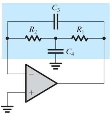
38 Realization of Transmission Zeros Values of s at which Z 2 (s) 0 and Z 1 (s) 0 Z 2 behaves as a short Values of s at which Z 1 (s) and Z 2 (s) Z 1 behaves as an open Realization of Filter Functions Low-Pass Filter High-Pass Filter Bandpass Filter T s V 1/LC V s + (1/RC)s + (1/LC) T s V s V s + (1/RC)s + (1/LC) T s V 1/RC s V s + (1/RC)s + (1/LC) 2-38
39 Notch Filter T s V s + (1/LC) V s + (1/RC)s + (1/LC) Low-Pass Notch Filter High-Pass Notch Filter T s V C s + (1/LC ) V C s + (1/RC)s + (1/LC) T s V s + (1/CL ) V s + (1/RC)s + (1/LC) ω 1/LC > ω 1/LC ω 1/CL < ω 1/LC 2-39
40 2.10 Second-Order Active Filters (Inductor Replacement) Second-Order Active Filters by Op Amp-RC Circuits Inductors are not suitable for IC implementation Use op amp-rc circuits to replace the inductors Second-order filter functions based on RLC resonator The Antoniou Inductance-Simulation Circuit Inductors are realized by op amp-rc circuits with negative feedbacks The equivalent inductance is given by Z V I sc / sl L C / 2-40
41 The Op Amp-RC Resonator The inductor is replaced by the Antoniou circuit The pole frequency and the quality factor are given by ω 1/ C L 1/ C C / Q ω C C /C A simplified case where R 1 R 2 R 3 R 5 R and C 4 C 6 C ω 1/RC Q /R 2-41
42 Filter Realization Low-Pass Filter High-Pass Filter Bandpass Filter Notch Filter 2-42
43 LPN Filter HPN Filter All-Pass Filter 2-43


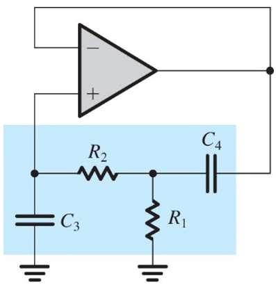
44 2.11 Second-Order Active Filters (Two-Integrator-Loop) Derivation of the Two-Integrator-Loop Biquad Integrator V i V o V i V o V 1 V src ω s High-pass implementation: V KV + 1 Q ω s V ω s V T s V V Ks s + ω /Q s + ω Band-pass implementation: T s ω s Kω s T s s + ω /Q s + ω Low-pass implementation: T s ω s Kω T s s + ω /Q s + ω 2-44
45 Circuit Implementation (I) - KHN Biquad V + V + V + V + V + ( ω /s)v + V + ( ω /s) V + T s V V + s + High-pass transfer function: s + + R ω s + + ω 1, Q , K 2 1 Q T s V V Ks s + (ω /Q)s + ω Band-pass transfer function: T s V V Kω s s + (ω /Q)s + ω Low-pass transfer function: T s V V Kω s + (ω /Q)s + ω Notch and all-pass transfer function: T s 1 V K R s ω R s + ω V s + (ω /Q)s + ω 2-45
s + ω Kω s + (ω /Q)s + ω An feedforward scheme can be employed T s V V C C s + 1 C 1 r s + 1 R C R s + (ω /Q)s + ω")
46 Circuit Implementation (II) Tow-Thomas Biquad Use an additional inverter to make all the coefficients of the summer the same sign All op amps are in single-ended mode The high-pass function is no longer available T s T s V V V V Kω s s + (ω /Q)s + ω Kω s + (ω /Q)s + ω An feedforward scheme can be employed T s V V C C s + 1 C 1 r s + 1 R C R s + (ω /Q)s + ω 2-46

 of the filter: V i V o A V A V 1 + Aβ The")
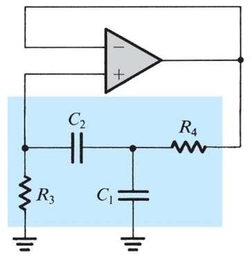
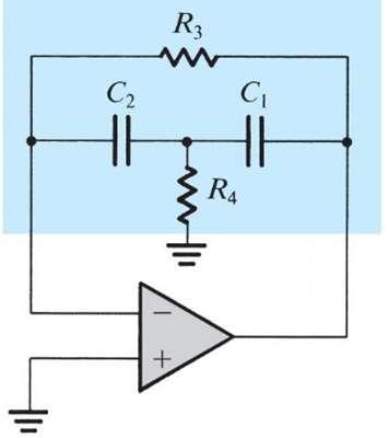
47 2.12 Single-Amplifier Biquadratic Active Filters Characteristics of the SAB Circuits Only one op amp is required to implement biquad circuit Exhibit a greater dependence on the limited gain and bandwidth of the op amp More sensitive to the unavoidable tolerances in the values of resistors and capacitors Limited to less stringent filter specifications with pole Q factors less than 10 Synthesis of the SAB Circuits The 2 nd -order filter is realized by a closed-loop system with an op amp and a RC feedback network Steps of SAB synthesis: Synthesis of a feedback loop with a pair of complex conjugate poles characterized by ω 0 and Q Injecting the input signal in a way that realizes the desired transmission zeros Natural modes (poles) of the filter: V i V o A V A V 1 + Aβ The closed-loop characteristic equation: 1 + Aβ At s 0 t s 1 A 0 The poles of the closed-loop system are identical to the zeros of the RC network 2-47

48 RC Networks with complex transmission zeros t s V V s + s s + s 1 C C R + C C C C C t s 1 C C V V s + s s + s 1 R C C C C 1 C C 1 C C Characteristics Equation of the Filter s + s ω ω Q + ω s + s 1 C C C C 1 C C Q C C 1 C + 1 C Let C 1 C 2 C, R 3 R, R 4 R/m m 4Q RC 2Q/ω 2-48
49 Injection the Input Signal The method of injection the input signal into the feedback loop through the grounded nodes A component with a ground node can be connected to the input source The filter transmission zeros depends on where the input signal is injected T s V V s α/c s + s 1 C + 1 C C C 2-49


50 Generation of Equivalent Feedback Loops Equivalent Loop Characteristics Equation: Characteristics Equation: β t(s) 1 + At s 0 t s 1 A 0 β 1 1 t s t(s) 1 + At s 0 t s 1 A

51 Generation of Equivalent Feedback Loops (Cont d) 2-51


52 Supplement Operational amplifier Circuit symbol for op amp Circuit model for ideal op amp
53 Supplement Negative feedback Opposite polarity to the change of output voltage due to negative feedback As output voltage v O increase v increases differential input (v + v ) decreases output v O decrease Finite output voltage with negative feedback For a finite input voltage v I, the output voltage v O is finite Assume v O v (R 2 v I + R 1 v O )/(R 1 + R 2 ) v + v < 0 v O Assume v O v (R 2 v I + R 1 v O )/(R 1 + R 2 ) v + v > 0 v O Using an ideal op amp in a negative feedback system Output voltage is finite The voltage gain of the op amp is infinite v + v v O /A 0 (virtual short)
54 Circuit analysis technique (1) Supplement Solve the nodal voltages and branch currents sequentially Basis of the circuit analysis: ohm s law, KVL and KCL v v / i v / v + i v + + v i v + v i v / 0 0 V i v / v v i + + v virtual short
55 Supplement Circuit analysis technique (2) Solve the circuit by nodal analysis Define the nodal voltages with necessary variables Specify branch currents based on the nodal voltages KCL for current equations Solve the simultaneous current equations i v / v i v v i v / 0 0 V i v / i + i 0 v + v 0 i + i + i 0 v + v + v v 0 v + + v
56 Supplement Weighted summer for coefficients with both signs v v v v v v v v v + v v v
57 Supplement Exercise 1: Assume the op amps are ideal, find the voltage gain (v o /v i ) of the following circuits. (1) (2) 4 V V V V 2 3 (3) (4) V V V V + V V V V Exercise 2: For a Miller integrator with R 10 k and C 10 nf, a shunt resistance R F is used to suppress the dc gain. Find the minimum value of R F if a period signal with a period of 0.1 s is applied at the input. ω > 10/(R F C) R F > 16 M
58 Supplement Exercise 3: Consider an inverting amplifier where the open-loop gain and 3-dB bandwidth of the op amp are and 10 rad/s, respectively. Find the gain and bandwidth of the close-loop gain (exact and approximated values) for the following cases: R 2 /R 1 1, 100, 200, and / G 1 + (1 + / )/A ω 1 + (1 + / )/A (1 + / )/ω A 1 / A G / ω ω A 1 + / ω G R 2 /R G o G 0 (approx.) ω 3dB ω 3dB (approx.)
59 Supplement Exercise 4: An op amp has an open-loop gain of 80 db and ω t of rad/s. (1) The op amp is used in an inverting amplifier with R 2 /R Find the close-loop gain at dc and at ω 1000 rad/s. (2) Two identical inverting amplifiers with R 2 /R are cascaded. Find the close-loop gain at dc and at ω 1000 rad/s. (3) For the cascaded amplifier in (2), find the frequency at which the gain is 3 db lower than the dc gain. (1) G(jω) -100/(1 + jω/1000); gain (@dc) -100; gain (@ω 1000) (2) G(jω) 10000/(1 + jω/1000) 2 ; gain (@dc) 10000; gain (@ω 1000) 5000 (3) G(jω) 10000/(1 + ω 2 / )7070 ω 643.8
60 Supplement Difference amplifier + i i i v v i v v + v i v v i v v v v i v / 1 + / v i i i i (v v )/ (v v )/ i i (v v )/ v / v v / 1 + / v v + v + v v v / v 1 + / + v / 1 + / + v / 1 + / v + v v + v + + v + v v / 1 + / v A / 1 + / + v A v + A v A 1 + / 1 + /

61 Supplement Instrumentation amplifier v v v R 2 v v v R 2 v v + v R 2 v + v v R 2
62 Supplement Difference amplifier with mismatch (1 + /2) (1 /2) A / / 2 ( + ) A 1 + / 1 + / ( + ) (1 /2) (1 + /2) For R 1 1 k, R k and 1% R 1 R 1 (1 + /2) R 3 R 1 (1 /2) R 2 R 2 (1 /2) R 4 R 2 (1 + /2) A R R A 100 A A CMRR A A 5100 (74dB) 1 v 1.1V, v 1V v 0.1V, v 1.05V v A v + A v V (desirable output 10V) 2 v 100.1V, v 100V v 0.1V, v V v A v + A v V (desirable output 10V)
 v v + v v 2 v v v v 2 v v v 1 + + v 2 v 1 + + 2 v v v + v 2 A 1 + + 2 v + v 2 1 + + 1 v 2 2 v v + 1 v 2 2 R 22 R 2 (1+/2) v 1 + v 5v v v + v 4 v + 0.01v v")
63 Supplement Instrumentation amplifier with mismatch Analysis of the first stage amplifier For R 1 20 k, R 2 80 k and 1% R 22 R 2 (1 + /2) R 21 R 2 (1 /2) R 21 R 2 (1-/2) v v + v v 2 v v v v 2 v v v v 2 v v v v + v 2 A v + v v 2 2 v v + 1 v 2 2 R 22 R 2 (1+/2) v 1 + v 5v v v + v 4 v v v
64 Supplement Instrumentation amplifier with mismatch Analysis of the complete instrumentation amplifier At the output of the first stage 1 + v + v A v + v v v v 1 + v v + v 2 v v v + v v A v + A v A A v + A v v A v + A v 1 + v + + v 2 v 1 + / 2 v 1 + / v + v 1 + / + v 1 + / 4 A 1 + A A 2 A A 1 + / CMRR A CMR
65 Supplement Instrumentation amplifier with mismatch For R 1 20 k, R 2 80 k, R 3 10 k, R k and 1% 1V 100V 0.802V V v A v + A v 99 k A A v + A v (1-/2) 79.2 k (1+/2) 1.01 k (1-/2) v + v 1 + / A A A (1+/2) 80.8 k (1-/2) 0.99 k (1+/2) A A / k V 1.1V 100.1V 1.302V V V v 0.1V 0.1V v 1 + / v 0.5V 0.5V v 1.05V V v v + v V V
66 Supplement Large-signal operation V O,max 15 V, I O,max 6 ma 1.5mA 1.5mA 15V Assuming voltage limited case: v O 15 V v I v O /A v 1.5 V i O 3 ma < 6 ma 1.5mA 10 k 1.5V 1mA 1mA 10V Assuming voltage limited case: v O 15 V v I v O /A v 1.5 V i O 9 ma > 6 ma (not allowed!) Reassuming current limited case: i F + i L v I /1 k + 10v I /2 k 6 ma v I 1 V and v O 10 V 1V 5mA 2 k
 ω p 1 k (rad/s) ω s 2 k (rad/s) A max 1 db A min 40 db Low-pass")
 0.707 (-3dB) A max Amin Spec B Spec A 0.316 (-10dB) 0.")
67 Supplement Filter specifications: Ideal low-pass filter ω p 1 k (rad/s) Low-pass filter (spec A) ω p 1 k (rad/s) ω s 2 k (rad/s) A max 1 db A min 40 db Low-pass filter (spec B) ω p 1 k (rad/s) ω s 3 k (rad/s) A max 3 db A min 10 db 1 (0dB) 0.89 (-1dB) (-3dB) A max Amin Spec B Spec A (-10dB) 0.01 (-40dB) 0 (-db) 0 ω p ω s ω s
68 Supplement Filter realization: (1) Filter spec (2) Transfer function (3) Ckt implementation Low-pass filter (spec B) ω p 1 k (rad/s) ω s 3 k (rad/s) A max 3 db A min 10 db 1 (0dB) 0.89 (-1dB) (-3dB) Multiple Choices T s s T jω jω(1 10 ) T ω 1k T ω 3k A max ( 3dB) ( 10dB) Multiple Choices Amin R 1 M, C 1 nf Spec B (-10dB) 0 (-db) 0 ω p ω s ω
69 Supplement Filter transfer functions: Examine the transfer functions T s s + 5s + 4s 10 s + 4s + 6s + 4 Filter implementations (s 1)(s j)(s + 3 j) (s + 2)(s j)(s + 1 j) T s s 6s + 10 s + 4s + 6s + 4 (s 3 + j)(s 3 j) (s + 2)(s j)(s + 1 j) T s T s s s + 4s + 6s s 2s (s 1 + j)(s 1 j) T s s + 5s + 4s 10 s + 4s + 6s + 4 (s 1)(s j)(s + 3 j) (s + 2)(s j)(s + 1 j) s 1 s + 2 s + 6s + 10 s + 2s + 2 The first term is a bilinear transfer function: 1 st order filter function The second term is a biquadratic transfer function: 2 nd order filter function Filters with high order transfer functions can be realized by cascading 1 st order and 2 nd order filters The circuits used to realize bilinear and biquadratic transfer functions will be introduced
70 Supplement First-order filters: T jω a jω + ω T jω a /ω a /ω 1 + jω/ω 1 + ω /ω T jω tan ω/ω T jω jωa a jω + ω 1 jω /ω T jω a 1 + ω /ω Example: 10 s T s s s + 10 T 1 R 1 R 2 10k T 2 C10nF T jω tan ω /ω R 1 R 2 10k C1nF 10 s + 10 T (s)t (s) s s + 10 T s 10 s /C s + 1/ C T s s s + 10 (/ )s s + 1/ C
71 Supplement First-order filters: (1) low-pass: a /ω > a ω pole < a /a (zero) (2) high-pass: a /ω < a ω pole > a /a (zero) 1/sC R + 1/sC V V + V 2 V V 1 src 1 + src s 1/RC s + 1/RC s ω s + ω
72 Second-order filters: T s T s General form for 2 nd -order filter: T s For two conjugate poles: Poles: s s + 3s + 2 s s s + 2s s j a s + a s + a s + b s + b a s + a s + a s + (ω /Q)s + ω (ω /Q) 4ω < 0 Q > 0.5 p, p ω 2Q ± jω 1 1 4Q 1 s + 2 Biquadratic transfer functions: T s T s T s Supplement (1st order filter) 2 1 s + 1 j a a s + b s + b s + (ω /Q)s + ω a s s + b s + b a s s + b s + b a s s + (ω /Q)s + ω a s s + (ω /Q)s + ω 2nd order filter T s a s + a a s + a s + b s + b s + (ω /Q)s + ω T s a s + a s s + b s + b a s + a s s + (ω /Q)s + ω T s a s + a a s + a s + b s + b s + (ω /Q)s + ω T s a s + a s + a s + b s + b a s + a s + a s + (ω /Q)s + ω
73 Low-pass filter: T s Supplement a a s + b s + b s + (ω /Q)s + ω Frequency response: T jω a ω + jω(ω /Q) + ω T jω a (ω ω ) +(ωω /Q) Monotonic decrease (Q < 0.707): T jω a ω ω + ωω Q a ω Q Gain peaking (Q > 0.707): ω T jω 0 ω ω 1 1 2Q and T jω a Q ω 1 1/(4Q )
74 High-pass filter: T s a s s + b s + b Supplement a s s + (ω /Q)s + ω Frequency response: a ω T jω ω + jω(ω /Q) + ω T jω a ω (ω ω ) +(ωω /Q) Monotonic decrease (Q < 0.707): T jω a ω a Q ω ω + ωω Q Gain peaking (Q > 0.707): ω T jω 0 ω ω / 1 1 2Q and T jω a Q 1 1/(4Q )
75 Supplement Band-pass filter: T s a s s + b s + b a s s + (ω /Q)s + ω Frequency response: Center frequency: ja ω T jω ω + jω(ω /Q) + ω T jω a Q ω T jω a ω (ω ω ) +(ωω /Q) 3-dB bandwidth: T jω a Q 2ω Q (ω ω ) +ω ω 2ω ω Q ω ω ±ω ω ω ω > ω Q ω ω ω ω ω ω 1 + 1/(4Q ) + ω /(2Q) ω ω < ω Q ω ω ω ω ω ω 1 + 1/(4Q ) ω /(2Q) BW ω ω ω /2Q
Homework Assignment 11
 Homework Assignment Question State and then explain in 2 3 sentences, the advantage of switched capacitor filters compared to continuous-time active filters. (3 points) Continuous time filters use resistors
Exercise s = 1. cos 60 ± j sin 60 = 0.5 ± j 3/2. = s 2 + s + 1. (s + 1)(s 2 + s + 1) T(jω) = (1 + ω2 )(1 ω 2 ) 2 + ω 2 (1 + ω 2 )
(s 2 + s + 1) T(jω) = (1 + ω2 )(1 ω 2 ) 2 + ω 2 (1 + ω 2 )") Exercise 7 Ex: 7. A 0 log T [db] T 0.99 0.9 0.8 0.7 0.5 0. 0 A 0 0. 3 6 0 Ex: 7. A max 0 log.05 0 log 0.95 0.9 db [ ] A min 0 log 40 db 0.0 Ex: 7.3 s + js j Ts k s + 3 + j s + 3 j s + 4 k s + s + 4 + 3
Exercise 7 Ex: 7. A 0 log T [db] T 0.99 0.9 0.8 0.7 0.5 0. 0 A 0 0. 3 6 0 Ex: 7. A max 0 log.05 0 log 0.95 0.9 db [ ] A min 0 log 40 db 0.0 Ex: 7.3 s + js j Ts k s + 3 + j s + 3 j s + 4 k s + s + 4 + 3
Filters and Tuned Amplifiers
 Filters and Tuned Amplifiers Essential building block in many systems, particularly in communication and instrumentation systems Typically implemented in one of three technologies: passive LC filters,
Sophomore Physics Laboratory (PH005/105)
") CALIFORNIA INSTITUTE OF TECHNOLOGY PHYSICS MATHEMATICS AND ASTRONOMY DIVISION Sophomore Physics Laboratory (PH5/15) Analog Electronics Active Filters Copyright c Virgínio de Oliveira Sannibale, 23 (Revision
CALIFORNIA INSTITUTE OF TECHNOLOGY PHYSICS MATHEMATICS AND ASTRONOMY DIVISION Sophomore Physics Laboratory (PH5/15) Analog Electronics Active Filters Copyright c Virgínio de Oliveira Sannibale, 23 (Revision
Electronic Circuits Summary
 Electronic Circuits Summary Andreas Biri, D-ITET 6.06.4 Constants (@300K) ε 0 = 8.854 0 F m m 0 = 9. 0 3 kg k =.38 0 3 J K = 8.67 0 5 ev/k kt q = 0.059 V, q kt = 38.6, kt = 5.9 mev V Small Signal Equivalent
Deliyannis, Theodore L. et al "Two Integrator Loop OTA-C Filters" Continuous-Time Active Filter Design Boca Raton: CRC Press LLC,1999
 Deliyannis, Theodore L. et al "Two Integrator Loop OTA-C Filters" Continuous-Time Active Filter Design Boca Raton: CRC Press LLC,1999 Chapter 9 Two Integrator Loop OTA-C Filters 9.1 Introduction As discussed
ECEN 325 Electronics
 ECEN 325 Electronics Introduction Dr. Aydın İlker Karşılayan Texas A&M University Department of Electrical and Computer Engineering Ohm s Law i R i R v 1 v v 2 v v 1 v 2 v = v 1 v 2 v = v 1 v 2 v = ir
Electronic Circuits EE359A
 Electronic Circuits EE359A Bruce McNair B26 bmcnair@stevens.edu 21-216-5549 Lecture 22 578 Second order LCR resonator-poles V o I 1 1 = = Y 1 1 + sc + sl R s = C 2 s 1 s + + CR LC s = C 2 sω 2 s + + ω
Operational amplifiers (Op amps)
") Operational amplifiers (Op amps) v R o R i v i Av i v View it as an ideal amp. Take the properties to the extreme: R i, R o 0, A.?!?!?!?! v v i Av i v A Consequences: No voltage dividers at input or output.
Operational amplifiers (Op amps) v R o R i v i Av i v View it as an ideal amp. Take the properties to the extreme: R i, R o 0, A.?!?!?!?! v v i Av i v A Consequences: No voltage dividers at input or output.
The general form for the transform function of a second order filter is that of a biquadratic (or biquad to the cool kids).
.") nd-order filters The general form for the transform function of a second order filter is that of a biquadratic (or biquad to the cool kids). T (s) A p s a s a 0 s b s b 0 As before, the poles of the transfer
nd-order filters The general form for the transform function of a second order filter is that of a biquadratic (or biquad to the cool kids). T (s) A p s a s a 0 s b s b 0 As before, the poles of the transfer
D is the voltage difference = (V + - V - ).
.") 1 Operational amplifier is one of the most common electronic building blocks used by engineers. It has two input terminals: V + and V -, and one output terminal Y. It provides a gain A, which is usually
1 Operational amplifier is one of the most common electronic building blocks used by engineers. It has two input terminals: V + and V -, and one output terminal Y. It provides a gain A, which is usually
Input and Output Impedances with Feedback
 EE 3 Lecture Basic Feedback Configurations Generalized Feedback Schemes Integrators Differentiators First-order active filters Second-order active filters Review from Last Time Input and Output Impedances
EE 508 Lecture 24. Sensitivity Functions - Predistortion and Calibration
 EE 508 Lecture 24 Sensitivity Functions - Predistortion and Calibration Review from last time Sensitivity Comparisons Consider 5 second-order lowpass filters (all can realize same T(s) within a gain factor)
ECEN 325 Electronics
 ECEN 325 Electronics Operational Amplifiers Dr. Aydın İlker Karşılayan Texas A&M University Department of Electrical and Computer Engineering Opamp Terminals positive supply inverting input terminal non
DESIGN MICROELECTRONICS ELCT 703 (W17) LECTURE 3: OP-AMP CMOS CIRCUIT. Dr. Eman Azab Assistant Professor Office: C
 LECTURE 3: OP-AMP CMOS CIRCUIT. Dr. Eman Azab Assistant Professor Office: C") MICROELECTRONICS ELCT 703 (W17) LECTURE 3: OP-AMP CMOS CIRCUIT DESIGN Dr. Eman Azab Assistant Professor Office: C3.315 E-mail: eman.azab@guc.edu.eg 1 TWO STAGE CMOS OP-AMP It consists of two stages: First
MICROELECTRONICS ELCT 703 (W17) LECTURE 3: OP-AMP CMOS CIRCUIT DESIGN Dr. Eman Azab Assistant Professor Office: C3.315 E-mail: eman.azab@guc.edu.eg 1 TWO STAGE CMOS OP-AMP It consists of two stages: First
EE 508 Lecture 4. Filter Concepts/Terminology Basic Properties of Electrical Circuits
 EE 58 Lecture 4 Filter Concepts/Terminology Basic Properties of Electrical Circuits Review from Last Time Filter Design Process Establish Specifications - possibly T D (s) or H D (z) - magnitude and phase
Speaker: Arthur Williams Chief Scientist Telebyte Inc. Thursday November 20 th 2008 INTRODUCTION TO ACTIVE AND PASSIVE ANALOG
 INTRODUCTION TO ACTIVE AND PASSIVE ANALOG FILTER DESIGN INCLUDING SOME INTERESTING AND UNIQUE CONFIGURATIONS Speaker: Arthur Williams Chief Scientist Telebyte Inc. Thursday November 20 th 2008 TOPICS Introduction
Frequency Dependent Aspects of Op-amps
 Frequency Dependent Aspects of Op-amps Frequency dependent feedback circuits The arguments that lead to expressions describing the circuit gain of inverting and non-inverting amplifier circuits with resistive
Lecture 6, ATIK. Switched-capacitor circuits 2 S/H, Some nonideal effects Continuous-time filters
 Lecture 6, ATIK Switched-capacitor circuits 2 S/H, Some nonideal effects Continuous-time filters What did we do last time? Switched capacitor circuits The basics Charge-redistribution analysis Nonidealties
ECE3050 Assignment 7
 ECE3050 Assignment 7. Sketch and label the Bode magnitude and phase plots for the transfer functions given. Use loglog scales for the magnitude plots and linear-log scales for the phase plots. On the magnitude
EE 230. Lecture 4. Background Materials
 EE 230 Lecture 4 Background Materials Transfer Functions Test Equipment in the Laboratory Quiz 3 If the input to a system is a sinusoid at KHz and if the output is given by the following expression, what
Analog Circuits and Systems
 Analog Circuits and Systems Prof. K Radhakrishna Rao Lecture 27: State Space Filters 1 Review Q enhancement of passive RC using negative and positive feedback Effect of finite GB of the active device on
Sinusoidal Steady-State Analysis
 Chapter 4 Sinusoidal Steady-State Analysis In this unit, we consider circuits in which the sources are sinusoidal in nature. The review section of this unit covers most of section 9.1 9.9 of the text.
Switched-Capacitor Circuits David Johns and Ken Martin University of Toronto
 Switched-Capacitor Circuits David Johns and Ken Martin University of Toronto (johns@eecg.toronto.edu) (martin@eecg.toronto.edu) University of Toronto 1 of 60 Basic Building Blocks Opamps Ideal opamps usually
ECEN 326 Electronic Circuits
 ECEN 326 Electronic Circuits Stability Dr. Aydın İlker Karşılayan Texas A&M University Department of Electrical and Computer Engineering Ideal Configuration V i Σ V ε a(s) V o V fb f a(s) = V o V ε (s)
Some of the different forms of a signal, obtained by transformations, are shown in the figure. jwt e z. jwt z e
 Transform methods Some of the different forms of a signal, obtained by transformations, are shown in the figure. X(s) X(t) L - L F - F jw s s jw X(jw) X*(t) F - F X*(jw) jwt e z jwt z e X(nT) Z - Z X(z)
CHAPTER 13 FILTERS AND TUNED AMPLIFIERS
 HAPTE FILTES AND TUNED AMPLIFIES hapter Outline. Filter Traniion, Type and Specification. The Filter Tranfer Function. Butterworth and hebyhev Filter. Firt Order and Second Order Filter Function.5 The
Texas A&M University Department of Electrical and Computer Engineering
 Texas A&M University Department of Electrical and Computer Engineering ECEN 622: Active Network Synthesis Homework #2, Fall 206 Carlos Pech Catzim 72300256 Page of .i) Obtain the transfer function of circuit
Schedule. ECEN 301 Discussion #20 Exam 2 Review 1. Lab Due date. Title Chapters HW Due date. Date Day Class No. 10 Nov Mon 20 Exam Review.
 Schedule Date Day lass No. 0 Nov Mon 0 Exam Review Nov Tue Title hapters HW Due date Nov Wed Boolean Algebra 3. 3.3 ab Due date AB 7 Exam EXAM 3 Nov Thu 4 Nov Fri Recitation 5 Nov Sat 6 Nov Sun 7 Nov Mon
Chapter 8: Converter Transfer Functions
 Chapter 8. Converter Transfer Functions 8.1. Review of Bode plots 8.1.1. Single pole response 8.1.2. Single zero response 8.1.3. Right half-plane zero 8.1.4. Frequency inversion 8.1.5. Combinations 8.1.6.
Prof. D. Manstretta LEZIONI DI FILTRI ANALOGICI. Danilo Manstretta AA
 AA-3 LEZIONI DI FILTI ANALOGICI Danilo Manstretta AA -3 AA-3 High Order OA-C Filters H() s a s... a s a s a n s b s b s b s b n n n n... The goal of this lecture is to learn how to design high order OA-C
Operational amplifiers (Op amps)
") Operational amplifiers (Op amps) Recall the basic two-port model for an amplifier. It has three components: input resistance, Ri, output resistance, Ro, and the voltage gain, A. v R o R i v d Av d v Also
Operational amplifiers (Op amps) Recall the basic two-port model for an amplifier. It has three components: input resistance, Ri, output resistance, Ro, and the voltage gain, A. v R o R i v d Av d v Also
Start with the transfer function for a second-order high-pass. s 2. ω o. Q P s + ω2 o. = G o V i
 aaac3xicbzfna9taeizxatkk7kec9tilqck4jbg5fjpca4ew0kmpdsrxwhlvxokl7titrirg69lr67s/robll64wmkna5jenndmvjstzyib9pfjntva/vzu6dzsnhj5/sdfefxhmvawzjpotsxeiliemxiucjpogkkybit3x5atow5w8xfugs5qmksecubqo7krlsfhkzsagxr4jne8wehaaxjqy4qq2svvl5el5qai2v9hy5tnxwb0om8igbiqfhhqhkoulcfs2zczhp26lwm7ph/hehffsbu90syo3hcmwvyxpawjtfbjpkm/wlbnximooweuygmsivnygqlpcmywvfppvrewjl3yqxti9gr6e2kgqbgrnlizqyuf2btqd/vgmo8cms4dllesrrdopz4ahyqjf7c66bovhzqznm9l89tqb2smixsxzk3tsdtnat4iaxnkk5bfcbn6iphqywpvxwtypgvnhtsvux234v77/ncudz9leyj84wplgvm7hrmk4ofi7ynw8edpwl7zt62o9klz8kl0idd8pqckq9krmaekz/kt7plbluf3a/un/d7ko6bc0zshbujz6huqq
Operational Amplifiers
 Operational Amplifiers A Linear IC circuit Operational Amplifier (op-amp) An op-amp is a high-gain amplifier that has high input impedance and low output impedance. An ideal op-amp has infinite gain and
University of Pennsylvania Department of Electrical and Systems Engineering ESE 319 Microelectronic Circuits. Final Exam 10Dec08 SOLUTIONS
 University of Pennsylvania Department of Electrical and Systems Engineering ESE 319 Microelectronic Circuits Final Exam 10Dec08 SOLUTIONS This exam is a closed book exam. Students are allowed to use a
Single-Time-Constant (STC) Circuits This lecture is given as a background that will be needed to determine the frequency response of the amplifiers.
 Circuits This lecture is given as a background that will be needed to determine the frequency response of the amplifiers.") Single-Time-Constant (STC) Circuits This lecture is given as a background that will be needed to determine the frequency response of the amplifiers. Objectives To analyze and understand STC circuits with
Single-Time-Constant (STC) Circuits This lecture is given as a background that will be needed to determine the frequency response of the amplifiers. Objectives To analyze and understand STC circuits with
Electronic Circuits EE359A
 Electronic Circuits EE359A Bruce McNair B26 bmcnair@stevens.edu 21-216-5549 Lecture 22 569 Second order section Ts () = s as + as+ a 2 2 1 ω + s+ ω Q 2 2 ω 1 p, p = ± 1 Q 4 Q 1 2 2 57 Second order section
EE221 Circuits II. Chapter 14 Frequency Response
 EE22 Circuits II Chapter 4 Frequency Response Frequency Response Chapter 4 4. Introduction 4.2 Transfer Function 4.3 Bode Plots 4.4 Series Resonance 4.5 Parallel Resonance 4.6 Passive Filters 4.7 Active
Chapter 33. Alternating Current Circuits
 Chapter 33 Alternating Current Circuits 1 Capacitor Resistor + Q = C V = I R R I + + Inductance d I Vab = L dt AC power source The AC power source provides an alternative voltage, Notation - Lower case
AC Circuits. The Capacitor
 The Capacitor Two conductors in close proximity (and electrically isolated from one another) form a capacitor. An electric field is produced by charge differences between the conductors. The capacitance
ENGN3227 Analogue Electronics. Problem Sets V1.0. Dr. Salman Durrani
 ENGN3227 Analogue Electronics Problem Sets V1.0 Dr. Salman Durrani November 2006 Copyright c 2006 by Salman Durrani. Problem Set List 1. Op-amp Circuits 2. Differential Amplifiers 3. Comparator Circuits
Chapter 10 Feedback. PART C: Stability and Compensation
 1 Chapter 10 Feedback PART C: Stability and Compensation Example: Non-inverting Amplifier We are analyzing the two circuits (nmos diff pair or pmos diff pair) to realize this symbol: either of the circuits
EE221 Circuits II. Chapter 14 Frequency Response
 EE22 Circuits II Chapter 4 Frequency Response Frequency Response Chapter 4 4. Introduction 4.2 Transfer Function 4.3 Bode Plots 4.4 Series Resonance 4.5 Parallel Resonance 4.6 Passive Filters 4.7 Active
Basics of Network Theory (Part-I)
") Basics of Network Theory (PartI). A square waveform as shown in figure is applied across mh ideal inductor. The current through the inductor is a. wave of peak amplitude. V 0 0.5 t (m sec) [Gate 987: Marks]
Basics of Network Theory (PartI). A square waveform as shown in figure is applied across mh ideal inductor. The current through the inductor is a. wave of peak amplitude. V 0 0.5 t (m sec) [Gate 987: Marks]
Lecture 4: Feedback and Op-Amps
 Lecture 4: Feedback and Op-Amps Last time, we discussed using transistors in small-signal amplifiers If we want a large signal, we d need to chain several of these small amplifiers together There s a problem,
Deliyannis, Theodore L. et al "Active Elements" Continuous-Time Active Filter Design Boca Raton: CRC Press LLC,1999
 Deliyannis, Theodore L. et al "Active Elements" Continuous-Time Active Filter Design Boca Raton: CRC Press LLC,999 Chapter 3 Active Elements 3. Introduction The ideal active elements are devices having
EE348L Lecture 1. EE348L Lecture 1. Complex Numbers, KCL, KVL, Impedance,Steady State Sinusoidal Analysis. Motivation
 EE348L Lecture 1 Complex Numbers, KCL, KVL, Impedance,Steady State Sinusoidal Analysis 1 EE348L Lecture 1 Motivation Example CMOS 10Gb/s amplifier Differential in,differential out, 5 stage dccoupled,broadband
Second-order filters. EE 230 second-order filters 1
 Second-order filters Second order filters: Have second order polynomials in the denominator of the transfer function, and can have zeroth-, first-, or second-order polynomials in the numerator. Use two
Master Degree in Electronic Engineering. Analog and Telecommunication Electronics course Prof. Del Corso Dante A.Y Switched Capacitor
 Master Degree in Electronic Engineering TOP-UIC Torino-Chicago Double Degree Project Analog and Telecommunication Electronics course Prof. Del Corso Dante A.Y. 2013-2014 Switched Capacitor Working Principles
CHAPTER 14 SIGNAL GENERATORS AND WAVEFORM SHAPING CIRCUITS
 CHAPTER 4 SIGNA GENERATORS AND WAEFORM SHAPING CIRCUITS Chapter Outline 4. Basic Principles of Sinusoidal Oscillators 4. Op Amp RC Oscillators 4.3 C and Crystal Oscillators 4.4 Bistable Multivibrators
First and Second Order Circuits. Claudio Talarico, Gonzaga University Spring 2015
 First and Second Order Circuits Claudio Talarico, Gonzaga University Spring 2015 Capacitors and Inductors intuition: bucket of charge q = Cv i = C dv dt Resist change of voltage DC open circuit Store voltage
EE-202 Exam III April 13, 2015
 EE-202 Exam III April 3, 205 Name: (Please print clearly.) Student ID: CIRCLE YOUR DIVISION DeCarlo-7:30-8:30 Furgason 3:30-4:30 DeCarlo-:30-2:30 202 2022 2023 INSTRUCTIONS There are 2 multiple choice
EE40 Midterm Review Prof. Nathan Cheung
 EE40 Midterm Review Prof. Nathan Cheung 10/29/2009 Slide 1 I feel I know the topics but I cannot solve the problems Now what? Slide 2 R L C Properties Slide 3 Ideal Voltage Source *Current depends d on
ELECTRONIC SYSTEMS. Basic operational amplifier circuits. Electronic Systems - C3 13/05/ DDC Storey 1
 Electronic Systems C3 3/05/2009 Politecnico di Torino ICT school Lesson C3 ELECTONIC SYSTEMS C OPEATIONAL AMPLIFIES C.3 Op Amp circuits» Application examples» Analysis of amplifier circuits» Single and
Name: (Please print clearly) Student ID: CIRCLE YOUR DIVISION INSTRUCTIONS
 Student ID: CIRCLE YOUR DIVISION INSTRUCTIONS") EE 202 Exam III April 13 2011 Name: (Please print clearly) Student ID: CIRCLE YOUR DIVISION Morning 7:30 MWF Furgason INSTRUCTIONS Afternoon 3:30 MWF DeCarlo There are 10 multiple choice worth 5 points
EE 202 Exam III April 13 2011 Name: (Please print clearly) Student ID: CIRCLE YOUR DIVISION Morning 7:30 MWF Furgason INSTRUCTIONS Afternoon 3:30 MWF DeCarlo There are 10 multiple choice worth 5 points
ECE 255, Frequency Response
 ECE 255, Frequency Response 19 April 2018 1 Introduction In this lecture, we address the frequency response of amplifiers. This was touched upon briefly in our previous lecture in Section 7.5 of the textbook.
ECEN 607 (ESS) Op-Amps Stability and Frequency Compensation Techniques. Analog & Mixed-Signal Center Texas A&M University
 Op-Amps Stability and Frequency Compensation Techniques. Analog & Mixed-Signal Center Texas A&M University") ECEN 67 (ESS) Op-Amps Stability and Frequency Compensation Techniques Analog & Mixed-Signal Center Texas A&M University Stability of Linear Systems Harold S. Black, 97 Negative feedback concept Negative
ECEN 67 (ESS) Op-Amps Stability and Frequency Compensation Techniques Analog & Mixed-Signal Center Texas A&M University Stability of Linear Systems Harold S. Black, 97 Negative feedback concept Negative
Biquad Filter. by Kenneth A. Kuhn March 8, 2013
 by Kenneth A. Kuhn March 8, 201 The biquad filter implements both a numerator and denominator quadratic function in s thus its name. All filter outputs have identical second order denominator in s and
Sinusoidal Steady State Analysis (AC Analysis) Part I
 Part I") Sinusoidal Steady State Analysis (AC Analysis) Part I Amin Electronics and Electrical Communications Engineering Department (EECE) Cairo University elc.n102.eng@gmail.com http://scholar.cu.edu.eg/refky/
Sinusoidal Steady State Analysis (AC Analysis) Part I Amin Electronics and Electrical Communications Engineering Department (EECE) Cairo University elc.n102.eng@gmail.com http://scholar.cu.edu.eg/refky/
Notes for course EE1.1 Circuit Analysis TOPIC 10 2-PORT CIRCUITS
 Objectives: Introduction Notes for course EE1.1 Circuit Analysis 4-5 Re-examination of 1-port sub-circuits Admittance parameters for -port circuits TOPIC 1 -PORT CIRCUITS Gain and port impedance from -port
Electronics. Basics & Applications. group talk Daniel Biesinger
 Electronics Basics & Applications group talk 23.7.2010 by Daniel Biesinger 1 2 Contents Contents Basics Simple applications Equivalent circuit Impedance & Reactance More advanced applications - RC circuits
Prof. Anyes Taffard. Physics 120/220. Voltage Divider Capacitor RC circuits
 Prof. Anyes Taffard Physics 120/220 Voltage Divider Capacitor RC circuits Voltage Divider The figure is called a voltage divider. It s one of the most useful and important circuit elements we will encounter.
Op-Amp Circuits: Part 3
 Op-Amp Circuits: Part 3 M. B. Patil mbpatil@ee.iitb.ac.in www.ee.iitb.ac.in/~sequel Department of Electrical Engineering Indian Institute of Technology Bombay Introduction to filters Consider v(t) = v
Laplace Transform Analysis of Signals and Systems
 Laplace Transform Analysis of Signals and Systems Transfer Functions Transfer functions of CT systems can be found from analysis of Differential Equations Block Diagrams Circuit Diagrams 5/10/04 M. J.
Time Varying Circuit Analysis
 MAS.836 Sensor Systems for Interactive Environments th Distributed: Tuesday February 16, 2010 Due: Tuesday February 23, 2010 Problem Set # 2 Time Varying Circuit Analysis The purpose of this problem set
QUESTION BANK SUBJECT: NETWORK ANALYSIS (10ES34)
") QUESTION BANK SUBJECT: NETWORK ANALYSIS (10ES34) NOTE: FOR NUMERICAL PROBLEMS FOR ALL UNITS EXCEPT UNIT 5 REFER THE E-BOOK ENGINEERING CIRCUIT ANALYSIS, 7 th EDITION HAYT AND KIMMERLY. PAGE NUMBERS OF
QUESTION BANK SUBJECT: NETWORK ANALYSIS (10ES34) NOTE: FOR NUMERICAL PROBLEMS FOR ALL UNITS EXCEPT UNIT 5 REFER THE E-BOOK ENGINEERING CIRCUIT ANALYSIS, 7 th EDITION HAYT AND KIMMERLY. PAGE NUMBERS OF
Response of Second-Order Systems
 Unit 3 Response of SecondOrder Systems In this unit, we consider the natural and step responses of simple series and parallel circuits containing inductors, capacitors and resistors. The equations which
Chapter 2. Engr228 Circuit Analysis. Dr Curtis Nelson
 Chapter 2 Engr228 Circuit Analysis Dr Curtis Nelson Chapter 2 Objectives Understand symbols and behavior of the following circuit elements: Independent voltage and current sources; Dependent voltage and
2nd-order filters. EE 230 second-order filters 1
 nd-order filters Second order filters: Have second order polynomials in the denominator of the transfer function, and can have zeroth-, first-, or second-order polyinomials in the numerator. Use two reactive
Studio 9 Review Operational Amplifier Stability Compensation Miller Effect Phase Margin Unity Gain Frequency Slew Rate Limiting Reading: Text sec 5.
 Studio 9 Review Operational Amplifier Stability Compensation Miller Effect Phase Margin Unity Gain Frequency Slew Rate Limiting Reading: Text sec 5.2 pp. 232-242 Two-stage op-amp Analysis Strategy Recognize
Bandwidth of op amps. R 1 R 2 1 k! 250 k!
 Bandwidth of op amps An experiment - connect a simple non-inverting op amp and measure the frequency response. From the ideal op amp model, we expect the amp to work at any frequency. Is that what happens?
4/27 Friday. I have all the old homework if you need to collect them.
 4/27 Friday Last HW: do not need to turn it. Solution will be posted on the web. I have all the old homework if you need to collect them. Final exam: 7-9pm, Monday, 4/30 at Lambert Fieldhouse F101 Calculator
Case Study: Parallel Coupled- Line Combline Filter
 MICROWAVE AND RF DESIGN MICROWAVE AND RF DESIGN Case Study: Parallel Coupled- Line Combline Filter Presented by Michael Steer Reading: 6. 6.4 Index: CS_PCL_Filter Based on material in Microwave and RF
Electronic Circuits. Prof. Dr. Qiuting Huang Integrated Systems Laboratory
 Electronic Circuits Prof. Dr. Qiuting Huang 6. Transimpedance Amplifiers, Voltage Regulators, Logarithmic Amplifiers, Anti-Logarithmic Amplifiers Transimpedance Amplifiers Sensing an input current ii in
Sinusoidal Steady State Analysis (AC Analysis) Part II
 Part II") Sinusoidal Steady State Analysis (AC Analysis) Part II Amin Electronics and Electrical Communications Engineering Department (EECE) Cairo University elc.n102.eng@gmail.com http://scholar.cu.edu.eg/refky/
Sinusoidal Steady State Analysis (AC Analysis) Part II Amin Electronics and Electrical Communications Engineering Department (EECE) Cairo University elc.n102.eng@gmail.com http://scholar.cu.edu.eg/refky/
Chapter 10 AC Analysis Using Phasors
 Chapter 10 AC Analysis Using Phasors 10.1 Introduction We would like to use our linear circuit theorems (Nodal analysis, Mesh analysis, Thevenin and Norton equivalent circuits, Superposition, etc.) to
ECE 202 Fall 2013 Final Exam
 ECE 202 Fall 2013 Final Exam December 12, 2013 Circle your division: Division 0101: Furgason (8:30 am) Division 0201: Bermel (9:30 am) Name (Last, First) Purdue ID # There are 18 multiple choice problems
Ver 3537 E1.1 Analysis of Circuits (2014) E1.1 Circuit Analysis. Problem Sheet 1 (Lectures 1 & 2)
 E1.1 Circuit Analysis. Problem Sheet 1 (Lectures 1 & 2)") Ver 3537 E. Analysis of Circuits () Key: [A]= easy... [E]=hard E. Circuit Analysis Problem Sheet (Lectures & ). [A] One of the following circuits is a series circuit and the other is a parallel circuit.
Ver 3537 E. Analysis of Circuits () Key: [A]= easy... [E]=hard E. Circuit Analysis Problem Sheet (Lectures & ). [A] One of the following circuits is a series circuit and the other is a parallel circuit.
Sinusoids and Phasors
 CHAPTER 9 Sinusoids and Phasors We now begins the analysis of circuits in which the voltage or current sources are time-varying. In this chapter, we are particularly interested in sinusoidally time-varying
Circuit Analysis-III. Circuit Analysis-II Lecture # 3 Friday 06 th April, 18
 Circuit Analysis-III Sinusoids Example #1 ü Find the amplitude, phase, period and frequency of the sinusoid: v (t ) =12cos(50t +10 ) Signal Conversion ü From sine to cosine and vice versa. ü sin (A ± B)
UNIVERSITY OF CALIFORNIA College of Engineering Department of Electrical Engineering and Computer Sciences
 UNIVERSITY OF CALIFORNIA College of Engineering Department of Electrical Engineering and Computer Sciences E. Alon Final EECS 240 Monday, May 19, 2008 SPRING 2008 You should write your results on the exam
Lecture 9 Time Domain vs. Frequency Domain
 . Topics covered Lecture 9 Time Domain vs. Frequency Domain (a) AC power in the time domain (b) AC power in the frequency domain (c) Reactive power (d) Maximum power transfer in AC circuits (e) Frequency
EE313 Fall 2013 Exam #1 (100 pts) Thursday, September 26, 2013 Name. 1) [6 pts] Convert the following time-domain circuit to the RMS Phasor Domain.
![EE313 Fall 2013 Exam #1 (100 pts) Thursday, September 26, 2013 Name. 1) [6 pts] Convert the following time-domain circuit to the RMS Phasor Domain.](/thumbs/95/123488230.jpg "EE313 Fall 2013 Exam #1 (100 pts) Thursday, September 26, 2013 Name. 1) [6 pts] Convert the following time-domain circuit to the RMS Phasor Domain.") Name If you have any questions ask them. Remember to include all units on your answers (V, A, etc). Clearly indicate your answers. All angles must be in the range 0 to +180 or 0 to 180 degrees. 1) [6 pts]
Name If you have any questions ask them. Remember to include all units on your answers (V, A, etc). Clearly indicate your answers. All angles must be in the range 0 to +180 or 0 to 180 degrees. 1) [6 pts]
University of Illinois at Chicago Spring ECE 412 Introduction to Filter Synthesis Homework #4 Solutions
 Problem 1 A Butterworth lowpass filter is to be designed having the loss specifications given below. The limits of the the design specifications are shown in the brick-wall characteristic shown in Figure
Midterm Exam (closed book/notes) Tuesday, February 23, 2010
 Tuesday, February 23, 2010") University of California, Berkeley Spring 2010 EE 42/100 Prof. A. Niknejad Midterm Exam (closed book/notes) Tuesday, February 23, 2010 Guidelines: Closed book. You may use a calculator. Do not unstaple
University of California, Berkeley Spring 2010 EE 42/100 Prof. A. Niknejad Midterm Exam (closed book/notes) Tuesday, February 23, 2010 Guidelines: Closed book. You may use a calculator. Do not unstaple
EE100Su08 Lecture #9 (July 16 th 2008)
") EE100Su08 Lecture #9 (July 16 th 2008) Outline HW #1s and Midterm #1 returned today Midterm #1 notes HW #1 and Midterm #1 regrade deadline: Wednesday, July 23 rd 2008, 5:00 pm PST. Procedure: HW #1: Bart
EE100Su08 Lecture #9 (July 16 th 2008) Outline HW #1s and Midterm #1 returned today Midterm #1 notes HW #1 and Midterm #1 regrade deadline: Wednesday, July 23 rd 2008, 5:00 pm PST. Procedure: HW #1: Bart
Lecture 7, ATIK. Continuous-time filters 2 Discrete-time filters
 Lecture 7, ATIK Continuous-time filters 2 Discrete-time filters What did we do last time? Switched capacitor circuits with nonideal effects in mind What should we look out for? What is the impact on system
Refinements to Incremental Transistor Model
 Refinements to Incremental Transistor Model This section presents modifications to the incremental models that account for non-ideal transistor behavior Incremental output port resistance Incremental changes
Sample-and-Holds David Johns and Ken Martin University of Toronto
 Sample-and-Holds David Johns and Ken Martin (johns@eecg.toronto.edu) (martin@eecg.toronto.edu) slide 1 of 18 Sample-and-Hold Circuits Also called track-and-hold circuits Often needed in A/D converters
EE-202 Exam III April 6, 2017
 EE-202 Exam III April 6, 207 Name: (Please print clearly.) Student ID: CIRCLE YOUR DIVISION DeCarlo--202 DeCarlo--2022 7:30 MWF :30 T-TH INSTRUCTIONS There are 3 multiple choice worth 5 points each and
Poles, Zeros, and Frequency Response
 Complex Poles Poles, Zeros, and Frequency esponse With only resistors and capacitors, you're stuck with real poles. If you want complex poles, you need either an op-amp or an inductor as well. Complex
ECE Networks & Systems
 ECE 342 1. Networks & Systems Jose E. Schutt Aine Electrical & Computer Engineering University of Illinois jschutt@emlab.uiuc.edu 1 What is Capacitance? 1 2 3 Voltage=0 No Charge No Current Voltage build
Figure Circuit for Question 1. Figure Circuit for Question 2
 Exercises 10.7 Exercises Multiple Choice 1. For the circuit of Figure 10.44 the time constant is A. 0.5 ms 71.43 µs 2, 000 s D. 0.2 ms 4 Ω 2 Ω 12 Ω 1 mh 12u 0 () t V Figure 10.44. Circuit for Question
FEEDBACK AND STABILITY
 FEEDBCK ND STBILITY THE NEGTIVE-FEEDBCK LOOP x IN X OUT x S + x IN x OUT Σ Signal source _ β Open loop Closed loop x F Feedback network Output x S input signal x OUT x IN x F feedback signal x IN x S x
Chapter 10: Sinusoids and Phasors
 Chapter 10: Sinusoids and Phasors 1. Motivation 2. Sinusoid Features 3. Phasors 4. Phasor Relationships for Circuit Elements 5. Impedance and Admittance 6. Kirchhoff s Laws in the Frequency Domain 7. Impedance
6.1 Introduction
 6. Introduction A.C Circuits made up of resistors, inductors and capacitors are said to be resonant circuits when the current drawn from the supply is in phase with the impressed sinusoidal voltage. Then.
Radivoje Đurić, 2015, Analogna Integrisana Kola 1
 OVA & OTA 1 OVA VA-Operational Voltage Amplifier Ideally a voltage-controlled voltage source Typically contains an output stage that can drive arbitrary loads, including small resistances Predominantly
Designing Information Devices and Systems I Fall 2018 Lecture Notes Note Introduction: Op-amps in Negative Feedback
 EECS 16A Designing Information Devices and Systems I Fall 2018 Lecture Notes Note 18 18.1 Introduction: Op-amps in Negative Feedback In the last note, we saw that can use an op-amp as a comparator. However,
Resonant Matching Networks
 Chapter 1 Resonant Matching Networks 1.1 Introduction Frequently power from a linear source has to be transferred into a load. If the load impedance may be adjusted, the maximum power theorem states that
Lecture 37: Frequency response. Context
 EECS 05 Spring 004, Lecture 37 Lecture 37: Frequency response Prof J. S. Smith EECS 05 Spring 004, Lecture 37 Context We will figure out more of the design parameters for the amplifier we looked at in