Written exam for IE1204/5 Digital Design with solutions Thursday 29/
|
|
|
- Nora Holland
- 5 years ago
- Views:
Transcription

1 Written exam for IE4/5 Digital Design with solutions Thursday 9/ General Information Examiner: Ingo Sander. Teacher: William Sandqvist phone Exam text does not have to be returned when you hand in your writing. Aids: No aids are allowed! The exam consists of three parts with a total of 4 tasks, and a total of points: Part A (Analysis) containes ten short questions. Right answer will give you one point. Incorrect answer will give you zero points. The total number of points in Part A is points. To pass the Part A requires at least 6p, if fewer points we will not look at the rest of your exam. Part A (Methods) contains two method problems on a total of points. To pass the exam requires at least points from A + A, if fewer points we will not look at the rest of your exam. Part B (Design problems) contains two design problems of a total of points. Part B is corrected only if there are at least p from the exam A- Part. NOTE! At the end of the exam text there is a submission sheet for Part A, which shall be separated to be submitted together with the solutions for A and B. For a passing grade (E ) requires at least points on the exam. If exactly p from A(6p)+A(4p), (FX), completion to (E) will be offered. Grades are given as follows: F E D C B A The result is expected to be announced before Thursday 9/ 5.
2 Part A: Analysis Only answers are needed in Part A. Write the answers on the submission sheet for Part A, which can be found at the end of the exam text.. p/p A function f(x, y, z) is described by the expression: f ( x, y, z) x y z x y z ( y z) Write down the function maxterms, eg. the function as a product of sums. f ( x, y, z) PoS?. Proposed solution f ( x, y, z) x y z x y z ( y z) ( x y z) xyz yz x y z x z y( z) ( x y z) only one maxterm is needed. p/p A four bit unsigned integer x (xxxx) is to be multiplicated by the constant 7. This is done by connecting the number x to a seven bit adder that is configured to do the operation y = 7x = (8x x) Draw how the adder is to be configured. Except the four bits in x there are also bits with the values and if needed. You will find a copy of the figure on the submission sheet. yz( x ). Proposed solution y 7 x (8 x x). p/p Two binary 6 bit two complement numbers are added. What will the result be expressed as a signed decimal number?. Proposed solution + = = = -7
 as much as possible. 5. Proposed solution Y A A B B A A B B A A B B 6.")
 { SoP} bc abc bc bc abc bc abc ( a a) bc abc abc abc f ( c, b, a) { PoS} min ( b c)( b c)( a c) or ( b c)( b c)( a b)")
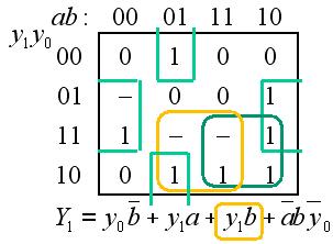
3 4. p/p Given is a Karnaugh map for a function of four variables y = f(x, x, x, x). Write the function as a minimized ymin sum of products, SoP form. - in the map means don t care. 4. Proposed solution y x x x x xxx 5. p/p The figure bellow shows a circuit with two NAND gates and one NOR-gate. Simplify the function Y = f(a, B) as much as possible. 5. Proposed solution Y A A B B A A B B A A B B 6. p/p A logic function of three variables c b a is realized with multiplexors. Write the function on minimized PoS form (as a product of sums). f ( c, b, a) { PoS} min? 6. Proposed solution f ( c, b, a) { SoP} bc abc bc bc abc bc abc ( a a) bc abc abc abc f ( c, b, a) { PoS} min ( b c)( b c)( a c) or ( b c)( b c)( a b)

4 7. p/p Give an expression for the logical function realized by the CMOS circuit in the figure? Y = f(a,b,c) =? 7. Proposed solution PDN : Y acbc Y Y acbc CMOS Multiplexor 8. p/p Complete the timing diagram for the D-latch and D-flipflop by drawing signal Q for booth cases. Draw the figure so that it is clear what is causing the changes in the Q! 8. Proposed solution 4

5 9. p/p The figure shows a synchronous decade counter (QDQCQBQA 9). Mark (= draw in the figure on the answer sheet) the critical path that determines how fast the counter can count. Calculate the minimum time T [ns] between the clock pulses that still provides safe operation. Gates: tpdor = 4, tpdand = 5 [ns] 9. proposed solution Flip-flops: tsu =, th =, tpdq = [ns] T t pdq t psand t psand ns t psor t su. p/p Below is the VHDL code for a : multiplexer. The multiplexer Karnaugh map is shown at right. Complete code so that it becomes a Hazard free MUX. The line of code is also available on the answer sheet. -- import std_logic from the IEEE library library IEEE; use IEEE.std_logic_64.all; -- this is the entity entity MUX is port ( a : in std_logic; b : in std_logic; c : in std_logic; Y : out std_logic); end entity MUX; -- this is the architecture architecture gates of MUX is begin Y <= (b AND c) OR (a AND NOT c) end architecture gates;. Proposed solution Y <= (b AND c) OR (a AND NOT c) OR (a AND b); 5
6 Part A: Methods Note! Part A will only be corrected if you have passed part A ( 6p). 5p One older instrument has a seven segment display with seven light bulbs, but it lacks an outlet for connection to a computer. One could therefore need a combinatorial circuit that connects to the bulbs and then converts 7-segment code to the usual BCD code (normal binary coded digits to 9) that is used by a variety of other equipments. a) (p) Set up the truth table for the ten BCD numbers. Black segment is in figure. ( x ) xxx BCD f ( abcdefg) b) (p) Inspect the truth table. You can discover that even if up to two of the segments are excluded as inputs, the relationship remains distinct between image segments and BCD digits. Find one/two segments that you can do without? Derive the new truth-table without this/these segments. c) (p) Draw the karnaugh maps for the four BCD-code bits and derive the minimized expressions for x x x x in SoP-form. Segment combinations that never occurs should be exploited as don t care. (With the excluded segments in the truth table, the number of variables will be manageable). d) (p) Choose yourself one of the expressions x x x x and realize it using only input NAND gates. (No inverted variables are available). Proposed solution abcdefg x xxx Segment a is necessary distinguish between and 7. Segment e is needed to distinguish between 8 from 9 and 5 from 6. Segments c and d could be excluded without the encoding becoming ambiguous. See the figure. This can be used to simplify the problem down to 5 variables abefg x xxx 6
 (p) Analyze the sequential circuits in the figure and draw the full state diagram and the full state table.")
7 x abfg x b a f g af x a f be x f g ae Example. Bit x :. 5p The figure shows a "self-correcting ring counter" counting the "one hot" sequence qqqq,,,. a) (p) Analyze the sequential circuits in the figure and draw the full state diagram and the full state table. If the counter would start in any other state than any of the four desired "one hot" states, how many clock pulses are required, in the worst case, before the counter has "corrected" this and ends up in the correct sequence? 7
8 b) (p) You can also get the same "one-hot" sequence from a Moore machine with four states, see the state diagram to the right. Derive this sequential circuit with D-flip-flops and optional gates. Use the state encoding from the state diagram. Draw the schematic of the circuit.. Proposed solution q q q q q q q q Q Q q q q q Q Q q q q q q Inspection of table gives: Q Q Q Q Decoding: A Q Q C Q Q q q q qqqd d q q q After at most three clock pulses the one hot sequency will be reached! B Q Q D Q Q 8
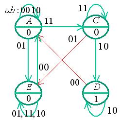
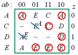
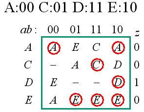
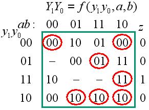
9 Part B. Design Problems Note! Part B will only be corrected if you have passed part A+A ( p).. 4p Sequence Detector. Different inputs three in a row. You will design a synchronous sequential circuit, in the form of a positive edge-triggered Moore machine with D flip-flops. The input signals a and b are synchronized with the clock pulses C. The output signal z will be when a and b are different in at least three consecutive clock pulse intervals. For other sequences z must be equal to. a) (p) Derive the circuit state table and draw the state diagram. b) (p) Use the Gray code to encode the states and derive the encoded state table. Derive the minimized expressions for next state and for the output. c) (p) Draw the next state decoder circuit, there is only access to AND, OR, and XOR gates.. Proposed solution z q q 4. 6p Inside pulse detector. An asynchronous sequential circuit "Compares" pulses received on two inputs a and b. The pulse at the b input is always a little shorter than the pulse of a, and there will be at most one b-pulse during the interval a. b-pulses will arrive randomly relative to the a-pulse. (There are no exact simultaneous events). 9

 Simplify the state diagram by combining compatible state. (Hint.")
.")
10 Sequence circuit must indicate the case when b is started (becomes one) after a has started (become one), and b has finished (become ) before a finish (become ). The output z will then be = from b's trailing edge to a's trailing edge. z must be for all other cases. See the figure time diagram illustrating this case. a) First, set up a proper flow table for the sequence circuit. You don t need from the beginning to care about minimizing the number of states. All positions in the table that can not occur should be treated as don t care. b) Simplify the state diagram by combining compatible state. (Hint. Various solutions are possible, there is among them a solution with four states). c) Do a suitable state assignement with an exitation table which gives a circuit that is free of critical race. (Hint. Various solutions are possible, there is a solution with two state variables exploiting unstable transition states and uncritical race). You should also derive hazard free expressions for the next state and an expression for output, and draw the circuits with the use of optional gates.. Proposed solution derive state chart step by step - can not occur, double change in input * has not occurred in any of the possible sequences, then will not occur
11 Remove intersecting lines by inserting transition states to avoid hamming distance. z y y y b Hazard cover Good Luck!
12 Submission sheet for Part A Sheet (remove and hand in together with your answers for part A and part B ) Last name: Given name: Personal code: Sheet: Write down your answers for the questions from Part A ( to ) Question Answer f ( x, y, z) PoS? y = 7x = (8x x) Signed decimal?? = f 5 Y f ( A, B)? 4 x, x, x, x ) SoP? ( min 6 f ( c, b, a) { PoS} min? 7 Y = f(a,b,c) =? 8 9 T [ns] = Y <= (b AND c) OR (a AND NOT c) This table is completed by the examiner!! Part A () Part A () Part B () Total () Poäng 4 Sum Grade
Written reexam with solutions for IE1204/5 Digital Design Monday 14/
 Written reexam with solutions for IE204/5 Digital Design Monday 4/3 206 4.-8. General Information Examiner: Ingo Sander. Teacher: William Sandqvist phone 08-7904487 Exam text does not have to be returned
Written exam with solutions IE Digital Design Friday 21/
 Written exam with solutions IE204-5 Digital Design Friday 2/0 206 09.00-3.00 General Information Examiner: Ingo Sander. Teacher: Kista, William Sandvist tel 08-7904487, Elena Dubrova phone 08-790 4 4 Exam
Written exam with solutions IE1204/5 Digital Design Friday 13/
 Written eam with solutions IE204/5 Digital Design Friday / 207 08.00-2.00 General Information Eaminer: Ingo Sander. Teacher: Kista, William Sandqvist tel 08-7904487 Teacher: Valhallavägen, Ahmed Hemani
Written exam with solutions IE1204/5 Digital Design Monday 23/
 Written exam with solutions IE204/5 Digital Design Monday 23/0 207 4.00-8.00 General Information Examiner: Ingo Sander. Teacher: Kista, William Sandvist Exam text has to be returned when you hand in your
Philadelphia University Student Name: Student Number:
 Philadelphia University Student Name: Student Number: Faculty of Engineering Serial Number: Final Exam, First Semester: 2017/2018 Dept. of Computer Engineering Course Title: Logic Circuits Date: 29/01/2018
Dr. Nicola Nicolici COE/EE2DI4 Midterm Test #2 Nov 22, 2006
 COE/EE2DI4 Midterm Test #2 Fall 2006 Page 1 Dr. Nicola Nicolici COE/EE2DI4 Midterm Test #2 Nov 22, 2006 Instructions: This examination paper includes 12 pages and 20 multiple-choice questions starting
EE40 Lec 15. Logic Synthesis and Sequential Logic Circuits
 EE40 Lec 15 Logic Synthesis and Sequential Logic Circuits Prof. Nathan Cheung 10/20/2009 Reading: Hambley Chapters 7.4-7.6 Karnaugh Maps: Read following before reading textbook http://www.facstaff.bucknell.edu/mastascu/elessonshtml/logic/logic3.html
Reg. No. Question Paper Code : B.E./B.Tech. DEGREE EXAMINATION, NOVEMBER/DECEMBER Second Semester. Computer Science and Engineering
 Sp 6 Reg. No. Question Paper Code : 27156 B.E./B.Tech. DEGREE EXAMINATION, NOVEMBER/DECEMBER 2015. Second Semester Computer Science and Engineering CS 6201 DIGITAL PRINCIPLES AND SYSTEM DESIGN (Common
 vidyarthiplus.com vidyarthiplus.com vidyarthiplus.com ANNA UNIVERSITY- COMBATORE B.E./ B.TECH. DEGREE EXAMINATION - JUNE 2009. ELECTRICAL & ELECTONICS ENGG. - FOURTH SEMESTER DIGITAL LOGIC CIRCUITS PART-A
Philadelphia University Student Name: Student Number:
 Philadelphia University Student Name: Student Number: Faculty of Engineering Serial Number: Final Exam, Second Semester: 2015/2016 Dept. of Computer Engineering Course Title: Logic Circuits Date: 08/06/2016
Sample Test Paper - I
 Scheme G Sample Test Paper - I Course Name : Computer Engineering Group Marks : 25 Hours: 1 Hrs. Q.1) Attempt any THREE: 09 Marks a) Define i) Propagation delay ii) Fan-in iii) Fan-out b) Convert the following:
The Design Procedure. Output Equation Determination - Derive output equations from the state table
 The Design Procedure Specification Formulation - Obtain a state diagram or state table State Assignment - Assign binary codes to the states Flip-Flop Input Equation Determination - Select flipflop types
KUMARAGURU COLLEGE OF TECHNOLOGY COIMBATORE
 Estd-1984 KUMARAGURU COLLEGE OF TECHNOLOGY COIMBATORE 641 006 QUESTION BANK UNIT I PART A ISO 9001:2000 Certified 1. Convert (100001110.010) 2 to a decimal number. 2. Find the canonical SOP for the function
ELECTRONICS & COMMUNICATION ENGINEERING PROFESSIONAL ETHICS AND HUMAN VALUES
 EC 216(R-15) Total No. of Questions :09] [Total No. of Pages : 02 II/IV B.Tech. DEGREE EXAMINATIONS, DECEMBER- 2016 First Semester ELECTRONICS & COMMUNICATION ENGINEERING PROFESSIONAL ETHICS AND HUMAN
Fundamentals of Digital Design
 Fundamentals of Digital Design Digital Radiation Measurement and Spectroscopy NE/RHP 537 1 Binary Number System The binary numeral system, or base-2 number system, is a numeral system that represents numeric
Department of Electrical & Electronics EE-333 DIGITAL SYSTEMS
 Department of Electrical & Electronics EE-333 DIGITAL SYSTEMS 1) Given the two binary numbers X = 1010100 and Y = 1000011, perform the subtraction (a) X -Y and (b) Y - X using 2's complements. a) X = 1010100
WORKBOOK. Try Yourself Questions. Electrical Engineering Digital Electronics. Detailed Explanations of
 27 WORKBOOK Detailed Eplanations of Try Yourself Questions Electrical Engineering Digital Electronics Number Systems and Codes T : Solution Converting into decimal number system 2 + 3 + 5 + 8 2 + 4 8 +
CHAPTER 7. Exercises 17/ / /2 2 0
 CHAPTER 7 Exercises E7. (a) For the whole part, we have: Quotient Remainders 23/2 /2 5 5/2 2 2/2 0 /2 0 Reading the remainders in reverse order, we obtain: 23 0 = 0 2 For the fractional part we have 2
EE 209 Spiral 1 Exam Solutions Name:
 EE 29 Spiral Exam Solutions Name:.) Answer the following questions as True or False a.) A 4-to- multiplexer requires at least 4 select lines: true / false b.) An 8-to- mux and no other logic can be used
( c) Give logic symbol, Truth table and circuit diagram for a clocked SR flip-flop. A combinational circuit is defined by the function
 Give logic symbol, Truth table and circuit diagram for a clocked SR flip-flop. A combinational circuit is defined by the function") Question Paper Digital Electronics (EE-204-F) MDU Examination May 2015 1. (a) represent (32)10 in (i) BCD 8421 code (ii) Excess-3 code (iii) ASCII code (b) Design half adder using only NAND gates. ( c)
Question Paper Digital Electronics (EE-204-F) MDU Examination May 2015 1. (a) represent (32)10 in (i) BCD 8421 code (ii) Excess-3 code (iii) ASCII code (b) Design half adder using only NAND gates. ( c)
ECE 2300 Digital Logic & Computer Organization
 ECE 23 Digital Logic & Computer Organization Spring 28 Combinational Building Blocks Lecture 5: Announcements Lab 2 prelab due tomorrow HW due Friday HW 2 to be posted on Thursday Lecture 4 to be replayed
Boolean Algebra and Digital Logic 2009, University of Colombo School of Computing
 IT 204 Section 3.0 Boolean Algebra and Digital Logic Boolean Algebra 2 Logic Equations to Truth Tables X = A. B + A. B + AB A B X 0 0 0 0 3 Sum of Products The OR operation performed on the products of
Chapter 7 Logic Circuits
 Chapter 7 Logic Circuits Goal. Advantages of digital technology compared to analog technology. 2. Terminology of Digital Circuits. 3. Convert Numbers between Decimal, Binary and Other forms. 5. Binary
Lecture 2 Review on Digital Logic (Part 1)
") Lecture 2 Review on Digital Logic (Part 1) Xuan Silvia Zhang Washington University in St. Louis http://classes.engineering.wustl.edu/ese461/ Grading Engagement 5% Review Quiz 10% Homework 10% Labs 40%
Lecture 2 Review on Digital Logic (Part 1) Xuan Silvia Zhang Washington University in St. Louis http://classes.engineering.wustl.edu/ese461/ Grading Engagement 5% Review Quiz 10% Homework 10% Labs 40%
Vidyalankar S.E. Sem. III [CMPN] Digital Logic Design and Analysis Prelim Question Paper Solution
![Vidyalankar S.E. Sem. III [CMPN] Digital Logic Design and Analysis Prelim Question Paper Solution](/thumbs/90/103673562.jpg "Vidyalankar S.E. Sem. III [CMPN] Digital Logic Design and Analysis Prelim Question Paper Solution") . (a) (i) ( B C 5) H (A 2 B D) H S.E. Sem. III [CMPN] Digital Logic Design and Analysis Prelim Question Paper Solution ( B C 5) H (A 2 B D) H = (FFFF 698) H (ii) (2.3) 4 + (22.3) 4 2 2. 3 2. 3 2 3. 2 (2.3)
. (a) (i) ( B C 5) H (A 2 B D) H S.E. Sem. III [CMPN] Digital Logic Design and Analysis Prelim Question Paper Solution ( B C 5) H (A 2 B D) H = (FFFF 698) H (ii) (2.3) 4 + (22.3) 4 2 2. 3 2. 3 2 3. 2 (2.3)
EE 209 Logic Cumulative Exam Name:
 EE 209 Logic Cumulative Exam Name: 1.) Answer the following questions as True or False a.) A 4-to-1 multiplexer requires at least 4 select lines: true / false b.) An 8-to-1 mux and no other logi can be
CPE100: Digital Logic Design I
 Professor Brendan Morris, SEB 3216, brendan.morris@unlv.edu CPE100: Digital Logic Design I Final Review http://www.ee.unlv.edu/~b1morris/cpe100/ 2 Logistics Tuesday Dec 12 th 13:00-15:00 (1-3pm) 2 hour
University of Toronto Faculty of Applied Science and Engineering Final Examination
 University of Toronto Faculty of Applied Science and Engineering Final Examination ECE 24S - Digital Systems Examiner: Belinda Wang, Jianwen Zhu 2: - 4:3pm, April 26th, 24 Duration: 5 minutes (2.5 hours)
DHANALAKSHMI COLLEGE OF ENGINEERING, CHENNAI DEPARTMENT OF COMPUTER SCIENCE AND ENGINEERING CS6201 DIGITAL PRINCIPLES AND SYSTEM DESIGN
 DHANALAKSHMI COLLEGE OF ENGINEERING, CHENNAI DEPARTMENT OF COMPUTER SCIENCE AND ENGINEERING CS6201 DIGITAL PRINCIPLES AND SYSTEM DESIGN UNIT I : BOOLEAN ALGEBRA AND LOGIC GATES PART - A (2 MARKS) Number
CPE100: Digital Logic Design I
 Professor Brendan Morris, SEB 3216, brendan.morris@unlv.edu CPE100: Digital Logic Design I Midterm02 Review http://www.ee.unlv.edu/~b1morris/cpe100/ 2 Logistics Thursday Nov. 16 th In normal lecture (13:00-14:15)
Midterm Examination # 1 Wednesday, February 25, Duration of examination: 75 minutes
 Page 1 of 10 School of Computer Science 60-265-01 Computer Architecture and Digital Design Winter 2009 Semester Midterm Examination # 1 Wednesday, February 25, 2009 Student Name: First Name Family Name
Time Allowed 3:00 hrs. April, pages
 IGITAL ESIGN COEN 32 Prof. r. A. J. Al-Khalili Time Allowed 3: hrs. April, 998 2 pages Answer All uestions No materials are allowed uestion a) esign a half subtractor b) esign a full subtractor c) Using
MODULAR CIRCUITS CHAPTER 7
 CHAPTER 7 MODULAR CIRCUITS A modular circuit is a digital circuit that performs a specific function or has certain usage. The modular circuits to be introduced in this chapter are decoders, encoders, multiplexers,
Show that the dual of the exclusive-or is equal to its compliment. 7
 Darshan Institute of ngineering and Technology, Rajkot, Subject: Digital lectronics (2300) GTU Question ank Unit Group Questions Do as directed : I. Given that (6)0 = (00)x, find the value of x. II. dd
DE58/DC58 LOGIC DESIGN DEC 2014
 Q.2 a. In a base-5 number system, 3 digit representations is used. Find out (i) Number of distinct quantities that can be represented.(ii) Representation of highest decimal number in base-5. Since, r=5
ECEN 248: INTRODUCTION TO DIGITAL SYSTEMS DESIGN. Week 9 Dr. Srinivas Shakkottai Dept. of Electrical and Computer Engineering
 ECEN 248: INTRODUCTION TO DIGITAL SYSTEMS DESIGN Week 9 Dr. Srinivas Shakkottai Dept. of Electrical and Computer Engineering TIMING ANALYSIS Overview Circuits do not respond instantaneously to input changes
King Fahd University of Petroleum and Minerals College of Computer Science and Engineering Computer Engineering Department
 King Fahd University of Petroleum and Minerals College of Computer Science and Engineering Computer Engineering Department Page 1 of 13 COE 202: Digital Logic Design (3-0-3) Term 112 (Spring 2012) Final
CPE/EE 422/522. Chapter 1 - Review of Logic Design Fundamentals. Dr. Rhonda Kay Gaede UAH. 1.1 Combinational Logic
 CPE/EE 422/522 Chapter - Review of Logic Design Fundamentals Dr. Rhonda Kay Gaede UAH UAH Chapter CPE/EE 422/522. Combinational Logic Combinational Logic has no control inputs. When the inputs to a combinational
Combinational Logic Design Combinational Functions and Circuits
 Combinational Logic Design Combinational Functions and Circuits Overview Combinational Circuits Design Procedure Generic Example Example with don t cares: BCD-to-SevenSegment converter Binary Decoders
Faculty of Engineering. FINAL EXAMINATION FALL 2008 (December2008) ANSWER KEY
 ANSWER KEY") 1 McGill University Faculty of Engineering DIGITAL SYSTEM DESIGN ECSE-323 FINAL EXAMINATION FALL 2008 (December2008) ANSWER KEY STUDENT NAME McGILL I.D. NUMBER Examiner: Prof. J. Clark Signature: Associate
1 McGill University Faculty of Engineering DIGITAL SYSTEM DESIGN ECSE-323 FINAL EXAMINATION FALL 2008 (December2008) ANSWER KEY STUDENT NAME McGILL I.D. NUMBER Examiner: Prof. J. Clark Signature: Associate
University of Toronto Faculty of Applied Science and Engineering Edward S. Rogers Sr. Department of Electrical and Computer Engineering
 University of Toronto Faculty of Applied Science and Engineering Edward S. Rogers Sr. Department of Electrical and Computer Engineering Final Examination ECE 241F - Digital Systems Examiners: S. Brown,
ECE 341. Lecture # 3
 ECE 341 Lecture # 3 Instructor: Zeshan Chishti zeshan@ece.pdx.edu October 7, 2013 Portland State University Lecture Topics Counters Finite State Machines Decoders Multiplexers Reference: Appendix A of
ELEN Electronique numérique
 ELEN0040 - Electronique numérique Patricia ROUSSEAUX Année académique 2014-2015 CHAPITRE 3 Combinational Logic Circuits ELEN0040 3-4 1 Combinational Functional Blocks 1.1 Rudimentary Functions 1.2 Functions
Asynchronous sequence circuits
 Asynchronous sequence circuits An asynchronous sequence machine is a sequence circuit without flip-flops Asynchronous sequence machines are based on combinational gates with feedback Upon analysis it is
Synchronous Sequential Circuit Design. Digital Computer Design
 Synchronous Sequential Circuit Design Digital Computer Design Races and Instability Combinational logic has no cyclic paths and no races If inputs are applied to combinational logic, the outputs will always
211: Computer Architecture Summer 2016
 211: Computer Architecture Summer 2016 Liu Liu Topic: Storage Project3 Digital Logic - Storage: Recap - Review: cache hit rate - Project3 - Digital Logic: - truth table => SOP - simplification: Boolean
CSE140: Components and Design Techniques for Digital Systems. Midterm Information. Instructor: Mohsen Imani. Sources: TSR, Katz, Boriello & Vahid
 CSE140: Components and Design Techniques for Digital Systems Midterm Information Instructor: Mohsen Imani Midterm Topics In general: everything that was covered in homework 1 and 2 and related lectures,
BER KELEY D AV IS IR VINE LOS AN GELES RIVERS IDE SAN D IEGO S AN FRANCISCO
 UN IVERSIT Y O F CA LIFO RNI A AT BERKELEY BER KELEY D AV IS IR VINE LOS AN GELES RIVERS IDE SAN D IEGO S AN FRANCISCO SAN TA BARBA RA S AN TA CRUZ De p a r tm en t of Ele ctr i ca l En gin e e rin g a
Lecture A: Logic Design and Gates
 Lecture A: Logic Design and Gates Syllabus My office hours 9.15-10.35am T,Th or gchoi@ece.tamu.edu 333G WERC Text: Brown and Vranesic Fundamentals of Digital Logic,» Buy it.. Or borrow it» Other book:
Number System. Decimal to binary Binary to Decimal Binary to octal Binary to hexadecimal Hexadecimal to binary Octal to binary
 Number System Decimal to binary Binary to Decimal Binary to octal Binary to hexadecimal Hexadecimal to binary Octal to binary BOOLEAN ALGEBRA BOOLEAN LOGIC OPERATIONS Logical AND Logical OR Logical COMPLEMENTATION
Save from: cs. Logic design 1 st Class أستاذ المادة: د. عماد
 Save from: www.uotiq.org/dep cs Logic design 1 st Class أستاذ المادة: د. عماد استاذة المادة: م.م ميساء Contents Lectured One: Number system operation 1- Decimal numbers. 2- Binary numbers. 3- Octal numbers.
Review for Test 1 : Ch1 5
 Review for Test 1 : Ch1 5 October 5, 2006 Typeset by FoilTEX Positional Numbers 527.46 10 = (5 10 2 )+(2 10 1 )+(7 10 0 )+(4 10 1 )+(6 10 2 ) 527.46 8 = (5 8 2 ) + (2 8 1 ) + (7 8 0 ) + (4 8 1 ) + (6 8
3. Complete the following table of equivalent values. Use binary numbers with a sign bit and 7 bits for the value
 EGC22 Digital Logic Fundamental Additional Practice Problems. Complete the following table of equivalent values. Binary. Octal 35.77 33.23.875 29.99 27 9 64 Hexadecimal B.3 D.FD B.4C 2. Calculate the following
DIGITAL LOGIC CIRCUITS
 DIGITAL LOGIC CIRCUITS Digital logic circuits BINARY NUMBER SYSTEM electronic circuits that handle information encoded in binary form (deal with signals that have only two values, and ) Digital. computers,
Unit 2 Session - 6 Combinational Logic Circuits
 Objectives Unit 2 Session - 6 Combinational Logic Circuits Draw 3- variable and 4- variable Karnaugh maps and use them to simplify Boolean expressions Understand don t Care Conditions Use the Product-of-Sums
UNIVERSITI TENAGA NASIONAL. College of Information Technology
 UNIVERSITI TENAGA NASIONAL College of Information Technology BACHELOR OF COMPUTER SCIENCE (HONS.) FINAL EXAMINATION SEMESTER 2 2012/2013 DIGITAL SYSTEMS DESIGN (CSNB163) January 2013 Time allowed: 3 hours
SAU1A FUNDAMENTALS OF DIGITAL COMPUTERS
 SAU1A FUNDAMENTALS OF DIGITAL COMPUTERS Unit : I - V Unit : I Overview Fundamentals of Computers Characteristics of Computers Computer Language Operating Systems Generation of Computers 2 Definition of
Chapter 4. Combinational: Circuits with logic gates whose outputs depend on the present combination of the inputs. elements. Dr.
 Chapter 4 Dr. Panos Nasiopoulos Combinational: Circuits with logic gates whose outputs depend on the present combination of the inputs. Sequential: In addition, they include storage elements Combinational
Systems I: Computer Organization and Architecture
 Systems I: Computer Organization and Architecture Lecture 6 - Combinational Logic Introduction A combinational circuit consists of input variables, logic gates, and output variables. The logic gates accept
Digital Logic: Boolean Algebra and Gates. Textbook Chapter 3
 Digital Logic: Boolean Algebra and Gates Textbook Chapter 3 Basic Logic Gates XOR CMPE12 Summer 2009 02-2 Truth Table The most basic representation of a logic function Lists the output for all possible
Principles of Computer Architecture. Appendix B: Reduction of Digital Logic. Chapter Contents
 B-1 Principles of Computer Architecture Miles Murdocca and Vincent Heuring Appendix B: Reduction of Digital Logic B-2 Chapter Contents B.1 Reduction of Combinational Logic and Sequential Logic B.2 Reduction
Appendix B. Review of Digital Logic. Baback Izadi Division of Engineering Programs
 Appendix B Review of Digital Logic Baback Izadi Division of Engineering Programs bai@engr.newpaltz.edu Elect. & Comp. Eng. 2 DeMorgan Symbols NAND (A.B) = A +B NOR (A+B) = A.B AND A.B = A.B = (A +B ) OR
Fundamentals of Boolean Algebra
 UNIT-II 1 Fundamentals of Boolean Algebra Basic Postulates Postulate 1 (Definition): A Boolean algebra is a closed algebraic system containing a set K of two or more elements and the two operators and
MODEL ANSWER SUMMER 17 EXAMINATION Subject Title: Principles of Digital Techniques
 MODEL ANSWER SUMMER 17 EXAMINATION Subject Title: Principles of Digital Techniques Subject Code: Important Instructions to examiners: 1) The answers should be examined by key words and not as word-to-word
ENGG 1203 Tutorial_9 - Review. Boolean Algebra. Simplifying Logic Circuits. Combinational Logic. 1. Combinational & Sequential Logic
 ENGG 1203 Tutorial_9 - Review Boolean Algebra 1. Combinational & Sequential Logic 2. Computer Systems 3. Electronic Circuits 4. Signals, Systems, and Control Remark : Multiple Choice Questions : ** Check
Combinational Logic. Course Instructor Mohammed Abdul kader
 Combinational Logic Contents: Combinational and Sequential digital circuits. Design Procedure of combinational circuit. Adders: Half adder and Full adder. Subtractors: Half Subtractor and Full Subtractor.
CSE 140L Spring 2010 Lab 1 Assignment Due beginning of the class on 14 th April
 CSE 140L Spring 2010 Lab 1 Assignment Due beginning of the class on 14 th April Objective - Get familiar with the Xilinx ISE webpack tool - Learn how to design basic combinational digital components -
Lecture 6: Manipulation of Algebraic Functions, Boolean Algebra, Karnaugh Maps
 EE210: Switching Systems Lecture 6: Manipulation of Algebraic Functions, Boolean Algebra, Karnaugh Maps Prof. YingLi Tian Feb. 21/26, 2019 Department of Electrical Engineering The City College of New York
CHAPTER1: Digital Logic Circuits Combination Circuits
 CS224: Computer Organization S.KHABET CHAPTER1: Digital Logic Circuits Combination Circuits 1 PRIMITIVE LOGIC GATES Each of our basic operations can be implemented in hardware using a primitive logic gate.
Schedule. ECEN 301 Discussion #25 Final Review 1. Date Day Class No. 1 Dec Mon 25 Final Review. Title Chapters HW Due date. Lab Due date.
 Schedule Date Day Class No. Dec Mon 25 Final Review 2 Dec Tue 3 Dec Wed 26 Final Review Title Chapters HW Due date Lab Due date LAB 8 Exam 4 Dec Thu 5 Dec Fri Recitation HW 6 Dec Sat 7 Dec Sun 8 Dec Mon
Cs302 Quiz for MID TERM Exam Solved
 Question # 1 of 10 ( Start time: 01:30:33 PM ) Total Marks: 1 Caveman used a number system that has distinct shapes: 4 5 6 7 Question # 2 of 10 ( Start time: 01:31:25 PM ) Total Marks: 1 TTL based devices
ELEC Digital Logic Circuits Fall 2014 Sequential Circuits (Chapter 6) Finite State Machines (Ch. 7-10)
 Finite State Machines (Ch. 7-10)") ELEC 2200-002 Digital Logic Circuits Fall 2014 Sequential Circuits (Chapter 6) Finite State Machines (Ch. 7-10) Vishwani D. Agrawal James J. Danaher Professor Department of Electrical and Computer Engineering
ELEC 2200-002 Digital Logic Circuits Fall 2014 Sequential Circuits (Chapter 6) Finite State Machines (Ch. 7-10) Vishwani D. Agrawal James J. Danaher Professor Department of Electrical and Computer Engineering
Combinational Logic. By : Ali Mustafa
 Combinational Logic By : Ali Mustafa Contents Adder Subtractor Multiplier Comparator Decoder Encoder Multiplexer How to Analyze any combinational circuit like this? Analysis Procedure To obtain the output
Design of Sequential Circuits
 Design of Sequential Circuits Seven Steps: Construct a state diagram (showing contents of flip flop and inputs with next state) Assign letter variables to each flip flop and each input and output variable
Z = F(X) Combinational circuit. A combinational circuit can be specified either by a truth table. Truth Table
 Combinational circuit. A combinational circuit can be specified either by a truth table. Truth Table") Lesson Objectives In this lesson, you will learn about What are combinational circuits Design procedure of combinational circuits Examples of combinational circuit design Combinational Circuits Logic circuit
Lesson Objectives In this lesson, you will learn about What are combinational circuits Design procedure of combinational circuits Examples of combinational circuit design Combinational Circuits Logic circuit
DIGITAL LOGIC CIRCUITS
 DIGITAL LOGIC CIRCUITS Introduction Logic Gates Boolean Algebra Map Specification Combinational Circuits Flip-Flops Sequential Circuits Memory Components Integrated Circuits Digital Computers 2 LOGIC GATES
Combinational Logic. Mantıksal Tasarım BBM231. section instructor: Ufuk Çelikcan
 Combinational Logic Mantıksal Tasarım BBM23 section instructor: Ufuk Çelikcan Classification. Combinational no memory outputs depends on only the present inputs expressed by Boolean functions 2. Sequential
Logic. Combinational. inputs. outputs. the result. system can
 Digital Electronics Combinational Logic Functions Digital logic circuits can be classified as either combinational or sequential circuits. A combinational circuit is one where the output at any time depends
We are here. Assembly Language. Processors Arithmetic Logic Units. Finite State Machines. Circuits Gates. Transistors
 CSC258 Week 3 1 Logistics If you cannot login to MarkUs, email me your UTORID and name. Check lab marks on MarkUs, if it s recorded wrong, contact Larry within a week after the lab. Quiz 1 average: 86%
Review. EECS Components and Design Techniques for Digital Systems. Lec 06 Minimizing Boolean Logic 9/ Review: Canonical Forms
 Review EECS 150 - Components and Design Techniques for Digital Systems Lec 06 Minimizing Boolean Logic 9/16-04 David Culler Electrical Engineering and Computer Sciences University of California, Berkeley
COMBINATIONAL LOGIC FUNCTIONS
 COMBINATIONAL LOGIC FUNCTIONS Digital logic circuits can be classified as either combinational or sequential circuits. A combinational circuit is one where the output at any time depends only on the present
Simplifying Logic Circuits with Karnaugh Maps
 Simplifying Logic Circuits with Karnaugh Maps The circuit at the top right is the logic equivalent of the Boolean expression: f = abc + abc + abc Now, as we have seen, this expression can be simplified
S.Y. Diploma : Sem. III [DE/ED/EI/EJ/EN/ET/EV/EX/IC/IE/IS/IU/MU] Principles of Digital Techniques
![S.Y. Diploma : Sem. III [DE/ED/EI/EJ/EN/ET/EV/EX/IC/IE/IS/IU/MU] Principles of Digital Techniques](/thumbs/82/86792063.jpg "S.Y. Diploma : Sem. III [DE/ED/EI/EJ/EN/ET/EV/EX/IC/IE/IS/IU/MU] Principles of Digital Techniques") S.Y. Diploma : Sem. III [DE/ED/EI/EJ/EN/ET/EV/EX/IC/IE/IS/IU/MU] Principles of Digital Techniques Time: 3 Hrs.] Prelim Question Paper Solution [Marks : 100 Q.1(a) Attempt any SIX of the following : [12]
S.Y. Diploma : Sem. III [DE/ED/EI/EJ/EN/ET/EV/EX/IC/IE/IS/IU/MU] Principles of Digital Techniques Time: 3 Hrs.] Prelim Question Paper Solution [Marks : 100 Q.1(a) Attempt any SIX of the following : [12]
Synchronous Sequential Logic
 1 IT 201 DIGITAL SYSTEMS DESIGN MODULE4 NOTES Synchronous Sequential Logic Sequential Circuits - A sequential circuit consists of a combinational circuit and a feedback through the storage elements in
SIR C.R.REDDY COLLEGE OF ENGINEERING ELURU DIGITAL INTEGRATED CIRCUITS (DIC) LABORATORY MANUAL III / IV B.E. (ECE) : I - SEMESTER
 LABORATORY MANUAL III / IV B.E. (ECE) : I - SEMESTER") SIR C.R.REDDY COLLEGE OF ENGINEERING ELURU 534 007 DIGITAL INTEGRATED CIRCUITS (DIC) LABORATORY MANUAL III / IV B.E. (ECE) : I - SEMESTER DEPARTMENT OF ELECTRONICS AND COMMUNICATION ENGINEERING DIGITAL
SIR C.R.REDDY COLLEGE OF ENGINEERING ELURU 534 007 DIGITAL INTEGRATED CIRCUITS (DIC) LABORATORY MANUAL III / IV B.E. (ECE) : I - SEMESTER DEPARTMENT OF ELECTRONICS AND COMMUNICATION ENGINEERING DIGITAL
Class Website:
 ECE 20B, Winter 2003 Introduction to Electrical Engineering, II LECTURE NOTES #5 Instructor: Andrew B. Kahng (lecture) Email: abk@ece.ucsd.edu Telephone: 858-822-4884 office, 858-353-0550 cell Office:
Digital Logic Appendix A
 Digital Logic Appendix A Boolean Algebra Gates Combinatorial Circuits Sequential Circuits 1 Boolean Algebra George Boole ideas 1854 Claude Shannon, apply to circuit design, 1938 Describe digital circuitry
The University of Michigan Department of Electrical Engineering and Computer Science. EECS 270 Fall Practice Final Exam.
 The University of Michigan Department of Electrical Engineering and Computer Science EECS 270 Fall 2003 Practice Final Exam Name: UM ID: For all questions, show all work that leads to your answer. Problem
Boolean Algebra. Digital Logic Appendix A. Postulates, Identities in Boolean Algebra How can I manipulate expressions?
 Digital Logic Appendix A Gates Combinatorial Circuits Sequential Circuits Other operations NAND A NAND B = NOT ( A ANDB) = AB NOR A NOR B = NOT ( A ORB) = A + B Truth tables What is the result of the operation
FSM model for sequential circuits
 1 FSM model for sequential circuits The mathematical model of a sequential circuit is called finite-state machine. FSM is fully characterized by: S Finite set of states ( state ~ contents of FFs) I Finite
Digital Logic. CS211 Computer Architecture. l Topics. l Transistors (Design & Types) l Logic Gates. l Combinational Circuits.
 l Logic Gates. l Combinational Circuits.") CS211 Computer Architecture Digital Logic l Topics l Transistors (Design & Types) l Logic Gates l Combinational Circuits l K-Maps Figures & Tables borrowed from:! http://www.allaboutcircuits.com/vol_4/index.html!
CS211 Computer Architecture Digital Logic l Topics l Transistors (Design & Types) l Logic Gates l Combinational Circuits l K-Maps Figures & Tables borrowed from:! http://www.allaboutcircuits.com/vol_4/index.html!
Spiral 1 / Unit 5. Karnaugh Maps
 -. Spiral / Unit Karnaugh Maps -. Outcomes I know the difference between combinational and sequential logic and can name examples of each. I understand latency, throughput, and at least technique to improve
Karnaugh Map & Boolean Expression Simplification
 Karnaugh Map & Boolean Expression Simplification Mapping a Standard POS Expression For a Standard POS expression, a 0 is placed in the cell corresponding to the product term (maxterm) present in the expression.
Design at the Register Transfer Level
 Week-7 Design at the Register Transfer Level Algorithmic State Machines Algorithmic State Machine (ASM) q Our design methodologies do not scale well to real-world problems. q 232 - Logic Design / Algorithmic
Outcomes. Spiral 1 / Unit 5. Logic Function Synthesis KARNAUGH MAPS. Karnaugh Maps
 -. -. Spiral / Unit Mark Redekopp Outcomes I know the difference between combinational and sequential logic and can name examples of each. I understand latency, throughput, and at least technique to improve
INSTITUTEOFAERONAUTICALENGINEERING (Autonomous) Dundigal, Hyderabad
 Dundigal, Hyderabad") INSTITUTEOFAERONAUTICALENGINEERING (Autonomous) Dundigal, Hyderabad - 50004 COMPUTER SCIENCE AND ENGINEERING TUTORIAL QUESTION BANK Course Name Course Code Class Branch DIGITAL LOGIC DESIGN A040 II B.
INSTITUTEOFAERONAUTICALENGINEERING (Autonomous) Dundigal, Hyderabad - 50004 COMPUTER SCIENCE AND ENGINEERING TUTORIAL QUESTION BANK Course Name Course Code Class Branch DIGITAL LOGIC DESIGN A040 II B.
University of Minnesota Department of Electrical and Computer Engineering
 University of Minnesota Department of Electrical and Computer Engineering EE2301 Fall 2008 Introduction to Digital System Design L. L. Kinney Final Eam (Closed Book) Solutions Please enter your name, ID
For smaller NRE cost For faster time to market For smaller high-volume manufacturing cost For higher performance
 University of California at Berkeley College of Engineering Department of Electrical Engineering and Computer Sciences EECS5 J. Wawrzynek Spring 22 2/22/2. [2 pts] Short Answers. Midterm Exam I a) [2 pts]
LOGIC CIRCUITS. Basic Experiment and Design of Electronics
 Basic Experiment and Design of Electronics LOGIC CIRCUITS Ho Kyung Kim, Ph.D. hokyung@pusan.ac.kr School of Mechanical Engineering Pusan National University Outline Combinational logic circuits Output
11.1 As mentioned in Experiment 10, sequential logic circuits are a type of logic circuit where the output of
 EE 2449 Experiment 11 Jack Levine and Nancy Warter-Perez CALIFORNIA STATE UNIVERSITY LOS ANGELES Department of Electrical and Computer Engineering EE-2449 Digital Logic Lab EXPERIMENT 11 SEQUENTIAL CIRCUITS