3 Logic Function Realization with MSI Circuits
|
|
|
- Quentin Douglas
- 5 years ago
- Views:
Transcription
 and produces the sum (S) and the carry (C) bits.")
1 3 Logic Function Realization with MSI Circuits Half adder A half-adder is a combinational circuit with two binary inputs (augund and addend bits) and two binary outputs (sum and carry bits). It adds the two inputs (single bit words A and B) and produces the sum (S) and the carry (C) bits. The truth table of a half-adder are shown below: The Sum (S) is the X-OR of A and B (It represent the LSB of the sum). Therefore, S = AB + BA = A B The carry (C) is the AND of A and B (It is 0 unless both the inputs are 1). Therefore, C = AB A half-adder can, therefore, be realized by using one X-OR gate and one AND gate as shown in figure below. Full adder A full-adder is a combinational circuit that adds two bits and a carry and outputs a sum bit and a carry bit. When we want to add two binary numbers, each having two or more bits, the LSBs can be added by using a half-adder. The carry resulted from the addition of the LSBs is carried over to the next significant column and added to the two bits in that column. The full-adder adds the bits A and B and the carry from the previous column called the carry-in C in and outputs the sum bit S and the carry bit called the carry-out C out. The variable S gives the value of the least significant bit of the sum. The variable C out gives the output carry. The truth table of a full-adder are shown in figure below. 1

2 3 Logic Function Realization with MSI Circuits The eight rows under the input variables designate all possible combinations of 1s and 0s that these variables may have. When all the bits are 0s, the output is 0. The S output is equal to 1 when only 1 input is equal to 1 or when all the inputs are equal to 1. The C out has a carry of 1 if two or three inputs are equal to 1. From the truth table, a circuit that will produce the correct sum and carry bits in response to every possible combination of A, B, and C in is described by The sum term of the full-adder is the X-OR of A, B and C in, i.e., the sum bit is the modulo sum of the data bits in that column and the carry from the previous column. The logic diagram of the full-adder using two X-OR gates and two AND gates (i.e., two half-adders) and one OR gate is shown in figure below. 2


3 3 Logic Function Realization with MSI Circuits Half-Subtractor A half-subtractor is a combinational circuit that subtracts one bit from the other and produces the difference. It also has an output to specify if a 1 has been borrowed. It is used to subtract the LSB of the subtrahend from the LSB of the minuend when one binary number is subtracted from the other. A half-subtractor is a combinational circuit with two inputs A and B and two outputs d and b. d indicates the difference and b is the output signal generated that informs the next stage that a 1 has been borrowed. We know that, when a bit B is subtracted from another bit A, a difference bit (d) and a borrow bit (b) result according to the rules given as follows. A circuit that produces the correct difference and borrow bits in response to every possible combination of the two 1-bit numbers is, therefore, described by d = AB + BA = A B and d = A B That is, the difference bit is obtained by X-ORing the two inputs, and the borrow bit is obtained by ANDing the complement of the minuend with the subtrahend. Figure below shows logic diagrams of a half-subtractor. 3

4 3 Logic Function Realization with MSI Circuits Full Subtractor The half-subtractor can be used only for LSB subtraction. If there is a borrow during the subtraction of the LSBs, it affects the subtraction in the next higher column; the subtrahend bit is subtracted from the minuend bit, considering the borrow from that column used for the subtraction in the preceding column. Such a subtraction is performed by a full-subtractor. It subtracts one bit (B) from another bit (A), when already there is a borrow b i from this column for the subtraction in the preceding column, and outputs the difference bit (d) and the borrow bit (b) required from the next column. So a full-subtractor is a combinational circuit with three inputs (A, B, bi) and two outputs d and b. The 1s and 0s for the output variables are determined from the subtraction of A - B - b i. The truth table of a full-subtractor are shown in figure. From the truth table, a circuit that will produce the correct difference and borrow bits in response to every possible combination of A, B, and b i is described by A full-subtractor can, therefore, be realized using X-OR gates as shown below. 4
 and the corresponding output XS-3 code (X4 X3 X2 X1) numbers are shown in the conversion table in figure.")
 + d(10, 11, 12, 13, 14, 15) X 3 = Σ m(1, 2, 3, 4, 9) + d(10, 11, 12, 13, 14, 15) X 2 = Σ m(0, 3, 4, 7, 8)")
5 3 Logic Function Realization with MSI Circuits Design BCD to Excess-3 code converter circuit. BCD means 8421 BCD. The 4-bit input BCD code (B4 B3 B2 B1) and the corresponding output XS-3 code (X4 X3 X2 X1) numbers are shown in the conversion table in figure. The input combinations 1010, 1011, 1100, 1101, 1110, and 1111 are invalid in BCD. So they are treated as don t cares. From the above truth table, function can be realized as follows: X 4 = Σ m(5, 6, 7, 8, 9) + d(10, 11, 12, 13, 14, 15) X 3 = Σ m(1, 2, 3, 4, 9) + d(10, 11, 12, 13, 14, 15) X 2 = Σ m(0, 3, 4, 7, 8) + d(10, 11, 12, 13, 14, 15) X 1 = Σ m(0, 2, 4, 6, 8) + d(10, 11, 12, 13, 14, 15) Drawing K-maps for the outputs X 4, X 3, X 2, and X 1 in terms of the inputs B 4, B 3, B 2, and B 1 and simplifying them, as shown. 5


6 3 Logic Function Realization with MSI Circuits The minimal expressions are X 4 = B 4 + B 3B 2 + B 3B 1 X 3 = B 3B 2 B 1 + B 3 B 1 + B 3 B 2 X 2 = B 2 B 1 + B 2B 1 X 1 = B 1 Design 4 bit binary to gray code converter The input to the 4-bit binary-to-gray code converter circuit is a 4-bit binary and the output is a 4- bit Gray code. There are 16 possible combinations of 4-bit binary input and all of them are valid. Hence no don t cares. The 4-bit binary and the corresponding Gray code are shown in the conversion table below. 4-bit binary 4-bit Gray B 4 B 3 B 2 B 1 G 4 G 3 G 2 G


 The K-maps for G4, G3, G2, and G1 and their minimization are shown in figure")
7 3 Logic Function Realization with MSI Circuits From the conversion table, we observe that the expressions for the outputs G4, G3, G2, and G1 are as follows: G4 = Σ m(8, 9, 10, 11, 12, 13, 14, 15) G3 = Σ m(4, 5, 6, 7, 8, 9, 10, 11) G2 = Σ m(2, 3, 4, 5, 10, 11, 12, 13) G1 = Σ m(1, 2, 5, 6, 9, 10, 13, 14) The K-maps for G4, G3, G2, and G1 and their minimization are shown in figure below. 7


8 3 Logic Function Realization with MSI Circuits The minimal expressions for the outputs obtained from the K-map are: G 4 = B4 G3 = B4 B3 + B4B3 = B4 B3 G2 = B3 B2 + B3B2 = B3 B2 G1 = B2 B1 + B2B1 = B2 B1 Logic diagram for the above is as follows. Design a circuit for 2-bit magnitude comparator. The logic for a 2-bit magnitude comparator: Let the two 2-bit numbers be A = A 1A 0 and B = B 1B If A 1 = 1 and B 1 = 0, then A > B or 2. If A 1 and B 1 coincide and A 0 = 1 and B 0 = 0, then A > B. So the logic expression for A > B is A > B : G = A 1B 1 + (A1 B1) A 0B 0 1. If A 1 = 0 and B 1 = 1, then A < B or 2. If A 1 and B 1 coincide and A 0 = 0 and B 0 = 1, then A < B. So the expression for A < B is A < B : L = A 1 B 1 + (A 1 B 1) A 0 B 0 If A 1 and B 1 coincide and if A 0 and B 0 coincide then A = B. So the expression for A = B is A = B : E = (A 1 B 1)(A 0 B 0) The logic diagram for a 2-bit comparator is as shown below: 8
9 3 Logic Function Realization with MSI Circuits Draw & explain in brief pin diagram of 7485 four-bit magnitude comparator. Figure below shows the pin diagram of IC 7485, a 4-bit comparator. Pins labelled (A < B) IN, (A = B) IN, and (A > B) IN are used for cascading. Figure shows how two 4-bit comparator are cascaded to perform 8-bit comparisons. 9
10 3 Logic Function Realization with MSI Circuits The (A < B) OUT, (A = B) OUT and (A > B) OUT outputs from the lower order comparator used for the least significant 4 bits, are connected to the (A < B) IN, (A = B) IN, and (A > B) IN inputs of the higher-order comparator. Note that, (A < B) IN input of the lower order comparator is connected to V CC, and (A = B) IN and (A > B) IN inputs of the lower order comparator are connected to ground. What is multiplexer? With logic circuit and function table explain the working of 4 to 1 line multiplexer. A multiplexer (MUX) is a device that allows digital information from several sources to be routed onto a single line for transmission over that line to a common destination. Consider an integer m, which is constrained by the following relation: m = 2 n, where m and n are both integers. A m-to-1 Multiplexer has m Inputs: I 0, I 1, I 2,... I (m-1) One Output: Y n Control inputs: S 0, S 1, S 2,... S (n-1) One (or more) Enable input(s) such that Y may be equal to one of the inputs, depending upon the control inputs. The block diagram of 4 x 1 multiplexer is as follows. 10


11 3 Logic Function Realization with MSI Circuits The function table for the 4 x 1 multiplexer can be stated as below. The following logic function describes the above function table. The following figure describes the logic circuit for 4 x 1 multiplexer. 11


12 3 Logic Function Realization with MSI Circuits Applications of Multiplexer is as follows: 1. Logic function generation 2. Data selection 3. Data routing 4. Operation sequencing 5. Parallel-to-serial conversion 6. Waveform generation Implement following Boolean function using 8 : 1 multiplexer. F(A,B,C,D) = Ʃ(2,3,5,7,8,9,12,13,14,15) The truth table for the above function is as follows: 12

13 3 Logic Function Realization with MSI Circuits Based on the above truth table, the logic function can be implemented using 8 x 1 Multiplexer as follows: Exercise Implement following Boolean function using 8 : 1 multiplexer. 1) F(A, B, C) = m (1, 3, 5, 6) 2) F(A, B, C) = m (1,2,4,7) 3) F(A, B, C, D) = m (0, 1, 3, 5, 7, 11, 13, 14, 15) 4) F(A, B, C, D) = m (0,1,2,3,5,8,9,11,14) 5) F(A, B, C, D) = m (0,1,3,4,8,9,15) Design 4 x 16 decoder using two 3 x 8 decoder. Decoders with enable inputs can be connected together to form a larger decoder circuit. Figure shows the arrangement for using two 3-to-8 decoders, to obtain a 4-to-16 decoder. The most significant input bit A 3 is connected through an inverter to E on the upper decoder (for D 0 through D 7) and directly to E on the lower decoder (for D 8 through D 15). Thus, when A 3 is LOW, the upper decoder is enabled and the lower decoder is disabled. The bottom decoder outputs all 0s, and top 8 outputs generate minterms. When A 3 is HIGH, the lower decoder is enabled and the upper decoder is disabled. The bottom decoder outputs generate minterms 1000 to 1111 while the outputs of the top decoder are all 0s. 13
14 3 Logic Function Realization with MSI Circuits Explain full adder and design a full adder circuit using 3 to 8 decoder and two OR gates. A full-adder is a combinational circuit that adds two bits and a carry and outputs a sum bit and a carry bit. When we want to add two binary numbers, each having two or more bits, the LSBs can be added by using a half-adder. The carry resulted from the addition of the LSBs is carried over to the next significant column and added to the two bits in that column. The full-adder adds the bits A and B and the carry from the previous column called the carry-in C in and outputs the sum bit S and the carry bit called the carry-out C out. The variable S gives the value of the least significant bit of the sum. The variable C out gives the output carry. The truth table of a full-adder are shown in figure below. 14
15 3 Logic Function Realization with MSI Circuits The eight rows under the input variables designate all possible combinations of 1s and 0s that these variables may have. When all the bits are 0s, the output is 0. The S output is equal to 1 when only 1 input is equal to 1 or when all the inputs are equal to 1. The C out has a carry of 1 if two or three inputs are equal to 1. From the truth table, a circuit that will produce the correct sum and carry bits in response to every possible combination of A, B, and C in is described by The function S and C out can be represented in form of minterms as, S = Σ m(1, 2, 4, 7) C out = Σ m(3, 5, 6, 7) The full adder can be implemented using decoder is as follows. Implement Full Subtractor Circuit with the help of Decoder and logic gates. The half-subtractor can be used only for LSB subtraction. If there is a borrow during the subtraction of the LSBs, it affects the subtraction in the next higher column; the subtrahend bit is subtracted from the minuend bit, considering the borrow from that column used for the subtraction in the preceding column. Such a subtraction is performed by a full-subtractor. It subtracts one bit (B) from another bit (A), when already there is a borrow b i from this column for the subtraction in the preceding column, and outputs the difference bit (d) and the borrow bit (b) required from the next column. So a full-subtractor is a combinational circuit with three inputs (A, B, bi) and two outputs d and b. The 1s and 0s for the output variables are determined from the subtraction of A - B - b i. The truth table of a full-subtractor are shown in figure. 15
 b = Σ m(1, 2, 3, 7) The full subtractor can be implemented using decoder is as follows. 16")
16 3 Logic Function Realization with MSI Circuits From the truth table, a circuit that will produce the correct difference and borrow bits in response to every possible combination of A, B, and b i is described by The function d and b can be represented in form of minterms as, d = Σ m(1, 2, 4, 7) b = Σ m(1, 2, 3, 7) The full subtractor can be implemented using decoder is as follows. 16
17 5 Introduction to State Machines Need for State Machine or Advantages of State Machine The first advantage is that many electronic systems require the type of sequential operation exhibited by state machines. Therefore, state machine design can he applied to the solution of a wide variety of practical circuit problems. The second advantage is that state machine design methods lead to minimal design. In combinational circuits, we found that the Karnaugh map was useful in minimizing the number of gates required to implement a logic function. Although the importance of this tool has perhaps diminished as a result of the availability of MUXs, PLAs, PALS, and decoders, it remains a significant method in combinational design. The state machine design procedure relates to sequential circuit design the same way the K-map relates to combinational circuit design. This method results in the minimum number of required flip-flops and can minimize other circuitry in the system as well. The third advantage of the design method is that it is a well-developed, orderly procedure that anticipates and solves commonly occurring problems of sequential circuits. Trial-and-error design procedures often result in the appearance of very narrow unwanted pulses or glitches on output lines or occasional oscillation problems. State machine methods eliminate these problems and reduce the time taken to debug the implemented hardware. General model for a sequential or state machine A large majority of practical state machines use clocked flip-flops as the storage elements. The general model of the sequential machine is shown in figure. This model is also called the Mealy machine after the man who first proposed the model. The input forming logic (IFL) and the output forming logic (OFL) sections are made up of combinational logic circuits. The memory section contains the state of the system. A path is provided from memory output to the IFL. Both input signals and present state signals drive the IFL to determine the next state of the system. The outputs are determined by the present state and the system inputs. A slight variation of the Mealy machine is the Moore machine, which uses only the memory to drive the OFL. In this case, the output is a function only of the state of the system. Another important characteristic of the state machine depends on whether the system is clockdriven or not. In many digital systems, a timing reference signal is required. Some type of astable multivibrator is generally used to produce a continuous clock signal. We refer to a variable as clock-driven if that variable changes value only at the time of a clock transition. When a variable is clock-driven, it is considered a synchronous variable. 1

18 5 Introduction to State Machines If a variable can change at a time not related to transitions of the reference clock, it is called an asynchronous variable. Types of finite state machines Mealy Model When the output of the sequential circuit depends on both the present state of the flip-flops and on the inputs, the sequential circuit is referred to as Mealy circuit or Mealy machine. Mealy circuit can be represented with its block schematic as shown in the figure. A path is provided from memory output to the IFL. Both input signals and present state signals drive the IFL to determine the next state of the system. The outputs are determined by the present state and the system inputs. Moore Model When the output of the sequential circuit depends only on the present state of the flip-flop, the sequential circuit is referred to as Moore circuit or Moore Machine. Moore circuit can be represented with its block schematic as shown in figure. A path is provided from memory output to the IFL. As shown in the figure, present state signals drive the IFL to determine the next state of the system. The outputs are determined by the present state and not the system inputs. 2


19 6 Synchronous State Machine Design Design of synchronous counters. Step 1. Number of flip-flops: Based on the description of the problem, determine the required number n of the FFs - the smallest value of n is such that the number of states N 2 n and the desired counting sequence. Step 2. State diagram: Draw the state diagram showing all the possible states. Step 3. Choice of flip-flops and excitation table: Select the type of flip-flops to be used and write the excitation table. An excitation table is a table that lists the present state (PS), the next state (NS) and the required excitations. Step 4. Minimal expressions for excitations: Obtain the minimal expressions for the excitations of the FFs using K-maps for the excitations of the flip-flops in terms of the present states and inputs. Step 5. Logic Diagram: Draw the logic diagram based on the minimal expressions. Excitation Tables 1


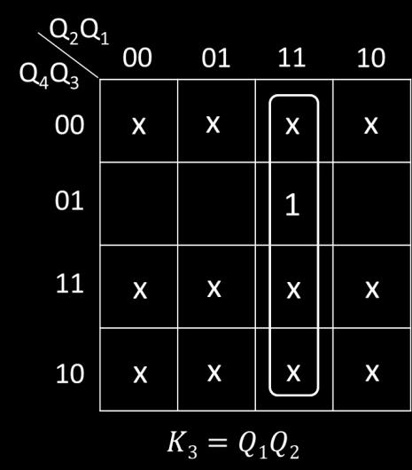
20 6 Synchronous State Machine Design Design a counter to generate the repetitive sequence 0,1,2,4,3,6. Step 1. Number of flip-flops: A counter with repetitive sequence 0, 1, 2, 4, 3, 6 requires 3 flip-flops. The counting sequence is 000, 001, 010, 100, 011, 110, 000 Step 2. Draw the state diagram: Step 3. Select the type of flip-flops and draw the excitation table: T flip-flops are selected and the excitation table of a given sequence counter using T flip-flops is shown below. PS NS Required excitations Q 3 Q 2 Q 1 Q 3 Q 2 Q 1 T 3 T 2 T Step 4. Obtain the minimal expressions K Maps for excitations T 3, T 2, and T 1 and their minimized form are as follows: T3 = Q3 + Q2 2


21 6 Synchronous State Machine Design T2 = Q3 + Q1Q2 + Q1 Q2 T1 = Q2 + Q1 Step 5. Draw the logic diagram Design 3-bit synchronous up counter using T flip flop. Step 1. Number of flip-flops: A 3 bit up counter requires 3 flip-flops. The counting sequence is 000, 001, 010, 011, 100, 101, 110, 111, 000 3

22 6 Synchronous State Machine Design Step 2. Draw the state diagram: Step 3. Select the type of flip-flops and draw the excitation table: T flip-flops are selected and the excitation table of a given sequence counter using T flip-flops is shown below. PS NS Required excitations Q 3 Q 2 Q 1 Q 3 Q 2 Q 1 T 3 T 2 T Step 4. Obtain the minimal expressions From excitation table, T 1 = 1. K Maps for excitations T 3 and T 2 and their minimized form are as follows: T2 = Q1 4

23 6 Synchronous State Machine Design Step 5. Draw the logic diagram T3 = Q1Q2 Design a synchronous BCD counter with JK flip-flops. Step 1. Number of flip-flops: A BCD counter requires 4 flip-flops. The counting sequence is 0000, 0001, 0010, 0011, 0100, 0101, 0110, 0111, 1000, 1001,
24 6 Synchronous State Machine Design Step 2. Draw the state diagram: Step 3. Select the type of flip-flops and draw the excitation table: J-K flip-flops are selected and the excitation table of a given sequence counter using J-K flip-flops is shown below. PS NS Required excitations Q 4 Q 3 Q 2 Q 1 Q 4 Q 3 Q 2 Q 1 J 4 K 4 J 3 K 3 J 2 K 2 J 1 K x 0 x 0 x 1 x x 0 x 1 X x x 0 x x 0 1 x x 1 x x 1 x x x 0 0 X 1 x x x 0 1 X x x x 0 x 0 1 x x x 1 x 1 x x 0 0 x 0 x 1 x x 1 0 x 0 x x 1 Step 4. Obtain the minimal expressions From excitation table, it is clear that J 1 = K 1 = 1 K Maps for excitations J 4, K 4, J 3, K 3, J 2, K 2, J 1 and K 1 and their minimized form are as follows: 6
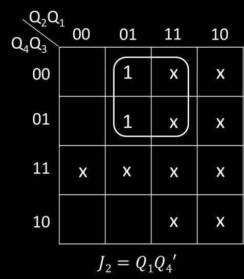
25 6 Synchronous State Machine Design 7

26 6 Synchronous State Machine Design Step 5. Draw the logic diagram Design a 3-bit synchronous up counter using K-maps and positive edgetriggered JK FFs. Step 1. Number of flip-flops: A 3 bit up counter requires 3 flip-flops. The counting sequence is 000, 001, 010, 011, 100, 101, 110, 111, 000 Step 2. Draw the state diagram: Step 3. Select the type of flip-flops and draw the excitation table: J-K flip-flops are selected and the excitation table of a given sequence counter using J-K flip-flops is shown below. PS NS Required excitations Q 3 Q 2 Q 1 Q 3 Q 2 Q 1 J 3 K 3 J 2 K 2 J 1 K x 0 x 1 x x 1 X x x x 0 1 x x x 1 x x 0 0 x 1 x x 0 1 x x x 0 x 0 1 x x 1 x 1 x 1 8


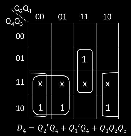
27 6 Synchronous State Machine Design Step 4. Obtain the minimal expressions From excitation table, J 1 = K 1 = 1. K Maps for excitations J 3, K 3, J 2 and K 2 and their minimized form are as follows: Step 5. Draw the logic diagram Design a mod-12 Synchronous up counter using D-flipflop. Step 1. Number of flip-flops: A mod-12 counter requires 4 flip-flops. The counting sequence is 0000, 0001, 0010, 0011, 0100, 0101, 0110, 0111, 1000, 1001, 1010, 1011,
28 6 Synchronous State Machine Design Step 2. Draw the state diagram: Step 3. Select the type of flip-flops and draw the excitation table: D flip-flops are selected and the excitation table of a given sequence counter using D flip-flops is shown below. PS NS Required excitations Q 4 Q 3 Q 2 Q 1 Q 4 Q 3 Q 2 Q 1 D 4 D 3 D 2 D Step 4. Obtain the minimal expressions K Maps for excitations D 4, D 3, D 2, and D 1 and their minimized form are as follows: 10
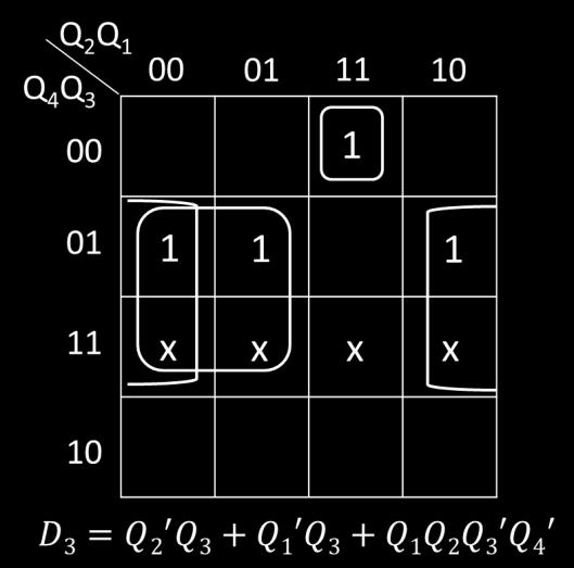
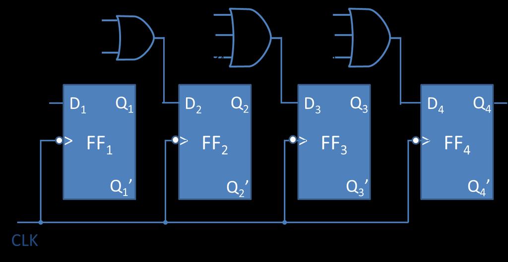
29 6 Synchronous State Machine Design Step 5. Draw the logic diagram 11


30 7 Asynchronous State Machines Fundamental-Mode Model An asynchronous system uses feedback to produce memory elements as does the synchronous state machine. The asynchronous machine generally uses gates rather than flip-flops. Figure demonstrates a simple asynchronous circuit. X and Y are the system inputs while Z is the system output. The signal Z is fed back, however, to a gate input and in this way helps determine its own value. When an X or Y change dictates a change in Z, this change occurs only after the cumulative propagation delay time through the gates. It is characteristic of asynchronous circuits that the feedback variables along with system inputs determine the values of these same feedback variables. An idealized model has been proposed to reflect this behavior. The above circuit is taken for the discussion. The gates are considered to have no delay in this model, while the delay element has an output that follows its input after a delay of Δt. The variable at the input of the delay element is called the excitation variable, while the feedback variable appears at the output of the delay element. In order to characterize the behavior of a circuit, we plot a map of excitation variable as a function of gate inputs. 1


31 7 Asynchronous State Machines It is important to realize that the value Z takes on will also be the value assumed by z after a delay of Δt. Thus, the information depicted by the map represents a dynamic situation. This can be demonstrated by supposing the system inputs are X = Y = 1 and z = 1, which leads to Z = 1. This is called a stable state since z = Z. If X is then changed to 0, the output Z changes to 0 as indicated by the map location corresponding to X = 0, Y = 1, and z = 1. This condition will persist for only Δt since z will assume a value of 0 at this time, moving the system to the X = 0, Y = 1, and z = 0 location. The location 011 is a transient state, while 010 is a stable state. The stable states are normally identified on the map by drawing a circle around the excitation variable such as in figure. Problems of Asynchronous Circuits Oscillation Problem If the system is in state a, a change of input from B = 0 to B = 1 sends the system to state c. State c is a transient state, and thus the excitation variable X changes to 1. A short time later x changes to 1, moving the system to state d. This state is also a transient state changing X back to 0, followed by a change in x to 0. The system now oscillates between states c and d. Of course, this type of situation can be used to advantage in a clock circuit by adding a delaying network to control the delay time Δt to create the desired oscillation frequency. In most systems, the oscillation is unacceptable, and the situation depicted by states c and d of the map must be avoided. Critical Race This situation can occur only when two or more feedback variables are present in the system. 2


32 7 Asynchronous State Machines This system has two external inputs, A and B, and two excitation variables, X and Y, that are fed back to the input of the circuit. One critical race occurs if the system starts in state e and input B changes from 1 to 0. The excitation variables begin to switch from XY = 00 toward XY = 11. Due to unequal propagation delays, one of the excitation variables will reach a value of 1 while the other has not changed from a value of 0. If the condition XY = 10 is reached, the system moves to stable state d. If the condition XY = 01 is reached rather than 10, the system moves to stable state b. The final stable state reached from this input condition depends on the relative switching speeds of variables X and Y. This situation is referred to as a critical race. 3
33 8 Logic Families Characteristics of Digital IC Threshold Voltage The threshold voltage is defined as that voltage at the input of a gate which causes a change in the state of the output from one logic level to the other. Propagation Delay A pulse through a gate takes a certain amount of time to propagate from input to output. This interval of time is known as the propagation delay of the gate. Power dissipation The power dissipation of a logic gate is the power required by the gate to operate with 50% duty cycle at a specified frequency and is expressed in mill watts. Fan-in The fan-in of a logic gate is defined as the number of inputs that the gate is designed to handle. Fan-out The fan-out (loading factor) of a logic gate is defined as the maximum number of standard loads that the output of the gate can drive without impairing its normal operation. Noise Margin When the digital circuits operate in noisy environment the gates may malfunction if the noise is beyond certain limits. The noise immunity of a logic circuit refers to the circuit s ability to tolerate noise voltages at its input. A quantitative measure of noise immunity is called noise margin. Operating temperatures The IC gates and other circuits are temperature sensitive being semiconductor devices. However they are designed to operate satisfactorily over a specified range of temperatures. The range specified for commercial applications is 0 to 70 C, for industrial it is 0 to 85 C and for military applications it is -55 C to 125 C. Speed Power Product A common means for measuring and comparing the overall performance of an IC family is the speed power product which is obtained by multiplying the gate propagation delay by the gate power dissipation. The smaller the product, the better the overall performance. Transistor-Transistor Logic (TTL) The TTL is so named because of its independence on transistors alone to perform basic logic operations. The TTL uses transistors operating in saturated mode. It is the fastest of saturated logic families. The basic TTL logic circuit is the NAND gate. Good speed, low manufacturing cost, wide range of circuits and the availability in SSI and MSI are its advantages. Tight V CC tolerance, relatively high power consumption, moderate packing density, generation of noise spikes and susceptibility to power transients are its disadvantages. TTL logic family consists of several subfamilies such as: 1
34 o o o o o o o o Standard TTL High Speed TTL Low Power TTL Schottky TTL Low Power Schottky TTL Advanced Schottky TTL Advanced Low Power Schottky TTL F (Fast) TTL For standard TTL, o Propagation Delay time = 9 ns o Power dissipation per = 10 mw o Noise Margin = 0.4 mv o Fan-in = 8 o Fan-out = 10 o Logic 0 = 0 V to 0.8 V o Logic 1 = 2 V to 5 V o Indeterminate Range = 0.8 V to 2 V Emitter-Coupled Logic (ECL) MOSFET This logic family is also called Current Mode Logic or Current Steering Logic. It is the fastest of all logic families. 8 Logic Families ECL operates on the principle of current switching, whereby a fixed bias current less than IC switched from one transistor s collector to another. Because of this mode operation, this logic form is also referred to as Current Mode Logic (CML). It is also called Current Steering Logic (CSL), because current is steered from one device to another. The ECL family is used in very high frequency applications where its speed is superior. The important characteristics of ECL are: o Transistors never saturate. So, speed is high o Logic Levels are negative, -0.9 V for Logic 1 and -1.7 V for Logic 0. o Noise Margin is less, about 250 mv. This makes ECL, unreliable for use in heavy industrial environment. o ECL circuits produce the output and its complement, and therefore, eliminate the need for inverters. o Fan-out is large because the output impedance is low. It is about 25. o Power dissipation per gate is large. o The total current flow in ECL is more or less constant. So, no noise spikes will be internally generated. MOSFET family are simpler & inexpensive to fabricate, require much less power, have better noise margin, a greater supply voltage range, a higher fan-out and require much less chip area as compared to other bipolar logic families. For MOS logic, o Propagation Delay, t pd = 50 ns. o Noise Margin, NM = 1.5 V. 2
35 8 Logic Families o Power Dissipation, PD = 0.1 Mw. o Fan out = 50 for frequencies greater than 100 Hz and it is virtually unlimited for dc or low frequencies. o The propagation delay associated with MOS gates is large (50 ns) because of their high output resistance (100 k) and capacitive loading presented by the driven gates. There are three types of MOSFET: o P-channel MOSFET (PMOS) Enhancement Type PMOS Depletion Type PMOS o N-channel MOSFET (NMOS) Enhancement Type NMOS Depletion Type NMOS o Complementary MOSFET (CMOS) Compare TTL, ECL, & CMOS logic families. Characteristic TTL CMSO ECL Power Input Moderate Low Moderate-High Frequency limit High Moderate Very high Circuit density Moderate-high High-very high Moderate Circuit types per family High High Moderate Logic Family Propagation delay time (ns) Power dissipation per gate (mw) Noise Margin (V) Fan-in Fan-out Cost TTL Low CMOS < Low ECL High CMOS NAND Gate Figure shows a CMOS two-input NAND gate and its equivalent circuits for various input combinations. 3
36 8 Logic Families Here Q 1 and Q 2 are parallel-connected PMOS transistors, and Q 3 and Q 4 are series-connected NMOS transistors. 4
37 8 Logic Families When A = 0 V and B = 0 V, V GS1 = V GS2 = -5 V, V GS3 = V GS4 = 0 V. So Q 1 is ON, Q 3 is OFF, Q 2 is ON and Q 4 is OFF. Thus, the switching circuit (b) results with V out = +5 V. When A = 0 V and B = +5 V, V GS1 = -5 V, V GS2 = 0 V, V GS3 = 0 V, V GS4 = 5 V. So Q 1 is ON, Q 3 is OFF, Q 2 is OFF and Q 4 is ON. Thus, the switching circuit (c) results with V out = +5 V. When A = +5 V and B = 0 V, V GS1 = 0 V, V GS2 = -5 V, V GS3 = 5 V, V GS4 = 0 V. So Q 1 is OFF, Q 3 is ON, Q 2 is ON and Q 4 is OFF. Thus, the switching circuit (d) results with V out = +5 V. When A = +5 V and B = +5 V, V GS1 = V GS2 = 0 V, V GS3 = V GS4 = 5 V. So Q 1 is OFF, Q 3 is ON, Q 2 is OFF and Q 4 is ON. Thus, the switching circuit (e) results with V out = 0 V. 5
38 9 Programmable Logic Devices Introduction to Programmable Logic Devices A programmable logic device is an IC that is user configurable and is capable of implementing logic functions. It is an LSI chip that contains a 'regular' structure and allows the designer to customize it for any specific application, i.e. it is programmed by the user to perform a function required for his application. A PLD contains a large number of gates, flip- flops, and registers that are interconnected on the chip. Many of the connections, however, are fusible links that can be broken. The IC is said to be programmable because the specific function of the IC for a given application is determined by the selective breaking of some of the interconnections while leaving others intact. The 'fuse blowing' process can be done either by the manufacturer in accordance with the customer's instructions, or by the customer himself which is called 'programming' because it produces the desired circuit pattern interconnecting the gates, flip-flops, registers, and so on. PLDs can be reprogrammed in a few seconds and hence give more flexibili ty to experiment with designs. The advantages of PLDs over fixed function ICs are as follows: 1. Low development cost 2. Less space requirement 3. Less power requirement 4. High reliability 5. Easy circuit testing 6. Easy design modification 7. High design security 8. Less design time 9. High switching speed Read Only Memory (ROM) A read-only memory (ROM) is essentially a memory device in which permanent binary information is stored. Once the pattern is established, it stays within the unit when the power is turned off and on again. ROMs are used to store information which is of fixed type, such as tables for various functions, fixed data and instructions. The advantages of using a ROM as a PLD are the following: 1. Ease of design since no simplification or minimization of logic function is required. 2. Designs can be changed, modified rapidly. 3. It is usually faster than discrete MSI/SSI circuit. 4. Cost is reduced. There are a few disadvantages also of ROM based circuits, such as: 1. Non-utilization of complete circuit 2. Increased power requirement 3. Enormous increase in size with increase in the number of input variables making it impractical 1
39 9 Programmable Logic Devices ROM Organization A block diagram of a ROM is shown in the figure. It consists of k inputs and n outputs. The inputs provide the address for the memory and the outputs give the data bits of the stored word which is selected by the address. The number of words in a ROM is determined from the fact that k address input lines are needed to specify 2k words. Consider, for example, a 32 x 8 ROM. The unit consists of 32 words of 8 bits each. There are five input lines that form the binary numbers from 0 through 31 for the address. The five inputs are decoded into 32 distinct outputs by means of a 5 x 32 decoder. ROM is basically a decoder with k inputs and 2k output lines followed by a bank of OR gates. Each output of the decoder represents a memory address. The 32 outputs of the decoder are connected to each of the 8 OR gates. Each OR gate must be considered as having 32 inputs. Since each OR gate has 32 input connections and there are 8 OR gates, the ROM contains 32 x 8 = 256 internal connections. In general, a 2k x n ROM will have an internal k x 2k decoder and n OR gates. Each OR gate has 2k inputs, which are connected to each of the outputs of the decoder. Types of ROM 2
40 9 Programmable Logic Devices Maskable programmable read-only memory (MROM) In this type of read-only memory, the user specifies the data to be stored to the manufacturer of the memory. The data pattern specified by the user are programmed as a part of the fabrication process. Once programmed, the data pattern can never be changed. This type of read-only memory is referred to as ROM. ROMs are highly suited for very high volume usage due to their low cost. Programmable read-only memory (PROM) This type of memory comes from the manufacturer without any data stored in it, i.e. empty. The data pattern is programmed electrically by the user using a special circuit known as PROM programmer. It can be programmed only once during its life time. Once programmed, the data cannot be altered. This type of memory is known as PROM. These are highly suited for high volume usage due to their low cost of production. Erasable programmable read-only memory (EPROM) In this type of memory, data can be written any number of times, i.e. they are reprogrammable. Before it is reprogrammed, the contents already stored are erased by exposing the chip to ultraviolet radiation for about 30 minutes. This type of memory is referred to as EPROM. EPROMs are possible only in MOS technology. Programming is done using a PROM programmer. Electrically erasable and programmable read-only memory (EEPROM or E2PROM) This is another type of reprogrammable memory in which erasing is done electrically rather than exposing the chip to the ultraviolet radiation. It is referred to as EEPROM or electrically alterable ROM (EAROM). PROGRAMMABLE ARRAY LOGIC (PAL) Programmable array logic (a registered trade mark of Monolithic Memories) is a particular family of programmable logic devices (PLDs) that is widely used and available from a number of manufacturers. The PAL circuits consist of a set of AND gates whose inputs can be programmed and whose outputs are connected to an OR gate, i.e. the inputs to the OR gate are hard-wired, i.e. PAL is a PLD with a fixed OR array and a programmable AND array. 3
41 9 Programmable Logic Devices Figure shows a small example of the basic structure. The fuse symbols represent fusible links that can be burned open using equipment similar to a PROM programmer. Figure shows how the circuit is programmed to implement F = A BC + AB C. All input variables and their complements are left connected to the unused AND gate, whose output is, therefore, AA BB CC = 0. The 0 has no effect on the output of the OR gate. The actual PAL circuits have several groups of AND gates, each group providing inputs to separate OR gates. 4
42 9 Programmable Logic Devices Figure shows an example of how the PAL structure is represented using the abbreviated connections. It is a 3-input 3-wide AND-OR structure. Each function can have three minterms or product terms. Inputs to the OR gates at the outputs are fixed as shown by x marked on the vertical lines. The inputs to the AND gates are marked on the corresponding line by the x. Removing the x implies blowing off the corresponding fuse which in turn implies that the corresponding input variable is not applied to the particular AND gate. Programmable Logic Array (PLA) The PLA combines the characteristics of the PROM and the PAL by providing both a programmable OR array and a programmable AND array, i.e. in a PLA both AND gates and OR gates have fuses at the inputs. A third set of fuses in the output inverters allows the output function to be inverted if required. Usually X-OR gates are used for controlled inversion. However, it has some disadvantages. Because it has two sets of fuses, it is more difficult to manufacture, program and test it than a PROM or a PAL. Figure demonstrates the structure of a three-input, four-output PLA with every fusible link intact. Like ROM, PLA can be mask programmable or field programmable. 5

43 9 Programmable Logic Devices With a mask programmable PLA, the user must submit a PLA programming table to the manufacturer. This table is used by the vender to produce a user made PLA that has the required internal paths between inputs and outputs. A second type of PLA available is called a field programmable logic array or FPLA. The FPLA can be programmed by the user by means of certain recommended procedures. FPLAs can be programmed with commercially available programmer units. Compare ROM, PAL and PLA ROM PAL PLA Consist of fixed AND gate array and programmable OR array. Consist of programmable AND gate array and programmable OR array. Consist of programmable AND gate array and programmable OR array. Medium speed High speed Slow Cheap Intermediate cost Most expensive Not flexible Not flexible Offering maximum programming flexibility It is possible to decode any minterms SOP function in the standard form only can be implemented We can get any desired minterms by programming the AND matrix Any SOP function can be implemented We can get any desired minterms by programming the AND & OR matrix Any SOP function can be implemented Xilinx FPGA The basic architecture is shown in figure. The logic modules have inputs and outputs that can be connected to metal lines by programmable switches. 6
44 9 Programmable Logic Devices The direct lines allow signals to be sent to or received from adjacent logic modules. These direct lines can also be programmed to connect to the general purpose interconnect lines to allow interconnection of nonadjacent logic modules if required. In addition, signals can be switched from one path to another at the intersections of rows and columns of the general purpose interconnect lines. A simplified diagram of the configurable logic block or CLB is shown in figure. This block is similar to a two flip-flop, RAM -controlled state machine. The combinational logic is performed by a RAM that can be used as a 32 x 1 or two 16 x 1 RAMs. 7
Section 3: Combinational Logic Design. Department of Electrical Engineering, University of Waterloo. Combinational Logic
 Section 3: Combinational Logic Design Major Topics Design Procedure Multilevel circuits Design with XOR gates Adders and Subtractors Binary parallel adder Decoders Encoders Multiplexers Programmed Logic
 vidyarthiplus.com vidyarthiplus.com vidyarthiplus.com ANNA UNIVERSITY- COMBATORE B.E./ B.TECH. DEGREE EXAMINATION - JUNE 2009. ELECTRICAL & ELECTONICS ENGG. - FOURTH SEMESTER DIGITAL LOGIC CIRCUITS PART-A
Vidyalankar S.E. Sem. III [CMPN] Digital Logic Design and Analysis Prelim Question Paper Solution
![Vidyalankar S.E. Sem. III [CMPN] Digital Logic Design and Analysis Prelim Question Paper Solution](/thumbs/90/103673562.jpg "Vidyalankar S.E. Sem. III [CMPN] Digital Logic Design and Analysis Prelim Question Paper Solution") . (a) (i) ( B C 5) H (A 2 B D) H S.E. Sem. III [CMPN] Digital Logic Design and Analysis Prelim Question Paper Solution ( B C 5) H (A 2 B D) H = (FFFF 698) H (ii) (2.3) 4 + (22.3) 4 2 2. 3 2. 3 2 3. 2 (2.3)
. (a) (i) ( B C 5) H (A 2 B D) H S.E. Sem. III [CMPN] Digital Logic Design and Analysis Prelim Question Paper Solution ( B C 5) H (A 2 B D) H = (FFFF 698) H (ii) (2.3) 4 + (22.3) 4 2 2. 3 2. 3 2 3. 2 (2.3)
LOGIC CIRCUITS. Basic Experiment and Design of Electronics. Ho Kyung Kim, Ph.D.
 Basic Experiment and Design of Electronics LOGIC CIRCUITS Ho Kyung Kim, Ph.D. hokyung@pusan.ac.kr School of Mechanical Engineering Pusan National University Digital IC packages TTL (transistor-transistor
Logic. Combinational. inputs. outputs. the result. system can
 Digital Electronics Combinational Logic Functions Digital logic circuits can be classified as either combinational or sequential circuits. A combinational circuit is one where the output at any time depends
MAHARASHTRA STATE BOARD OF TECHNICAL EDUCATION (Autonomous) (ISO/IEC Certified)
 (ISO/IEC Certified)") WINTER 17 EXAMINATION Subject Name: Digital Techniques Model Answer Subject Code: 17333 Important Instructions to examiners: 1) The answers should be examined by key words and not as word-to-word as given
WINTER 17 EXAMINATION Subject Name: Digital Techniques Model Answer Subject Code: 17333 Important Instructions to examiners: 1) The answers should be examined by key words and not as word-to-word as given
on candidate s understanding. 7) For programming language papers, credit may be given to any other program based on equivalent concept.
 For programming language papers, credit may be given to any other program based on equivalent concept.") WINTER 17 EXAMINATION Subject Name: Digital Techniques Model Answer Subject Code: 17333 Important Instructions to examiners: 1) The answers should be examined by key words and not as word-to-word as given
WINTER 17 EXAMINATION Subject Name: Digital Techniques Model Answer Subject Code: 17333 Important Instructions to examiners: 1) The answers should be examined by key words and not as word-to-word as given
COMBINATIONAL LOGIC FUNCTIONS
 COMBINATIONAL LOGIC FUNCTIONS Digital logic circuits can be classified as either combinational or sequential circuits. A combinational circuit is one where the output at any time depends only on the present
Sample Test Paper - I
 Scheme G Sample Test Paper - I Course Name : Computer Engineering Group Marks : 25 Hours: 1 Hrs. Q.1) Attempt any THREE: 09 Marks a) Define i) Propagation delay ii) Fan-in iii) Fan-out b) Convert the following:
KUMARAGURU COLLEGE OF TECHNOLOGY COIMBATORE
 Estd-1984 KUMARAGURU COLLEGE OF TECHNOLOGY COIMBATORE 641 006 QUESTION BANK UNIT I PART A ISO 9001:2000 Certified 1. Convert (100001110.010) 2 to a decimal number. 2. Find the canonical SOP for the function
( c) Give logic symbol, Truth table and circuit diagram for a clocked SR flip-flop. A combinational circuit is defined by the function
 Give logic symbol, Truth table and circuit diagram for a clocked SR flip-flop. A combinational circuit is defined by the function") Question Paper Digital Electronics (EE-204-F) MDU Examination May 2015 1. (a) represent (32)10 in (i) BCD 8421 code (ii) Excess-3 code (iii) ASCII code (b) Design half adder using only NAND gates. ( c)
Question Paper Digital Electronics (EE-204-F) MDU Examination May 2015 1. (a) represent (32)10 in (i) BCD 8421 code (ii) Excess-3 code (iii) ASCII code (b) Design half adder using only NAND gates. ( c)
Dept. of ECE, CIT, Gubbi Page 1
 Verification: 1) A.B = A + B 7404 7404 7404 A B A.B A.B 0 0 0 1 0 1 0 1 1 0 0 1 1 1 1 0 A B A B A + B 0 0 1 1 1 0 1 1 0 1 1 0 0 1 1 1 1 0 0 0 2) A+B = A. B 7404 7404 7404 A B A+B A+B 0 0 0 1 0 1 1 0 1
Department of Electrical & Electronics EE-333 DIGITAL SYSTEMS
 Department of Electrical & Electronics EE-333 DIGITAL SYSTEMS 1) Given the two binary numbers X = 1010100 and Y = 1000011, perform the subtraction (a) X -Y and (b) Y - X using 2's complements. a) X = 1010100
LOGIC CIRCUITS. Basic Experiment and Design of Electronics
 Basic Experiment and Design of Electronics LOGIC CIRCUITS Ho Kyung Kim, Ph.D. hokyung@pusan.ac.kr School of Mechanical Engineering Pusan National University Outline Combinational logic circuits Output
DIGITAL LOGIC CIRCUITS
 DIGITAL LOGIC CIRCUITS Introduction Logic Gates Boolean Algebra Map Specification Combinational Circuits Flip-Flops Sequential Circuits Memory Components Integrated Circuits Digital Computers 2 LOGIC GATES
Reg. No. Question Paper Code : B.E./B.Tech. DEGREE EXAMINATION, NOVEMBER/DECEMBER Second Semester. Computer Science and Engineering
 Sp 6 Reg. No. Question Paper Code : 27156 B.E./B.Tech. DEGREE EXAMINATION, NOVEMBER/DECEMBER 2015. Second Semester Computer Science and Engineering CS 6201 DIGITAL PRINCIPLES AND SYSTEM DESIGN (Common
SUMMER 18 EXAMINATION Subject Name: Principles of Digital Techniques Model Answer Subject Code:
 Important Instructions to examiners: 1) The answers should be examined by key words and not as word-to-word as given in the model answer scheme. 2) The model answer and the answer written by candidate
Show that the dual of the exclusive-or is equal to its compliment. 7
 Darshan Institute of ngineering and Technology, Rajkot, Subject: Digital lectronics (2300) GTU Question ank Unit Group Questions Do as directed : I. Given that (6)0 = (00)x, find the value of x. II. dd
Digital Electronics Circuits 2017
 JSS SCIENCE AND TECHNOLOGY UNIVERSITY Digital Electronics Circuits (EC37L) Lab in-charge: Dr. Shankraiah Course outcomes: After the completion of laboratory the student will be able to, 1. Simplify, design
S.Y. Diploma : Sem. III [DE/ED/EI/EJ/EN/ET/EV/EX/IC/IE/IS/IU/MU] Principles of Digital Techniques
![S.Y. Diploma : Sem. III [DE/ED/EI/EJ/EN/ET/EV/EX/IC/IE/IS/IU/MU] Principles of Digital Techniques](/thumbs/82/86792063.jpg "S.Y. Diploma : Sem. III [DE/ED/EI/EJ/EN/ET/EV/EX/IC/IE/IS/IU/MU] Principles of Digital Techniques") S.Y. Diploma : Sem. III [DE/ED/EI/EJ/EN/ET/EV/EX/IC/IE/IS/IU/MU] Principles of Digital Techniques Time: 3 Hrs.] Prelim Question Paper Solution [Marks : 100 Q.1(a) Attempt any SIX of the following : [12]
S.Y. Diploma : Sem. III [DE/ED/EI/EJ/EN/ET/EV/EX/IC/IE/IS/IU/MU] Principles of Digital Techniques Time: 3 Hrs.] Prelim Question Paper Solution [Marks : 100 Q.1(a) Attempt any SIX of the following : [12]
DHANALAKSHMI COLLEGE OF ENGINEERING, CHENNAI DEPARTMENT OF COMPUTER SCIENCE AND ENGINEERING CS6201 DIGITAL PRINCIPLES AND SYSTEM DESIGN
 DHANALAKSHMI COLLEGE OF ENGINEERING, CHENNAI DEPARTMENT OF COMPUTER SCIENCE AND ENGINEERING CS6201 DIGITAL PRINCIPLES AND SYSTEM DESIGN UNIT I : BOOLEAN ALGEBRA AND LOGIC GATES PART - A (2 MARKS) Number
UNIT II COMBINATIONAL CIRCUITS:
 UNIT II COMBINATIONAL CIRCUITS: INTRODUCTION: The digital system consists of two types of circuits, namely (i) (ii) Combinational circuits Sequential circuits Combinational circuit consists of logic gates
CS470: Computer Architecture. AMD Quad Core
 CS470: Computer Architecture Yashwant K. Malaiya, Professor malaiya@cs.colostate.edu AMD Quad Core 1 Architecture Layers Building blocks Gates, flip-flops Functional bocks: Combinational, Sequential Instruction
S No. Questions Bloom s Taxonomy Level UNIT-I
 GROUP-A (SHORT ANSWER QUESTIONS) S No. Questions Bloom s UNIT-I 1 Define oxidation & Classify different types of oxidation Remember 1 2 Explain about Ion implantation Understand 1 3 Describe lithography
ECEN 248: INTRODUCTION TO DIGITAL SYSTEMS DESIGN. Week 9 Dr. Srinivas Shakkottai Dept. of Electrical and Computer Engineering
 ECEN 248: INTRODUCTION TO DIGITAL SYSTEMS DESIGN Week 9 Dr. Srinivas Shakkottai Dept. of Electrical and Computer Engineering TIMING ANALYSIS Overview Circuits do not respond instantaneously to input changes
Systems I: Computer Organization and Architecture
 Systems I: Computer Organization and Architecture Lecture 6 - Combinational Logic Introduction A combinational circuit consists of input variables, logic gates, and output variables. The logic gates accept
SAU1A FUNDAMENTALS OF DIGITAL COMPUTERS
 SAU1A FUNDAMENTALS OF DIGITAL COMPUTERS Unit : I - V Unit : I Overview Fundamentals of Computers Characteristics of Computers Computer Language Operating Systems Generation of Computers 2 Definition of
CPE/EE 422/522. Chapter 1 - Review of Logic Design Fundamentals. Dr. Rhonda Kay Gaede UAH. 1.1 Combinational Logic
 CPE/EE 422/522 Chapter - Review of Logic Design Fundamentals Dr. Rhonda Kay Gaede UAH UAH Chapter CPE/EE 422/522. Combinational Logic Combinational Logic has no control inputs. When the inputs to a combinational
DIGITAL LOGIC CIRCUITS
 DIGITAL LOGIC CIRCUITS Introduction Logic Gates Boolean Algebra Map Specification Combinational Circuits Flip-Flops Sequential Circuits Memor Components Integrated Circuits BASIC LOGIC BLOCK - GATE - Logic
S.Y. Diploma : Sem. III [CO/CM/IF/CD/CW] Digital Techniques s complement 2 s complement 1 s complement
![S.Y. Diploma : Sem. III [CO/CM/IF/CD/CW] Digital Techniques s complement 2 s complement 1 s complement](/thumbs/80/82077570.jpg "S.Y. Diploma : Sem. III [CO/CM/IF/CD/CW] Digital Techniques s complement 2 s complement 1 s complement") S.Y. Diploma : Sem. III [CO/CM/IF/CD/CW] Digital Techniques Time: 3 Hrs.] Prelim Question Paper Solution [Marks : Q.(a) (i) () (2) s COMPLEMENT s COMPLEMENT 2s COMPLEMENT 2s COMPLEMENT + Q.(a) (ii) ()
S.Y. Diploma : Sem. III [CO/CM/IF/CD/CW] Digital Techniques Time: 3 Hrs.] Prelim Question Paper Solution [Marks : Q.(a) (i) () (2) s COMPLEMENT s COMPLEMENT 2s COMPLEMENT 2s COMPLEMENT + Q.(a) (ii) ()
Vidyalankar S.E. Sem. III [EXTC] Digital Electronics Prelim Question Paper Solution ABCD ABCD ABCD ABCD ABCD ABCD ABCD ABCD = B
![Vidyalankar S.E. Sem. III [EXTC] Digital Electronics Prelim Question Paper Solution ABCD ABCD ABCD ABCD ABCD ABCD ABCD ABCD = B](/thumbs/84/91058397.jpg "Vidyalankar S.E. Sem. III [EXTC] Digital Electronics Prelim Question Paper Solution ABCD ABCD ABCD ABCD ABCD ABCD ABCD ABCD = B") . (a). (b). (c) S.E. Sem. III [EXTC] igital Electronics Prelim Question Paper Solution ABC ABC ABC ABC ABC ABC ABC ABC = B LHS = ABC ABC ABC ABC ABC ABC ABC ABC But ( ) = = ABC( ) ABC( ) ABC( ) ABC( )
. (a). (b). (c) S.E. Sem. III [EXTC] igital Electronics Prelim Question Paper Solution ABC ABC ABC ABC ABC ABC ABC ABC = B LHS = ABC ABC ABC ABC ABC ABC ABC ABC But ( ) = = ABC( ) ABC( ) ABC( ) ABC( )
TYPICAL QUESTIONS & ANSWERS
 TYPICAL QUESTIONS & ANSWERS PART - I OJECTIVE TYPE QUESTIONS Each Question carries 2 marks. Choose correct or the best alternative in the following: Q.1 The NAN gate output will be low if the two inputs
MAHARASHTRA STATE BOARD OF TECHNICAL EDUCATION (Autonomous) (ISO/IEC Certified) State any two Boolean laws. (Any 2 laws 1 mark each)
 (ISO/IEC Certified) State any two Boolean laws. (Any 2 laws 1 mark each)") Subject Code: 17333 Model Answer Page 1/ 27 Important Instructions to examiners: 1) The answers should be examined by key words and not as word-to-word as given in the model answer scheme. 2) The model
Subject Code: 17333 Model Answer Page 1/ 27 Important Instructions to examiners: 1) The answers should be examined by key words and not as word-to-word as given in the model answer scheme. 2) The model
Unit II Chapter 4:- Digital Logic Contents 4.1 Introduction... 4
 Unit II Chapter 4:- Digital Logic Contents 4.1 Introduction... 4 4.1.1 Signal... 4 4.1.2 Comparison of Analog and Digital Signal... 7 4.2 Number Systems... 7 4.2.1 Decimal Number System... 7 4.2.2 Binary
CMOS Digital Integrated Circuits Lec 13 Semiconductor Memories
 Lec 13 Semiconductor Memories 1 Semiconductor Memory Types Semiconductor Memories Read/Write (R/W) Memory or Random Access Memory (RAM) Read-Only Memory (ROM) Dynamic RAM (DRAM) Static RAM (SRAM) 1. Mask
MAHARASHTRA STATE BOARD OF TECHNICAL EDUCATION
 MAHARASHTRA STATE BOARD OF TECHNICAL EDUCATION (Autonomous) (ISO/IEC - 27001-2005 Certified) Subject Code: 12069 SUMMER 13 EXAMINATION Model Answer Important Instructions to examiners: 1) The answers should
S.Y. Diploma : Sem. III [CO/CM/IF/CD/CW] Digital Techniques
![S.Y. Diploma : Sem. III [CO/CM/IF/CD/CW] Digital Techniques](/thumbs/90/103932933.jpg "S.Y. Diploma : Sem. III [CO/CM/IF/CD/CW] Digital Techniques") S.Y. Diploma : Sem. III [CO/CM/IF/CD/CW] Digital Techniques Time: 3 Hrs.] Prelim Question Paper Solution [Marks : 100 Q.1(a) Attempt any SIX of the following : [12] Q.1(a) (i) Derive AND gate and OR gate
S.Y. Diploma : Sem. III [CO/CM/IF/CD/CW] Digital Techniques Time: 3 Hrs.] Prelim Question Paper Solution [Marks : 100 Q.1(a) Attempt any SIX of the following : [12] Q.1(a) (i) Derive AND gate and OR gate
King Fahd University of Petroleum and Minerals College of Computer Science and Engineering Computer Engineering Department
 King Fahd University of Petroleum and Minerals College of Computer Science and Engineering Computer Engineering Department Page 1 of 13 COE 202: Digital Logic Design (3-0-3) Term 112 (Spring 2012) Final
Digital Logic. CS211 Computer Architecture. l Topics. l Transistors (Design & Types) l Logic Gates. l Combinational Circuits.
 l Logic Gates. l Combinational Circuits.") CS211 Computer Architecture Digital Logic l Topics l Transistors (Design & Types) l Logic Gates l Combinational Circuits l K-Maps Figures & Tables borrowed from:! http://www.allaboutcircuits.com/vol_4/index.html!
CS211 Computer Architecture Digital Logic l Topics l Transistors (Design & Types) l Logic Gates l Combinational Circuits l K-Maps Figures & Tables borrowed from:! http://www.allaboutcircuits.com/vol_4/index.html!
Programmable Logic Devices
 Programmable Logic Devices Mohammed Anvar P.K AP/ECE Al-Ameen Engineering College PLDs Programmable Logic Devices (PLD) General purpose chip for implementing circuits Can be customized using programmable
The Design Procedure. Output Equation Determination - Derive output equations from the state table
 The Design Procedure Specification Formulation - Obtain a state diagram or state table State Assignment - Assign binary codes to the states Flip-Flop Input Equation Determination - Select flipflop types
Review for B33DV2-Digital Design. Digital Design
 Review for B33DV2 The Elements of Modern Behaviours Design Representations Blocks Waveforms Gates Truth Tables Boolean Algebra Switches Rapid Prototyping Technologies Circuit Technologies TTL MOS Simulation
6 Synchronous State Machine Design
 Design of synchronous counters. Based on the description of the problem, determine the required number n of the FFs - the smallest value of n is such that the number of states N 2 n and the desired counting
EE40 Lec 15. Logic Synthesis and Sequential Logic Circuits
 EE40 Lec 15 Logic Synthesis and Sequential Logic Circuits Prof. Nathan Cheung 10/20/2009 Reading: Hambley Chapters 7.4-7.6 Karnaugh Maps: Read following before reading textbook http://www.facstaff.bucknell.edu/mastascu/elessonshtml/logic/logic3.html
KINGS COLLEGE OF ENGINEERING DEPARTMENT OF ELECTRONICS AND COMMUNICATION ENGINEERING QUESTION BANK
 KINGS COLLEGE OF ENGINEERING DEPARTMENT OF ELECTRONICS AND COMMUNICATION ENGINEERING QUESTION BANK SUBJECT CODE: EC 1354 SUB.NAME : VLSI DESIGN YEAR / SEMESTER: III / VI UNIT I MOS TRANSISTOR THEORY AND
EC-121 Digital Logic Design
 EC-121 Digital Logic Design Lecture 2 [Updated on 02-04-18] Boolean Algebra and Logic Gates Dr Hashim Ali Spring 2018 Department of Computer Science and Engineering HITEC University Taxila!1 Overview What
Boolean Algebra and Digital Logic 2009, University of Colombo School of Computing
 IT 204 Section 3.0 Boolean Algebra and Digital Logic Boolean Algebra 2 Logic Equations to Truth Tables X = A. B + A. B + AB A B X 0 0 0 0 3 Sum of Products The OR operation performed on the products of
ELECTRONICS & COMMUNICATION ENGINEERING PROFESSIONAL ETHICS AND HUMAN VALUES
 EC 216(R-15) Total No. of Questions :09] [Total No. of Pages : 02 II/IV B.Tech. DEGREE EXAMINATIONS, DECEMBER- 2016 First Semester ELECTRONICS & COMMUNICATION ENGINEERING PROFESSIONAL ETHICS AND HUMAN
DE58/DC58 LOGIC DESIGN DEC 2014
 Q.2 a. In a base-5 number system, 3 digit representations is used. Find out (i) Number of distinct quantities that can be represented.(ii) Representation of highest decimal number in base-5. Since, r=5
ELEC Digital Logic Circuits Fall 2014 Sequential Circuits (Chapter 6) Finite State Machines (Ch. 7-10)
 Finite State Machines (Ch. 7-10)") ELEC 2200-002 Digital Logic Circuits Fall 2014 Sequential Circuits (Chapter 6) Finite State Machines (Ch. 7-10) Vishwani D. Agrawal James J. Danaher Professor Department of Electrical and Computer Engineering
ELEC 2200-002 Digital Logic Circuits Fall 2014 Sequential Circuits (Chapter 6) Finite State Machines (Ch. 7-10) Vishwani D. Agrawal James J. Danaher Professor Department of Electrical and Computer Engineering
MAHARASHTRA STATE BOARD OF TECHNICAL EDUCATION (Autonomous) (ISO/IEC Certified) SUMMER 14 EXAMINATION Model Answer
 (ISO/IEC Certified) SUMMER 14 EXAMINATION Model Answer") MAHARASHTRA STATE BOARD OF TECHNICAL EDUCATION (Autonomous) (ISO/IEC 27001 2005 Certified) SUMMER 14 EXAMINATION Model Answer Subject Code : 17320 Page No: 1/34 Important Instructions to examiners: 1)
MAHARASHTRA STATE BOARD OF TECHNICAL EDUCATION (Autonomous) (ISO/IEC 27001 2005 Certified) SUMMER 14 EXAMINATION Model Answer Subject Code : 17320 Page No: 1/34 Important Instructions to examiners: 1)
King Fahd University of Petroleum and Minerals College of Computer Science and Engineering Computer Engineering Department
 King Fahd University of Petroleum and Minerals College of Computer Science and Engineering Computer Engineering Department Page of COE 22: Digital Logic Design (3--3) Term (Fall 22) Final Exam Sunday January
Adders, subtractors comparators, multipliers and other ALU elements
 CSE4: Components and Design Techniques for Digital Systems Adders, subtractors comparators, multipliers and other ALU elements Adders 2 Circuit Delay Transistors have instrinsic resistance and capacitance
SIR C.R.REDDY COLLEGE OF ENGINEERING ELURU DIGITAL INTEGRATED CIRCUITS (DIC) LABORATORY MANUAL III / IV B.E. (ECE) : I - SEMESTER
 LABORATORY MANUAL III / IV B.E. (ECE) : I - SEMESTER") SIR C.R.REDDY COLLEGE OF ENGINEERING ELURU 534 007 DIGITAL INTEGRATED CIRCUITS (DIC) LABORATORY MANUAL III / IV B.E. (ECE) : I - SEMESTER DEPARTMENT OF ELECTRONICS AND COMMUNICATION ENGINEERING DIGITAL
SIR C.R.REDDY COLLEGE OF ENGINEERING ELURU 534 007 DIGITAL INTEGRATED CIRCUITS (DIC) LABORATORY MANUAL III / IV B.E. (ECE) : I - SEMESTER DEPARTMENT OF ELECTRONICS AND COMMUNICATION ENGINEERING DIGITAL
PG - TRB UNIT-X- DIGITAL ELECTRONICS. POLYTECHNIC-TRB MATERIALS
 SRIMAAN COACHING CENTRE-PG-TRB-PHYSICS- DIGITAL ELECTRONICS-STUDY MATERIAL-CONTACT: 8072230063 SRIMAAN PG - TRB PHYSICS UNIT-X- DIGITAL ELECTRONICS POLYTECHNIC-TRB MATERIALS MATHS/COMPUTER SCIENCE/IT/ECE/EEE
Boolean Algebra. Digital Logic Appendix A. Postulates, Identities in Boolean Algebra How can I manipulate expressions?
 Digital Logic Appendix A Gates Combinatorial Circuits Sequential Circuits Other operations NAND A NAND B = NOT ( A ANDB) = AB NOR A NOR B = NOT ( A ORB) = A + B Truth tables What is the result of the operation
Chapter 2 Boolean Algebra and Logic Gates
 Chapter 2 Boolean Algebra and Logic Gates The most common postulates used to formulate various algebraic structures are: 1. Closure. N={1,2,3,4 }, for any a,b N we obtain a unique c N by the operation
Design of Sequential Circuits
 Design of Sequential Circuits Seven Steps: Construct a state diagram (showing contents of flip flop and inputs with next state) Assign letter variables to each flip flop and each input and output variable
Ch 9. Sequential Logic Technologies. IX - Sequential Logic Technology Contemporary Logic Design 1
 Ch 9. Sequential Logic Technologies Technology Contemporary Logic Design Overview Basic Sequential Logic Components FSM Design with Counters FSM Design with Programmable Logic FSM Design with More Sophisticated
Vidyalankar S.E. Sem. III [ETRX] Digital Circuits and Design Prelim Question Paper Solution
![Vidyalankar S.E. Sem. III [ETRX] Digital Circuits and Design Prelim Question Paper Solution](/thumbs/79/79145081.jpg "Vidyalankar S.E. Sem. III [ETRX] Digital Circuits and Design Prelim Question Paper Solution") S.E. Sem. III [ETRX] Digital Circuits and Design Prelim uestion Paper Solution. (a) Static Hazard Static hazards have two cases: static and static. static- hazard exists when the output variable should
S.E. Sem. III [ETRX] Digital Circuits and Design Prelim uestion Paper Solution. (a) Static Hazard Static hazards have two cases: static and static. static- hazard exists when the output variable should
 Distributed by: www.jameco.com 1-800-831-4242 The content and copyrights of the attached material are the property of its owner. DS0026 Dual High-Speed MOS Driver General Description DS0026 is a low cost
MM74C90 MM74C93 4-Bit Decade Counter 4-Bit Binary Counter
 4-Bit Decade Counter 4-Bit Binary Counter General Description The MM74C90 decade counter and the MM74C93 binary counter and complementary MOS (CMOS) integrated circuits constructed with N- and P-channel
Digital Logic Appendix A
 Digital Logic Appendix A Boolean Algebra Gates Combinatorial Circuits Sequential Circuits 1 Boolean Algebra George Boole ideas 1854 Claude Shannon, apply to circuit design, 1938 Describe digital circuitry
CHAPTER 7. Exercises 17/ / /2 2 0
 CHAPTER 7 Exercises E7. (a) For the whole part, we have: Quotient Remainders 23/2 /2 5 5/2 2 2/2 0 /2 0 Reading the remainders in reverse order, we obtain: 23 0 = 0 2 For the fractional part we have 2
CHW 261: Logic Design
 CHW 26: Logic Design Instructors: Prof. Hala Zayed Dr. Ahmed Shalaby http://www.bu.edu.eg/staff/halazayed4 http://bu.edu.eg/staff/ahmedshalaby4# Slide Digital Fundamentals Digital Concepts Slide 2 What?
Boolean Algebra. Digital Logic Appendix A. Boolean Algebra Other operations. Boolean Algebra. Postulates, Identities in Boolean Algebra
 Digital Logic Appendix A Gates Combinatorial Circuits Sequential Circuits George Boole ideas 1854 Claude Shannon, apply to circuit design, 1938 (piirisuunnittelu) Describe digital circuitry function programming
Chapter 7 Logic Circuits
 Chapter 7 Logic Circuits Goal. Advantages of digital technology compared to analog technology. 2. Terminology of Digital Circuits. 3. Convert Numbers between Decimal, Binary and Other forms. 5. Binary
Analog & Digital Electronics Laboratory. Code - CS391. Lab Manual
 Analog & Digital Electronics Laboratory Code - CS391 Lab Manual EXPERIMENT: 1 LOGIC GATES AIM: To study and verify the truth table of logic gates LEARNING OBJECTIVE: Identify various ICs and their specification.
Adders, subtractors comparators, multipliers and other ALU elements
 CSE4: Components and Design Techniques for Digital Systems Adders, subtractors comparators, multipliers and other ALU elements Instructor: Mohsen Imani UC San Diego Slides from: Prof.Tajana Simunic Rosing
S.E. Sem. III [ETRX] Digital Circuit Design. t phl. Fig.: Input and output voltage waveforms to define propagation delay times.
![S.E. Sem. III [ETRX] Digital Circuit Design. t phl. Fig.: Input and output voltage waveforms to define propagation delay times.](/thumbs/93/111090909.jpg "S.E. Sem. III [ETRX] Digital Circuit Design. t phl. Fig.: Input and output voltage waveforms to define propagation delay times.") S.E. Sem. III [ETRX] Digital ircuit Design Time : 3 Hrs.] Prelim Paper Solution [Marks : 80. Solve following : [20].(a) Explain characteristics of logic families. [5] haracteristics of logic families are
S.E. Sem. III [ETRX] Digital ircuit Design Time : 3 Hrs.] Prelim Paper Solution [Marks : 80. Solve following : [20].(a) Explain characteristics of logic families. [5] haracteristics of logic families are
WORKBOOK. Try Yourself Questions. Electrical Engineering Digital Electronics. Detailed Explanations of
 27 WORKBOOK Detailed Eplanations of Try Yourself Questions Electrical Engineering Digital Electronics Number Systems and Codes T : Solution Converting into decimal number system 2 + 3 + 5 + 8 2 + 4 8 +
Software Engineering 2DA4. Slides 8: Multiplexors and More
 Software Engineering 2DA4 Slides 8: Multiplexors and More Dr. Ryan Leduc Department of Computing and Software McMaster University Material based on S. Brown and Z. Vranesic, Fundamentals of Digital Logic
IT T35 Digital system desigm y - ii /s - iii
 UNIT - II Combinational Logic Adders subtractors code converters binary parallel adder decimal adder magnitude comparator encoders decoders multiplexers demultiplexers-binarymultiplier Parity generator
Lecture A: Logic Design and Gates
 Lecture A: Logic Design and Gates Syllabus My office hours 9.15-10.35am T,Th or gchoi@ece.tamu.edu 333G WERC Text: Brown and Vranesic Fundamentals of Digital Logic,» Buy it.. Or borrow it» Other book:
EE141Microelettronica. CMOS Logic
 Microelettronica CMOS Logic CMOS logic Power consumption in CMOS logic gates Where Does Power Go in CMOS? Dynamic Power Consumption Charging and Discharging Capacitors Short Circuit Currents Short Circuit
CMPE12 - Notes chapter 1. Digital Logic. (Textbook Chapter 3)
") CMPE12 - Notes chapter 1 Digital Logic (Textbook Chapter 3) Transistor: Building Block of Computers Microprocessors contain TONS of transistors Intel Montecito (2005): 1.72 billion Intel Pentium 4 (2000):
CMPE12 - Notes chapter 1 Digital Logic (Textbook Chapter 3) Transistor: Building Block of Computers Microprocessors contain TONS of transistors Intel Montecito (2005): 1.72 billion Intel Pentium 4 (2000):
Chapter 4. Combinational: Circuits with logic gates whose outputs depend on the present combination of the inputs. elements. Dr.
 Chapter 4 Dr. Panos Nasiopoulos Combinational: Circuits with logic gates whose outputs depend on the present combination of the inputs. Sequential: In addition, they include storage elements Combinational
KINGS COLLEGE OF ENGINEERING PUNALKULAM. DEPARTMENT OF ELECTRONICS AND COMMUNICATION ENGINEERING QUESTION BANK
 KINGS COLLEGE OF ENGINEERING PUNALKULAM. DEPARTMENT OF ELECTRONICS AND COMMUNICATION ENGINEERING QUESTION BANK SUBJECT CODE : EC1401 SEM / YEAR : VII/ IV SUBJECT NAME : VLSI DESIGN UNIT I CMOS TECHNOLOGY
Philadelphia University Student Name: Student Number:
 Philadelphia University Student Name: Student Number: Faculty of Engineering Serial Number: Final Exam, Second Semester: 2015/2016 Dept. of Computer Engineering Course Title: Logic Circuits Date: 08/06/2016
Memory, Latches, & Registers
 Memory, Latches, & Registers 1) Structured Logic Arrays 2) Memory Arrays 3) Transparent Latches 4) How to save a few bucks at toll booths 5) Edge-triggered Registers L13 Memory 1 General Table Lookup Synthesis
MOSIS REPORT. Spring MOSIS Report 1. MOSIS Report 2. MOSIS Report 3
 MOSIS REPORT Spring 2010 MOSIS Report 1 MOSIS Report 2 MOSIS Report 3 MOSIS Report 1 Design of 4-bit counter using J-K flip flop I. Objective The purpose of this project is to design one 4-bit counter
Chap 2. Combinational Logic Circuits
 Overview 2 Chap 2. Combinational Logic Circuits Spring 24 Part Gate Circuits and Boolean Equations Binary Logic and Gates Boolean Algebra Standard Forms Part 2 Circuit Optimization Two-Level Optimization
MODEL ANSWER SUMMER 17 EXAMINATION Subject Title: Principles of Digital Techniques
 MODEL ANSWER SUMMER 17 EXAMINATION Subject Title: Principles of Digital Techniques Subject Code: Important Instructions to examiners: 1) The answers should be examined by key words and not as word-to-word
Semiconductor Memories
 Introduction Classification of Memory Devices "Combinational Logic" Read Write Memories Non Volatile RWM Read Only Memory Random Access Non-Random Access Static RAM FIFO Dynamic RAM LIFO Shift Register
Binary addition (1-bit) P Q Y = P + Q Comments Carry = Carry = Carry = Carry = 1 P Q
 P Q Y = P + Q Comments Carry = Carry = Carry = Carry = 1 P Q") Digital Arithmetic In Chapter 2, we have discussed number systems such as binary, hexadecimal, decimal, and octal. We have also discussed sign representation techniques, for example, sign-bit representation
Digital Arithmetic In Chapter 2, we have discussed number systems such as binary, hexadecimal, decimal, and octal. We have also discussed sign representation techniques, for example, sign-bit representation
Fundamentals of Boolean Algebra
 UNIT-II 1 Fundamentals of Boolean Algebra Basic Postulates Postulate 1 (Definition): A Boolean algebra is a closed algebraic system containing a set K of two or more elements and the two operators and
Vidyalankar. S.E. Sem. III [EXTC] Digital System Design. Q.1 Solve following : [20] Q.1(a) Explain the following decimals in gray code form
![Vidyalankar. S.E. Sem. III [EXTC] Digital System Design. Q.1 Solve following : [20] Q.1(a) Explain the following decimals in gray code form](/thumbs/96/126594189.jpg "Vidyalankar. S.E. Sem. III [EXTC] Digital System Design. Q.1 Solve following : [20] Q.1(a) Explain the following decimals in gray code form") S.E. Sem. III [EXTC] Digital System Design Time : 3 Hrs.] Prelim Paper Solution [Marks : 80 Q.1 Solve following : [20] Q.1(a) Explain the following decimals in gray code form [5] (i) (42) 10 (ii) (17)
S.E. Sem. III [EXTC] Digital System Design Time : 3 Hrs.] Prelim Paper Solution [Marks : 80 Q.1 Solve following : [20] Q.1(a) Explain the following decimals in gray code form [5] (i) (42) 10 (ii) (17)
Synchronous Sequential Circuit
 Synchronous Sequential Circuit The change of internal state occurs in response to the synchronized clock pulses. Data are read during the clock pulse (e.g. rising-edge triggered) It is supposed to wait
Topics. Dynamic CMOS Sequential Design Memory and Control. John A. Chandy Dept. of Electrical and Computer Engineering University of Connecticut
 Topics Dynamic CMOS Sequential Design Memory and Control Dynamic CMOS In static circuits at every point in time (except when switching) the output is connected to either GND or V DD via a low resistance
MODULAR CIRCUITS CHAPTER 7
 CHAPTER 7 MODULAR CIRCUITS A modular circuit is a digital circuit that performs a specific function or has certain usage. The modular circuits to be introduced in this chapter are decoders, encoders, multiplexers,
Digital Integrated Circuits A Design Perspective
 Semiconductor Memories Adapted from Chapter 12 of Digital Integrated Circuits A Design Perspective Jan M. Rabaey et al. Copyright 2003 Prentice Hall/Pearson Outline Memory Classification Memory Architectures
Class Website:
 ECE 20B, Winter 2003 Introduction to Electrical Engineering, II LECTURE NOTES #5 Instructor: Andrew B. Kahng (lecture) Email: abk@ece.ucsd.edu Telephone: 858-822-4884 office, 858-353-0550 cell Office:
Lecture 22 Chapters 3 Logic Circuits Part 1
 Lecture 22 Chapters 3 Logic Circuits Part 1 LC-3 Data Path Revisited How are the components Seen here implemented? 5-2 Computing Layers Problems Algorithms Language Instruction Set Architecture Microarchitecture
Combinational Logic Design Combinational Functions and Circuits
 Combinational Logic Design Combinational Functions and Circuits Overview Combinational Circuits Design Procedure Generic Example Example with don t cares: BCD-to-SevenSegment converter Binary Decoders
Digital Logic: Boolean Algebra and Gates. Textbook Chapter 3
 Digital Logic: Boolean Algebra and Gates Textbook Chapter 3 Basic Logic Gates XOR CMPE12 Summer 2009 02-2 Truth Table The most basic representation of a logic function Lists the output for all possible
Review for Test 1 : Ch1 5
 Review for Test 1 : Ch1 5 October 5, 2006 Typeset by FoilTEX Positional Numbers 527.46 10 = (5 10 2 )+(2 10 1 )+(7 10 0 )+(4 10 1 )+(6 10 2 ) 527.46 8 = (5 8 2 ) + (2 8 1 ) + (7 8 0 ) + (4 8 1 ) + (6 8
CHAPTER1: Digital Logic Circuits Combination Circuits
 CS224: Computer Organization S.KHABET CHAPTER1: Digital Logic Circuits Combination Circuits 1 PRIMITIVE LOGIC GATES Each of our basic operations can be implemented in hardware using a primitive logic gate.
Fundamentals of Digital Design
 Fundamentals of Digital Design Digital Radiation Measurement and Spectroscopy NE/RHP 537 1 Binary Number System The binary numeral system, or base-2 number system, is a numeral system that represents numeric
ESE 570: Digital Integrated Circuits and VLSI Fundamentals
 ESE 570: Digital Integrated Circuits and VLSI Fundamentals Lec 19: March 29, 2018 Memory Overview, Memory Core Cells Today! Charge Leakage/Charge Sharing " Domino Logic Design Considerations! Logic Comparisons!
DIGITAL TECHNICS. Dr. Bálint Pődör. Óbuda University, Microelectronics and Technology Institute
 DIGITAL TECHNICS Dr. Bálint Pődör Óbuda University, Microelectronics and Technology Institute 4. LECTURE: COMBINATIONAL LOGIC DESIGN: ARITHMETICS (THROUGH EXAMPLES) 2016/2017 COMBINATIONAL LOGIC DESIGN: