Important challenge for the extension of Spacer DP process
|
|
|
- Rose Watson
- 6 years ago
- Views:
Transcription

1 Important challenge for the extension of Spacer DP process H. Yaegashi Tokyo Electron Limited Leading-edge Process development center Kobe, JAPAN 21 October
2 Outline Background Lithographic scaling by Self-aligned DP(SADP) SADP Applicability -Gridded design for poly-level and metal level Fundamental techniques for DP process Resist slimming process Hole-shrink process Summary 2


3 Photolithography Trend nm 500nm Minimum feature (nm) nm 248nm 350nm 250nm 180nm 130nm 90nm 193nm 65nm 45nm 32nm 22nm 15nm 11nm year 13.5nm 3


4 Various DP schemes 1,LELE for line 2,LELE for trench/hole 3,LLE 4,Self-aligned Spacer DP 4
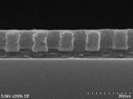
5 Process scheme of Self aligned DP Post Litho BARC trim SiO2 depo SiO2 Etch-back & core strip H/M Etch PR:80nm BARC:37nm Poly-Si:100nm 40nm hp 20nm hp 5

6 Pitch Quadrupling Litho 1 st HM etch Depo. Etch-back 2 nd HM etch Depo. Etch-back H/M Etch 45nm hp 23nm hp 11nm hp 23nm Pitch 6


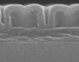
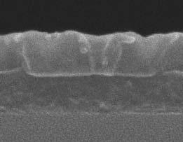
7 Spacer & Cut Process 40nm hp Photo-resist BARC 20nm hp Poly 20nm Core PR SADP Cut mask CD Shrink Final etch 40nm hp 20nm hp 20nm cut 7

 C.")
 K.")
8 2006/LELE Historical examination results V. Wiaux et al., imec IIAP (2006) C.bencher, et al., SPIE 7274 (2009) K. Oyama, et al., SPIE 7639 (2010) 8


 BARC&SiARC")


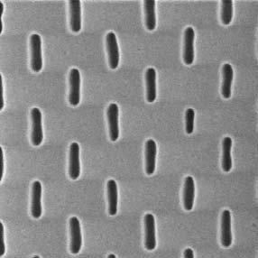
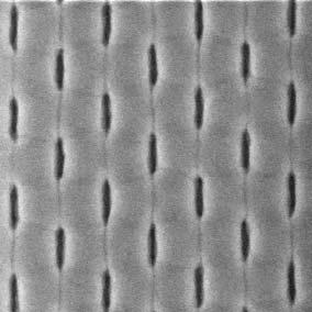
9 Spacer & Cut Process for trench pattern Core PR PR slimming Spacer Depo Spacer etchback 2nd PR (Bar) BARC&SiARC etch HM etch PR SiARC=30nm SOH=180nm SiN=50nm 48nm hp Dry slimming Etch back 24nm hp BARC 9


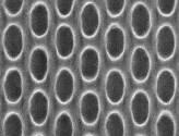
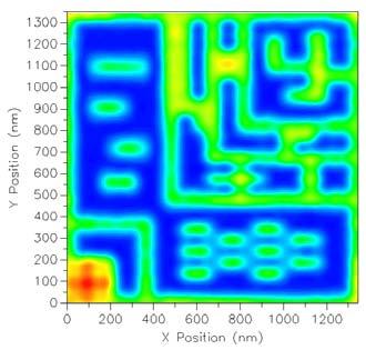
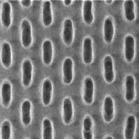
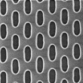
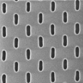
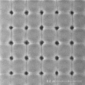
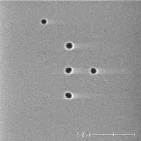
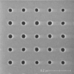
10 Spacer &Cut process for random layout post Litho. Pitch-doubling Cutting 50nm hp 25nm hp Random cut 10


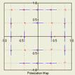
11 Image comparison Positive / negative tone resist Positive tone resist Mask Aerial image Negative tone resist Mask Aerial image (Bias+0/Serif+5) (Bias+5/Serif+10) Resist image Resist image 68.9nm 44.7nm NA1.3S0.98CP0.63 XYpolarized 6%attPSM 11


 Cut")
12 Resolution improvement Posi-type resist + ALD/SiO2 shrink Nega-type resist Cut mask PR (Posi resist) ALD SiO2 depo(6nm) Cut mask PR (Nega resist) 12

13 Image comparison Positive tone resist Negative tone resist 13


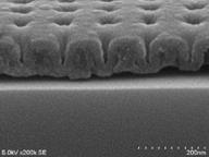
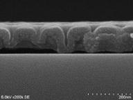
14 Short Summary ~ 193 Extension 193-i Resolution Limit Pitch-Doubling Pitch-Quadrupling 40nmhp 20nmhp 11nmhp Down scaling for gate 20nmhp for trench 24nmhp for Random 25nmhp Lay-out modification 14
15 Fundamental techniques for DP 15
16 CD bias control in DP schemes 1,LELE for line Trim Trim 2,LELE for trench/hole Shrink Shrink 3,LLE Trim Trim 4,Self-aligned DP Trim 16


17 Effective PR slimming control 1 Process time (a.u.) A/R=2.4 A/R=3.2 A/R=3.4 A/R=3.5 A/R=4.3 CD=39.8nm CD=28.0nm CD=25.0nm CD=22.8nm CD=18.1nm Height=94.2nm Height=89.2nm Height=84.1nm Height=79.3nm Height=78.4nm 17


18 Merit of CD bias control (Slimming) Dose control with Slimming Process window EL(%) DOF(um) 18


19 PR slimming for 2D pattern 19


20 Chemical assist Deposition Tapered Etching Hole shrink Schemes Litho. Chem. Apply Bake Litho. Film depo. Etch back Litho. Taper Etch Strip 20
")
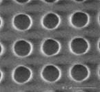
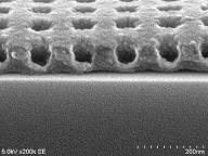
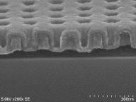
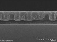
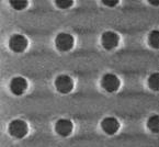
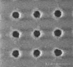
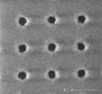
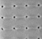
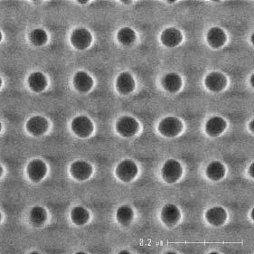
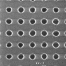
21 Control (0nm) Hole-shrink ~ SiO2 deposition SiO2 deposition thickness 5nm 10nm 15nm 25nm CD=65nm CD=55nm CD=45nm CD=35nm CD=15nm 21


")
![Thickness[A] 200.](/docs-images/76/73415003/images/22-5.jpg "0 150.0 100.0 50.0 0.")

22 CD bias control ~ ALD SiO2 Control : As Litho. Depo = 3nm Depo = 5nm Depo = 10nm Depo = 20nm Depo = 30nm y = x R 2 = Thickness (Å) Thickness[A] cycle# Process cycle# 22


23 Shrink property comparison control 20nm 25nm 30~35nm 40nm Chemical Assist Y=54.5nm X=118.8nm Y=34.4nm X=93.5nm Y=30.7nm X=81.3nm Y=25.3nm X=54.4nm SiO2 deposition Y=54.5nm X=118.8nm skip Y=30.1nm X=87.7nm Y=21.2nm X=79.7nm Y=14.5nm X=65.8nm 23
 140 120 100 80 60 40 20 X Y")

24 X-Y diameter linearity Hole size (nm) X Y : Chem. assist : SiO2 depo Shrink ammount (nm) 24

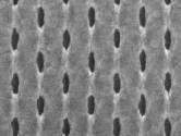
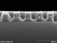
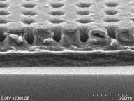
25 Pattern transfer reliability (1) Post-Litho. Hole shrink on TEOS Control w/o shrink Chemical Assist SiO2 Depo. 25

26 Pattern transfer reliability (2) Post-Litho. Hole shrink on TEOS Control w/o shrink Chemical Assist D=47.7nm SiO2 Depo. D=30.4nm 26
27 Summary H2O base immersion 193nm is still major exposure technique, and will be able to extend lithographic scaling combined with Double Patterning process SADP (Self-aligned spacer DP) can be modified easily to match well with restricted design rule. -SADP & Cut process for island, trench and complex 2D pattern Resist slimming is essential in any DP scheme to maintain wide process window. Hole shrink process with low-temp. SiO2 deposition can control the hole size precisely, and it may reduce the defect after etching. 27
28 Acknowledgement The author would like to express appreciation to Tokyo Electron / Leading-edge Process Development Center Tokyo Electron AT / Technical Development Center Tokyo Electron Kyushu / SPE process technology dept. Tokyo Electron Tohoku / Development dept. for their support in carrying out the experiments described in this paper. 28

29 Double Patterning Process TOKYO ELECTRON 29
Double patterning for 32nm and below: an update. Jo Finders, Mircea Dusa, Bert Vleeming, Birgitt Hepp, Henry Megens ASML
 Double patterning for 32nm and below: an update Jo Finders, Mircea Dusa, Bert Vleeming, Birgitt Hepp, Henry Megens ASML Mireille Maenhoudt, Shaunee Cheng, Tom Vandeweyer IMEC / Slide 1
Resist material for negative tone development process
 Resist material for negative tone development process FUJIFILM Corporation Electronic Materials Research Laboratories P-1 Outline 1. Advantages of negative tone imaging for DP 2. Process maturity of negative
Evolution of Optical Lithography towards 22nm and beyond Donis Flagello
 Evolution of Optical Lithography towards 22nm and beyond Donis Flagello Slide 1 ArF water immersion lithography cannot image 32 nm HP in SE 200 Resolution, Shrink (nm) 100 80 60 40 30 AT:1200 Logic NAND
Lithography Challenges Moore s Law Rising Costs and Challenges of Advanced Patterning
 Lithography Challenges Moore s Law Rising Costs and Challenges of Advanced Patterning SEMI Texas Spring Forum May 21, 2013 Austin, Texas Author / Company / Division / Rev. / Date A smartphone today has
Double patterning for 32nm and below: an update. ASML US Inc, 4211 Burton Dr. Santa Clara, CA, USA. IMEC vzw, Kapeldreef 75, B-3001 Heverlee, Belgium;
 Double patterning for 32nm and below: an update Jo Finders (a), Mircea Dusa (b) Bert Vleeming (a) Henry Megens (a) Birgitt Hepp (a) Mireille Maenhoudt (c), Shaunee Cheng (c), Tom Vandeweyer (c) (a) ASML,
Selective Processes: Challenges and Opportunities in Semiconductor Scaling
 Selective Processes: Challenges and Opportunities in Semiconductor Scaling June 4, 2018 Kandabara Tapily TEL Technology Center, America, LLC IITC 2018 Selective Deposition Workshop K. Tapily/ IITC 2018
FLCC Seminar. Spacer Lithography for Reduced Variability in MOSFET Performance
 1 Seminar Spacer Lithography for Reduced Variability in MOSFET Performance Prof. Tsu-Jae King Liu Electrical Engineering & Computer Sciences Dept. University of California at Berkeley Graduate Student:
Introduction to / Status of Directed Self- Assembly
 Introduction to / Status of Directed Self- Assembly DSA Workshop, Kobe Japan, October 2010 Bill Hinsberg IBM Almaden Research Center San Jose CA 95120 hnsbrg@almaden.ibm.com 2010 IBM Corporation from Bringing
4FNJDPOEVDUPS 'BCSJDBUJPO &UDI
 2010.5.4 1 Major Fabrication Steps in CMOS Process Flow UV light oxygen Silicon dioxide Silicon substrate Oxidation (Field oxide) photoresist Photoresist Coating Mask exposed photoresist Mask-Wafer Exposed
Figure 1 below shows the generic process flow of an LELE method of double patterning.
 Multilayer Double Patterning MCEE 505/605 LM&P Rajiv Sejpal (585) 622-8081 rns4256@rit.edu Dept. of Microelectronics Engineering, Rochester Institute of Technology GOAL Due to the delay in next generation
Litho scenario solutions for FinFET SRAM 22nm node
 See discussions, stats, and author profiles for this publication at: https://www.researchgate.net/publication/51695 Litho scenario solutions for FinFET SRAM nm node ARTICLE in PROCEEDINGS OF SPIE - THE
UHF-ECR Plasma Etching System for Dielectric Films of Next-generation Semiconductor Devices
 UHF-ECR Plasma Etching System for Dielectric Films of Next-generation Semiconductor Devices 1 UHF-ECR Plasma Etching System for Dielectric Films of Next-generation Semiconductor Devices Katsuya Watanabe
Patterning Challenges and Opportunities: Etch and Film
 Patterning Challenges and Opportunities: Etch and Film Ying Zhang, Shahid Rauf, Ajay Ahatnagar, David Chu, Amulya Athayde, and Terry Y. Lee Applied Materials, Inc. SEMICON, Taiwan 2016 Sept. 07-09, 2016,
SEMATECH Knowledge Series 2010
 SEMATECH Knowledge Series 2010 Summary of the SEMATECH Workshop on Directed Self Assembly Lloyd Litt SEMATECH/GF Bill Hinsberg - IBM 20 October 2010 Kobe, Japan Copyright 2010 Advanced Materials Research
Hyper-NA imaging of 45nm node random CH layouts using inverse lithography
 Hyper-NA imaging of 45nm node random CH layouts using inverse lithography E. Hendrickx* a, A. Tritchkov b, K. Sakajiri b, Y. Granik b, M. Kempsell c, G. Vandenberghe a a IMEC, Kapeldreef 75, B-3001, Leuven,
Developer-soluble Gap fill materials for patterning metal trenches in Via-first Dual Damascene process
 Developer-soluble Gap fill materials for patterning metal trenches in Via-first Dual Damascene process Mandar Bhave, Kevin Edwards, Carlton Washburn Brewer Science, Inc., 2401 Brewer Dr., Rolla, MO 65401,
Lithography and Etching
 Lithography and Etching Victor Ovchinnikov Chapters 8.1, 8.4, 9, 11 Previous lecture Microdevices Main processes: Thin film deposition Patterning (lithography) Doping Materials: Single crystal (monocrystal)
Photolithography Overview 9/29/03 Brainerd/photoclass/ECE580/Overvie w/overview
 http://www.intel.com/research/silicon/mooreslaw.htm 1 Moore s law only holds due to photolithography advancements in reducing linewidths 2 All processing to create electric components and circuits rely
Copyright 2000 by the Society of Photo-Optical Instrumentation Engineers.
 Copyright 2 by the Society of Photo-Optical Instrumentation Engineers. This paper was published in the proceedings of Photomask and X-Ray Mask Technology VII SPIE Vol. 466, pp. 172-179. It is made available
EE115C Winter 2017 Digital Electronic Circuits. Lecture 3: MOS RC Model, CMOS Manufacturing
 EE115C Winter 2017 Digital Electronic Circuits Lecture 3: MOS RC Model, CMOS Manufacturing Agenda MOS Transistor: RC Model (pp. 104-113) S R on D CMOS Manufacturing Process (pp. 36-46) S S C GS G G C GD
Optical Proximity Correction
 Optical Proximity Correction Mask Wafer *Auxiliary features added on mask 1 Overlay Errors + + alignment mask wafer + + photomask plate Alignment marks from previous masking level 2 (1) Thermal run-in/run-out
After Development Inspection (ADI) Studies of Photo Resist Defectivity of an Advanced Memory Device
 Studies of Photo Resist Defectivity of an Advanced Memory Device") After Development Inspection (ADI) Studies of Photo Resist Defectivity of an Advanced Memory Device Hyung-Seop Kim, Yong Min Cho, Byoung-Ho Lee Semiconductor R&D Center, Device Solution Business, Samsung
After Development Inspection (ADI) Studies of Photo Resist Defectivity of an Advanced Memory Device Hyung-Seop Kim, Yong Min Cho, Byoung-Ho Lee Semiconductor R&D Center, Device Solution Business, Samsung
EE141- Spring 2003 Lecture 3. Last Lecture
 - Spring 003 Lecture 3 IC Manufacturing 1 Last Lecture Design Metrics (part 1) Today Design metrics (wrap-up) IC manufacturing 1 Administrivia Discussion sessions start this week. Only one this week (Dejan
Top down and bottom up fabrication
 Lecture 24 Top down and bottom up fabrication Lithography ( lithos stone / graphein to write) City of words lithograph h (Vito Acconci, 1999) 1930 s lithography press Photolithography d 2( NA) NA=numerical
Plasma Etching: Atomic Scale Surface Fidelity and 2D Materials
 1 Plasma Etching: Atomic Scale Surface Fidelity and 2D Materials Thorsten Lill, Keren J. Kanarik, Samantha Tan, Meihua Shen, Alex Yoon, Eric Hudson, Yang Pan, Jeffrey Marks, Vahid Vahedi, Richard A. Gottscho
Fig The electron mobility for a-si and poly-si TFT.
 Fig. 1-1-1 The electron mobility for a-si and poly-si TFT. Fig. 1-1-2 The aperture ratio for a-si and poly-si TFT. 33 Fig. 1-2-1 All kinds defect well. (a) is the Dirac well. (b) is the repulsive Columbic
Technology Choices, Challenges and Timing Requirements for Nanolithography at the 32nm Node and Beyond
 Technology Choices, Challenges and Timing Requirements for Nanolithography at the 32nm Node and Beyond Christof Krautschik Technology & Manufacturing Group External Programs Intel, Santa Clara, CA October
Resist Materials Issues beyond 22 nm-hp Patterning for EUV Lithography
 Resist Materials Issues beyond 22 nm-hp Patterning for EUV Lithography February 26, 2009 Shinji Tarutani FUJIFILM Corporation Research & Development Management Headquarters Electronic Materials Research
nmos IC Design Report Module: EEE 112
 nmos IC Design Report Author: 1302509 Zhao Ruimin Module: EEE 112 Lecturer: Date: Dr.Zhao Ce Zhou June/5/2015 Abstract This lab intended to train the experimental skills of the layout designing of the
UNIVERSITY OF CALIFORNIA College of Engineering Department of Electrical Engineering and Computer Sciences. Fall Exam 1
 UNIVERSITY OF CALIFORNIA College of Engineering Department of Electrical Engineering and Computer Sciences EECS 143 Fall 2008 Exam 1 Professor Ali Javey Answer Key Name: SID: 1337 Closed book. One sheet
TEMPLATE AFFINITY ROLE IN CONTACT SHRINK BY DSA PLANARIZATION
 TEMPLATE AFFINITY ROLE IN CONTACT SHRINK BY DSA PLANARIZATION A. Gharbi, R. Tiron, M. Argoud, P. Pimenta Barros, S. Bos, G. Chamiotmaitral, I. Servin, A. Fouquet, J. Hazart (CEA-LETI) X. Chevalier, C.
Procédés de dépôt plasma avec injection pulsée de précurseurs (PECVD et PEALD) :
 :") Procédés de dépôt plasma avec injection pulsée de précurseurs (PECVD et PEALD) : Impact du réacteur et de la pression et développement de dépôts sélectifs C. Vallée 1,3, R. Gassilloud 2, R. Vallat 1,2,
Procédés de dépôt plasma avec injection pulsée de précurseurs (PECVD et PEALD) : Impact du réacteur et de la pression et développement de dépôts sélectifs C. Vallée 1,3, R. Gassilloud 2, R. Vallat 1,2,
There s Plenty of Room at the Bottom and at the Top
 14 nm chip X SEM from www.intel.com/content/dam/www/public/us/en/documents/pdf/foundry/mark bohr 2014 idf presentation.pdf There s Plenty of Room at the Bottom and at the Top Tsu Jae King Liu Department
Spectroscopic Critical Dimension technology (SCD) for Directed Self Assembly
 for Directed Self Assembly") Spectroscopic Critical Dimension technology (SCD) for Directed Self Assembly Senichi Nishibe a, Thaddeus Dziura a, Venkat Nagaswami a, Roel Gronheid b a KLA-Tencor Corporation, 1 Technology Drive, Milpitas
Spectroscopic Critical Dimension technology (SCD) for Directed Self Assembly Senichi Nishibe a, Thaddeus Dziura a, Venkat Nagaswami a, Roel Gronheid b a KLA-Tencor Corporation, 1 Technology Drive, Milpitas
Nanoimprint Lithography
 Nanoimprint Lithography Wei Wu Quantum Science Research Advanced Studies HP Labs, Hewlett-Packard Email: wei.wu@hp.com Outline Background Nanoimprint lithography Thermal based UV-based Applications based
Fiducial Marks for EUV mask blanks. Jan-Peter Urbach, James Folta, Cindy Larson, P.A. Kearney, and Thomas White
 Fiducial Marks for EUV mask blanks Jan-Peter Urbach, James Folta, Cindy Larson, P.A. Kearney, and Thomas White Fiducial marks are laser scribed on 200 mm wafers to enable defect registration on metrology
There's Plenty of Room at the Bottom
 There's Plenty of Room at the Bottom 12/29/1959 Feynman asked why not put the entire Encyclopedia Britannica (24 volumes) on a pin head (requires atomic scale recording). He proposed to use electron microscope
EE143 LAB. Professor N Cheung, U.C. Berkeley
 EE143 LAB 1 1 EE143 Equipment in Cory 218 2 Guidelines for Process Integration * A sequence of Additive and Subtractive steps with lateral patterning Processing Steps Si wafer Watch out for materials compatibility
Electron-beam SAFIER process and its application for magnetic thin-film heads
 Electron-beam SAFIER process and its application for magnetic thin-film heads XiaoMin Yang, a) Harold Gentile, Andrew Eckert, and Stanko R. Brankovic Seagate Research Center, 1251 Waterfront Place, Pittsburgh,
Ion Implantation. alternative to diffusion for the introduction of dopants essentially a physical process, rather than chemical advantages:
 Ion Implantation alternative to diffusion for the introduction of dopants essentially a physical process, rather than chemical advantages: mass separation allows wide varies of dopants dose control: diffusion
IC Fabrication Technology
 IC Fabrication Technology * History: 1958-59: J. Kilby, Texas Instruments and R. Noyce, Fairchild * Key Idea: batch fabrication of electronic circuits n entire circuit, say 10 7 transistors and 5 levels
Modeling Random Variability of 16nm Bulk FinFETs
 Modeling Random Variability of 16nm Bulk FinFETs Victor Moroz, Qiang Lu, and Munkang Choi September 9, 2010 1 Outline 2 Outline 3 16nm Bulk FinFETs for 16nm Node Simulation domain 24nm fin pitch 56nm gate
EUVL Readiness for High Volume Manufacturing
 EUVL Readiness for High Volume Manufacturing Britt Turkot Intel Corporation Outline Exposure Tool Progress Power Availability Intel demo results Reticle Defectivity Pellicle Materials Conclusion 2 Source
Development of Lift-off Photoresists with Unique Bottom Profile
 Transactions of The Japan Institute of Electronics Packaging Vol. 8, No. 1, 2015 [Technical Paper] Development of Lift-off Photoresists with Unique Bottom Profile Hirokazu Ito, Kouichi Hasegawa, Tomohiro
Gold Nanoparticles Floating Gate MISFET for Non-Volatile Memory Applications
 Gold Nanoparticles Floating Gate MISFET for Non-Volatile Memory Applications D. Tsoukalas, S. Kolliopoulou, P. Dimitrakis, P. Normand Institute of Microelectronics, NCSR Demokritos, Athens, Greece S. Paul,
Wet Chemical Processing with Megasonics Assist for the Removal of Bumping Process Photomasks
 Wet Chemical Processing with Megasonics Assist for the Removal of Bumping Process Photomasks Hongseong Sohn and John Tracy Akrion Systems 6330 Hedgewood Drive, Suite 150 Allentown, PA 18106, USA Abstract
ALD-enabled nanopatterning: area-selective ALD by area-activation
 ALD-enabled nanopatterning: area-selective ALD by area-activation Adrie Mackus, Ageeth Bol, and Erwin Kessels w.m.m.kessels@tue.nl www.tue.nl/pmp Outline Introduction & Area-selective deposition Area-selective
Extending the Era of Moore s Law
 14 nm chip X SEM from www.intel.com/content/dam/www/public/us/en/documents/pdf/foundry/mark bohr 2014 idf presentation.pdf Extending the Era of Moore s Law Tsu Jae King Liu Department of Electrical Engineering
EE 434 Lecture 12. Process Flow (wrap up) Device Modeling in Semiconductor Processes
 Device Modeling in Semiconductor Processes") EE 434 Lecture 12 Process Flow (wrap up) Device Modeling in Semiconductor Processes Quiz 6 How have process engineers configured a process to assure that the thickness of the gate oxide for the p-channel
EE 434 Lecture 12 Process Flow (wrap up) Device Modeling in Semiconductor Processes Quiz 6 How have process engineers configured a process to assure that the thickness of the gate oxide for the p-channel
Towards 3nm overlay and critical dimension uniformity: an integrated error budget for double patterning lithography
 Towards 3nm overlay and critical dimension uniformity: an integrated error budget for double patterning lithography Bill Arnold SPIE Advanced Lithography Optical SPIE 69-3 / Slide Outline Double patterning
Technologies VII. Alternative Lithographic PROCEEDINGS OF SPIE. Douglas J. Resnick Christopher Bencher. Sponsored by. Cosponsored by.
 PROCEEDINGS OF SPIE Alternative Lithographic Technologies VII Douglas J. Resnick Christopher Bencher Editors 23-26 February 2015 San Jose, California, United States Sponsored by SPIE Cosponsored by DNS
Sensors and Metrology. Outline
 Sensors and Metrology A Survey 1 Outline General Issues & the SIA Roadmap Post-Process Sensing (SEM/AFM, placement) In-Process (or potential in-process) Sensors temperature (pyrometry, thermocouples, acoustic
Carrier Transport by Diffusion
 Carrier Transport by Diffusion Holes diffuse ÒdownÓ the concentration gradient and carry a positive charge --> hole diffusion current has the opposite sign to the gradient in hole concentration dp/dx p(x)
ETCHING Chapter 10. Mask. Photoresist
 ETCHING Chapter 10 Mask Light Deposited Substrate Photoresist Etch mask deposition Photoresist application Exposure Development Etching Resist removal Etching of thin films and sometimes the silicon substrate
Cost Implications of EUV Lithography Technology Decisions
 Accelerating the next technology revolution Cost Implications of EUV Lithography Technology Decisions Andrea F. Wüest, SEMATECH Andrew J. Hazelton, Nikon Corporation Greg Hughes, SEMATECH Lloyd C. Litt,
Characteristics of Neutral Beam Generated by a Low Angle Reflection and Its Etch Characteristics by Halogen-Based Gases
 Characteristics of Neutral Beam Generated by a Low Angle Reflection and Its Etch Characteristics by Halogen-Based Gases Geun-Young Yeom SungKyunKwan University Problems of Current Etch Technology Scaling
More on Stochastics and the Phenomenon of Line-Edge Roughness
 More on Stochastics and the Phenomenon of Line-Edge Roughness Chris A. Mack 34 th International Photopolymer Science and Technology Conference Chiba, Japan, June 28, Conclusions We need more than just
Feature Profile Evolution during Shallow Trench Isolation (STI) Etch in Chlorine-based Plasmas
 Etch in Chlorine-based Plasmas") 1 Feature Profile Evolution during Shallow Trench Isolation (STI) Etch in Chlorine-based Plasmas Presentation November 14, 2005 Jane P. Chang and John Hoang Department of Chemical and Biomolecular Engineering
1 Feature Profile Evolution during Shallow Trench Isolation (STI) Etch in Chlorine-based Plasmas Presentation November 14, 2005 Jane P. Chang and John Hoang Department of Chemical and Biomolecular Engineering
Supplementary Figure 1 Detailed illustration on the fabrication process of templatestripped
 Supplementary Figure 1 Detailed illustration on the fabrication process of templatestripped gold substrate. (a) Spin coating of hydrogen silsesquioxane (HSQ) resist onto the silicon substrate with a thickness
Photomasks. Photolithography Evolution 9/11/2004 ECE580- MPE/MASKS/PHOTOMASKS.PPT
 Photolithography Evolution 1 : Evolution 2 Photomasks Substrates: Type : thermal expansion Chrome Pellicles Mask: OPC and PSM Fabrication: E-Beam or Laser 3 Photomask Information Websites: http://www.photronics.com/internet/corpcomm/publications/basics101/basics.
Recent progress in nanoparticle photoresist development for EUV lithography
 Recent progress in nanoparticle photoresist development for EUV lithography Kazuki Kasahara ab, Vasiliki Kosma b, Jeremy Odent b, Hong Xu b, Mufei Yu b, Emmanuel P. Giannelis b, Christopher K. Ober b a
Analysis of carbon contamination on EUV mask using CSM/ ICS
 Analysis of carbon contamination on EUV mask using CSM/ ICS Jae Uk Lee 1, Chang Young Jeong 1, Sangsul Lee 1, Jong Gul Doh 1,, Dong Geun Lee 2, Seong-Sue Kim 2, Han-Ku Cho 2, Seung-yu Rah 3 and Jinho Ahn
Pattern Transfer- photolithography
 Pattern Transfer- photolithography DUV : EUV : 13 nm 248 (KrF), 193 (ArF), 157 (F 2 )nm H line: 400 nm I line: 365 nm G line: 436 nm Wavelength (nm) High pressure Hg arc lamp emission Ref: Campbell: 7
Photolithography II ( Part 1 )
") 1 Photolithography II ( Part 1 ) Chapter 14 : Semiconductor Manufacturing Technology by M. Quirk & J. Serda Bjørn-Ove Fimland, Department of Electronics and Telecommunication, Norwegian University of Science
1 Photolithography II ( Part 1 ) Chapter 14 : Semiconductor Manufacturing Technology by M. Quirk & J. Serda Bjørn-Ove Fimland, Department of Electronics and Telecommunication, Norwegian University of Science
Cost of Ownership Considerations for Maskless Lithography
 Accelerating the next technology revolution Cost of Ownership Considerations for Maskless Lithography Lloyd C. Litt, SEMATECH Andrea F. Wüest, SEMATECH Copyright 2008 SEMATECH, Inc. SEMATECH, and the SEMATECH
Chapter 2. The Well. Cross Sections Patterning Design Rules Resistance PN Junction Diffusion Capacitance. Baker Ch. 2 The Well. Introduction to VLSI
 Chapter 2 The Well Cross Sections Patterning Design Rules Resistance PN Junction Diffusion Capacitance Joseph A. Elias, Ph.D. Adjunct Professor, University of Kentucky; Modeling MTS, Cypress Semiconductor
Across-wafer CD Uniformity Enhancement through Control of Multi-zone PEB Profiles
 Across-wafer CD Uniformity Enhancement through Control of Multi-zone PEB Profiles Qiaolin Zhang *a, Paul Friedberg b, Cherry Tang c Bhanwar Singh c, Kameshwar Poolla a, Costas J. Spanos b a Dept of Mechanical
J. Photopolym. Sci. Technol., Vol. 22, No. 5, Fig. 1. Orthogonal solvents to conventional process media.
 originates from the limited number of options regarding orthogonal solvents, i.e. solvents that do not dissolve or adversely damage a pre-deposited organic materials layer. The simplest strategy to achieve
High Optical Density Photomasks For Large Exposure Applications
 High Optical Density Photomasks For Large Exposure Applications Dan Schurz, Warren W. Flack, Makoto Nakamura Ultratech Stepper, Inc. San Jose, CA 95134 Microlithography applications such as advanced packaging,
The Impact of EUV on the Semiconductor Supply Chain. Scotten W. Jones President IC Knowledge LLC
 The Impact of EUV on the Semiconductor Supply Chain Scotten W. Jones President IC Knowledge LLC sjones@icknowledge.com Outline Why EUV Who needs EUV EUV adoption roadmaps EUV wafer volume projections Impact
Functional Materials for Advanced Patterning Robert D. Allen. IBM Almaden Research Center
 Functional Materials for Advanced Patterning Robert D. Allen Business Unit or Product Name IBM Almaden Research Center 2003 IBM Corporation Resists/Materials for Advanced Patterning Trends in Lithography
Dry Etching Zheng Yang ERF 3017, MW 5:15-6:00 pm
 Dry Etching Zheng Yang ERF 3017, email: yangzhen@uic.edu, MW 5:15-6:00 pm Page 1 Page 2 Dry Etching Why dry etching? - WE is limited to pattern sizes above 3mm - WE is isotropic causing underetching -
Chapter 2. Design and Fabrication of VLSI Devices
 Chapter 2 Design and Fabrication of VLSI Devices Jason Cong 1 Design and Fabrication of VLSI Devices Objectives: To study the materials used in fabrication of VLSI devices. To study the structure of devices
Tilted ion implantation as a cost-efficient sublithographic
 Tilted ion implantation as a cost-efficient sublithographic patterning technique Sang Wan Kim 1,a), Peng Zheng 1, Kimihiko Kato 1, Leonard Rubin 2, Tsu-Jae King Liu 1 1 Department of Electrical Engineering
Chapter 3 : ULSI Manufacturing Technology - (c) Photolithography
 Photolithography") Chapter 3 : ULSI Manufacturing Technology - (c) Photolithography 1 Reference 1. Semiconductor Manufacturing Technology : Michael Quirk and Julian Serda (2001) 2. - (2004) 3. Semiconductor Physics and Devices-
Chapter 3 : ULSI Manufacturing Technology - (c) Photolithography 1 Reference 1. Semiconductor Manufacturing Technology : Michael Quirk and Julian Serda (2001) 2. - (2004) 3. Semiconductor Physics and Devices-
Critical Dimension Uniformity using Reticle Inspection Tool
 Critical Dimension Uniformity using Reticle Inspection Tool b Mark Wylie, b Trent Hutchinson, b Gang Pan, b Thomas Vavul, b John Miller, b Aditya Dayal, b Carl Hess a Mike Green, a Shad Hedges, a Dan Chalom,
UNIT 3. By: Ajay Kumar Gautam Asst. Prof. Dev Bhoomi Institute of Technology & Engineering, Dehradun
 UNIT 3 By: Ajay Kumar Gautam Asst. Prof. Dev Bhoomi Institute of Technology & Engineering, Dehradun 1 Syllabus Lithography: photolithography and pattern transfer, Optical and non optical lithography, electron,
Lecture 150 Basic IC Processes (10/10/01) Page ECE Analog Integrated Circuits and Systems P.E. Allen
 Page ECE Analog Integrated Circuits and Systems P.E. Allen") Lecture 150 Basic IC Processes (10/10/01) Page 1501 LECTURE 150 BASIC IC PROCESSES (READING: TextSec. 2.2) INTRODUCTION Objective The objective of this presentation is: 1.) Introduce the fabrication of
Lecture 150 Basic IC Processes (10/10/01) Page 1501 LECTURE 150 BASIC IC PROCESSES (READING: TextSec. 2.2) INTRODUCTION Objective The objective of this presentation is: 1.) Introduce the fabrication of
EE C245 ME C218 Introduction to MEMS Design Fall 2007
 EE C245 ME C218 Introduction to MEMS Design Fall 2007 Prof. Clark T.-C. Nguyen Dept. of Electrical Engineering & Computer Sciences University of California at Berkeley Berkeley, CA 94720 Lecture 5: ALD,
Accurate and Reliable Optical CD of MuGFET down to 10nm
 Accurate and Reliable Optical D of MuGFET down to 1nm P Leray 1, G F Lorusso 1, heng 1, N ollaert 1, M Jurczak 1, hirke 2 1 IME, Kapeldreef 75, B31, Leuven, Belgium 2 VLI tandard, 387 N 1st treet an Jose
MICROCHIP MANUFACTURING by S. Wolf
 by S. Wolf Chapter 15 ALUMINUM THIN-FILMS and SPUTTER-DEPOSITION 2004 by LATTICE PRESS CHAPTER 15 - CONTENTS Aluminum Thin-Films Sputter-Deposition Process Steps Physics of Sputter-Deposition Magnetron-Sputtering
DO NOT WRITE YOUR NAME OR KAUST ID NUMBER ON THIS PAGE OR ANY OTHER PAGE PUT YOUR EXAM ID NUMBER ON THIS PAGE AND EVERY OTHER PAGE YOU SUBMIT
 DO NOT WRITE YOUR NAME OR KAUST ID NUMBER ON THIS PAGE OR ANY OTHER PAGE PUT YOUR EXAM ID NUMBER ON THIS PAGE AND EVERY OTHER PAGE YOU SUBMIT WRITE YOUR SOLUTIONS ON ONLY ONE SIDE OF EMPTY SOLUTION SHEETS
Methodology of modeling and simulating line-end shortening effects in deep-uv resist
 Methodology of modeling and simulating line-end shortening effects in deep-uv resist Mosong Cheng*, Ebo Croffie, Andrew Neureuther Electronics Research Laboratory Department of Electrical Engineering and
Simulation and characterization of surface and line edge roughness in photoresists before and after etching
 Simulation and characterization of surface and line edge roughness in photoresists before and after etching Motivation of this work : Sub 100nm lithographic features often suffer from roughness. Need to
Self-study problems and questions Processing and Device Technology, FFF110/FYSD13
 Self-study problems and questions Processing and Device Technology, FFF110/FYSD13 Version 2016_01 In addition to the problems discussed at the seminars and at the lectures, you can use this set of problems
Automatic Classification and Defect Verification Based on Inspection Technology with Lithography Simulation
 Automatic Classification and Defect Verification Based on Inspection Technology with Lithography Simulation Masaya Kato a, Hideki Inuzuka a, Takeshi Kosuge a, Shingo Yoshikawa a, Koichi Kanno a, Hidemichi
MEEN Nanoscale Issues in Manufacturing. Lithography Lecture 1: The Lithographic Process
 MEEN 489-500 Nanoscale Issues in Manufacturing Lithography Lecture 1: The Lithographic Process 1 Discuss Reading Assignment 1 1 Introducing Nano 2 2 Size Matters 3 3 Interlude One-The Fundamental Science
Novel Approach of Semiconductor BEOL Processes Integration
 Novel Approach of Semiconductor BEOL Processes Integration Chun-Jen Weng cjweng825@yahoo.com.tw Proceedings of the XIth International Congress and Exposition June 2-5, 2008 Orlando, Florida USA 2008 Society
Techniken der Oberflächenphysik (Techniques of Surface Physics)
") Techniken der Oberflächenphysik (Techniques of Surface Physics) Prof. Yong Lei & Dr. Yang Xu (& Liying Liang) Fachgebiet 3D-Nanostrukturierung, Institut für Physik Contact: yong.lei@tu-ilmenau.de; yang.xu@tu-ilmenau.de;
Techniken der Oberflächenphysik (Techniques of Surface Physics) Prof. Yong Lei & Dr. Yang Xu (& Liying Liang) Fachgebiet 3D-Nanostrukturierung, Institut für Physik Contact: yong.lei@tu-ilmenau.de; yang.xu@tu-ilmenau.de;
Electrical and Reliability Characteristics of RRAM for Cross-point Memory Applications. Hyunsang Hwang
 Electrical and Reliability Characteristics of RRAM for Cross-point Memory Applications Hyunsang Hwang Dept. of Materials Science and Engineering Gwangju Institute of Science and Technology (GIST), KOREA
Chapter 3 Basics Semiconductor Devices and Processing
 Chapter 3 Basics Semiconductor Devices and Processing Hong Xiao, Ph. D. www2.austin.cc.tx.us/hongxiao/book.htm Hong Xiao, Ph. D. www2.austin.cc.tx.us/hongxiao/book.htm 1 Objectives Identify at least two
CHAPTER 6: Etching. Chapter 6 1
 Chapter 6 1 CHAPTER 6: Etching Different etching processes are selected depending upon the particular material to be removed. As shown in Figure 6.1, wet chemical processes result in isotropic etching
Thin Wafer Handling Debonding Mechanisms
 Thin Wafer Handling Debonding Mechanisms Jonathan Jeauneau, Applications Manager Alvin Lee, Technology Strategist Dongshun Bai, Scientist, 3-D IC R&D Materials Outline Requirements of Thin Wafer Handling
A Novel Approach to the Layer Number-Controlled and Grain Size- Controlled Growth of High Quality Graphene for Nanoelectronics
 Supporting Information A Novel Approach to the Layer Number-Controlled and Grain Size- Controlled Growth of High Quality Graphene for Nanoelectronics Tej B. Limbu 1,2, Jean C. Hernández 3, Frank Mendoza
Introduction. Photoresist : Type: Structure:
 Photoresist SEM images of the morphologies of meso structures and nanopatterns on (a) a positively nanopatterned silicon mold, and (b) a negatively nanopatterned silicon mold. Introduction Photoresist
Mask Characterization for Double Patterning Lithography
 Mask Characterization for Double Patterning Lithography Karsten Bubke 1, Eric Cotte 1, Jan Hendrik Peters 1, Robert de Kruif, Mircea Dusa 3, Joerg Fochler 4, Brid Connolly 4 1 Advanced Mask Technology
Development of Photosensitive Polyimides for LCD with High Aperture Ratio. May 24, 2004
 Development of Photosensitive Polyimides for LCD with High Aperture Ratio May 24, 2004 utline Why is polymer dielectric required for TFT LCD? Requirements of the polymer dielectrics What is polyimide?
Objective: Competitive Low-Cost Thin-Film Varactor Technology. Integrated Monolithic Capacitors using Sputtered/MOCVD material on low-cost substrates
 Overview of Program Objective: Competitive Low-Cost Thin-Film Varactor Technology coplanar waveguide (CPW) capacitor ground signal ground Si substrate etched troughs Focus of Our Program! Reproducibility!
Taurus-Topography. Topography Modeling for IC Technology
 SYSTEMS PRODUCTS LOGICAL PRODUCTS PHYSICAL IMPLEMENTATION SIMULATION AND ANALYSIS LIBRARIES TCAD Aurora DFM WorkBench Davinci Medici Raphael Raphael-NES Silicon Early Access TSUPREM-4 Taurus-Device Taurus-Lithography
ELEN0037 Microelectronic IC Design. Prof. Dr. Michael Kraft
 ELEN0037 Microelectronic IC Design Prof. Dr. Michael Kraft Lecture 2: Technological Aspects Technology Passive components Active components CMOS Process Basic Layout Scaling CMOS Technology Integrated