Plastic Deformations in Mechanically Strained Single-Walled Carbon Nanotubes. Department of Physics, Harvard University, Cambridge, MA 02138
|
|
|
- Dinah Harrington
- 5 years ago
- Views:
Transcription
1 Plastic Deformations in Mechanically Strained Single-Walled Carbon Nanotubes Dolores Bozovic*, M. Bockrath Department of Physics, Harvard University, Cambridge, MA Jason H. Hafner, Charles M. Lieber, Hongkun Park Department of Chemistry and Chemical Biology, Harvard University, Cambridge, MA M. Tinkham Department of Physics, Harvard University, Cambridge, MA *present address: Rockefeller University, New York, NY Abstract AFM manipulation was used to controllably stretch individual metallic singlewalled carbon nanotubes (SWNTs). We have found that SWNTs can sustain elongations as great as 30% without breaking. Scanned gate microscopy and transport measurements were used to probe the effects of the mechanical strain on the SWNT electronic properties, which revealed a strain-induced increase in intra-tube electronic scattering above a threshold strain of ~5-10%. These findings are consistent with theoretical calculations predicting the onset of plastic deformation and defect formation in carbon nanotubes. 1
2 Due to their extraordinary mechanical and electronic properties and potential applications in molecular electronics, single-walled carbon nanotubes (SWNTs) have been the focus of much attention during the past ten years 1,2. SWNTs provide experimental realizations of quasi-one-dimensional conductors, which can be either metallic or semiconducting depending on their radii and chiralities. Although early studies focused on defect-free metallic nanotubes 3-5, several recent experiments have explored the effects of intrinsic structural defects on the electronic properties of SWNTs 6-8. These defects have also been directly revealed in atomic-resolution scanning tunneling microscope imaging experiments 6, studied using electron transport measurements and scanned gate microscopy 9, and shown to act as resonant scattering centers 7. In addition, Park et al. 10 have demonstrated that new defects can be induced via ion implantation and examined their effects on transport. The effects of mechanical distortion on nanotube transport have also been the subject of both theoretical and experimental study. Tombler et al. used an AFM tip to produce small-angle reversible bending and elongation in nanotubes, while measuring the nanotube conduction 11,12. A number of groups have also performed calculations to theoretically study the effects of large distortions and mechanical strain, the formation of new defects in nanotubes 13-19, and their effects on transport properties In particular, the effect of axial elongation on the mechanical and electronic structure of carbon nanotubes has been the subject of extensive theoretical study. Calculations using tightbinding and local density approximation methods have predicted that tubes should elongate elastically up to a critical strain that depends on the radius and chirality of the tube. For larger strains, introduction of topological defects, such as bond-rotations, 2
3 becomes energetically favorable According to calculations by Zhang et al. 13, critical elongations fall in the range of 6% (armchair) to 12% (zigzag) for nanotubes with diameters of ~1 nm. Further study of defect formation is motivated by the importance of their role in the electron transport properties of carbon nanotubes. Previous experimental studies of mechanically induced structural defects have been performed on MWNTs 23 and ropes of SWNTs 24. Here, we present experimental observations of the effects of mechanical strain on the electronic properties of individual SWNTs. We used an atomic force microscope (AFM) tip to locally move nanotubes 11,25,26 along a SiO 2 substrate and elongate them in a controlled fashion. Using the technique of scanned gate microscopy (SGM) 9,27, we studied scattering by intra-tube defects both before and after manipulation. By varying the extent of the strain, we detected increases in electron back-scattering induced by localized longitudinal strain when the strain exceeded a characteristic value of ~5-10%, in agreement with the theoretically predicted range of threshold strains. The substrates used in these experiments were degenerately doped silicon wafers with 1 µm of SiO 2 on top. We studied single-walled carbon nanotubes synthesized by two different methods. Nanotubes grown by the laser arc-discharge technique 28 were dispersed in ethylene dichloride by ultrasonic agitation and deposited onto the silicon substrates. In order to select for single nanotubes, we imaged the samples with tappingmode AFM and selected only tubes ~1 nm in height. Individual SWNTs synthesized by the chemical vapor deposition method 29,30 were grown directly onto the surface of the silicon wafers. 3
4 The nanotube samples were imaged in tapping mode with a Digital Instruments AFM, and the nanotubes positions were determined relative to a pre-defined grid of markers. After spin-casting a suitable resist bi-layer, we used electron-beam lithography to pattern the positions of electrodes on top of the nanotubes. A 50 Å adhesion layer of Cr and a 450 Å layer of Au was thermally evaporated onto the substrates to form the electrodes. The remaining resist was removed by immersion in acetone. An AFM image of one such device is shown in Fig. 1(a). Devices incorporating metallic SWNTs were then selected, based on the behavior of their conductance vs. the voltage V g applied to the substrate, which acts as a gate electrode 1-5. Pushing on the nanotube segment between the leads with an AFM tip 25,26,31 induces mechanical strain in the tube. Before AFM manipulation, we first imaged the tubes in tapping mode. We then set the oscillation amplitude of the tip to zero and disengaged the scanner feedback. Lowering the tip further by ~100 nm brings it into contact with the substrate surface nearby the nanotube. In this state, moving the tip laterally pushes the nanotube along with it. Figs. 1 (a) and (b) show tapping-mode images of a nanotube before and after pushing it in a direction perpendicular to its long axis. Varying the extent of the lateral tip motion produces controllable levels of axial strain in the carbon nanotube. Imaging the nanotube after such deformation (see Fig. 1(b)) reveals that frictional forces between the tube and the substrate are sufficient to maintain the elongation of the SWNTs after the removal of the AFM tip. Comparing the topographic images taken before and after straining (left panels of Fig. 2 (a) and (b)), we observed that neither the shape nor the position of the nanotubes is visibly altered by manipulation except near where the AFM tip pushed the nanotube. This 4
5 indicates that the displacement-induced strain is non-uniform. To obtain an approximate estimate of the local average strain within the observably displaced region, we make two simplifying assumptions: that most of the strain is localized to the region that visibly moved under manipulation, and that it is uniformly distributed within this region. We measure the average strain by comparing the lengths of the SWNT segments that moved visibly before and after straining. The location of these perturbed segments was determined by overlaying the topographic images taken before and after straining, and their respective lengths were digitally measured using a standard drawing software package [Deneba Canvas 5.0]. We found that local average elongations as great as 30% could be achieved without breaking the nanotubes mechanically or electrically, allowing us to study strains well into the theoretically predicted plastic regime. Outside of the maximally strained region, we estimate the typical strain to be 1%, based on the positional measurement resolution in our experiment of ~20 nm. Several checks were performed to verify that the tubes were indeed elongated in the central segment between the metallic electrodes, rather than sliding along the surface axially. We took topographic AFM images of nanotube devices before and after AFM manipulation, directly comparing the positions of the tube ends. In over 30 samples that we strained in this fashion, we have never observed any sliding in of the nanotube ends. Another possible mechanism of strain release would be nanotubes breaking and sliding directly underneath the gold electrodes. As a check, we strained a number of nanotube samples sufficiently that, had the ends been broken, they would have been pulled out entirely from beneath the leads. This was not observed in any of the samples. Furthermore, we found that nanotubes do eventually break under sufficient strain, but we 5
6 have always found them to break close to the point where they were pushed by the tip, indicating that, for large tip displacements, the strain is concentrated near the point of manipulation. To determine whether the elongation altered the electronic properties of the SWNTs, the SWNTs were probed both before and after manipulation using scanned gate microscopy 9,27 (SGM) and transport measurements. In SGM, a voltage is applied to a conductive AFM tip (typically in our experiment 5-10 V), which is used as a moveable gate. Bringing the tip to a position directly above a nanotube modulates the local charge density in the tube and therefore shifts its local Fermi level. Moving the tip further away decreases its capacitive coupling to the nanotube and therefore reduces its gating effect. Plotting the conductance of the tube as a function of the tip position for fixed V g yields a spatially resolved image of the effects of this modulation. In our previous work 7, we studied scattering of electrons by intrinsic defects in single-walled carbon nanotubes. As-grown metallic tubes were found to exhibit conductances with non-monotonic dependence on V g. SGM images that were taken on these devices showed ring-like features, which were interpreted as signatures of resonant scattering by intrinsic defects. According to theoretical predictions 20, these defects (for example, vacancies) lead to quasi-bound defect states, which in turn give rise to increased scattering at specific energies. Both types of nanotubes used in this experiment, those grown by the laser arc-discharge and those grown by the chemical vapor deposition methods, were found to contain a number of native defects. Following this measurement on unstrained nanotubes, we used AFM manipulation to induce varying degrees of strain in SWNTs, in the range of ~2-30%, and 6
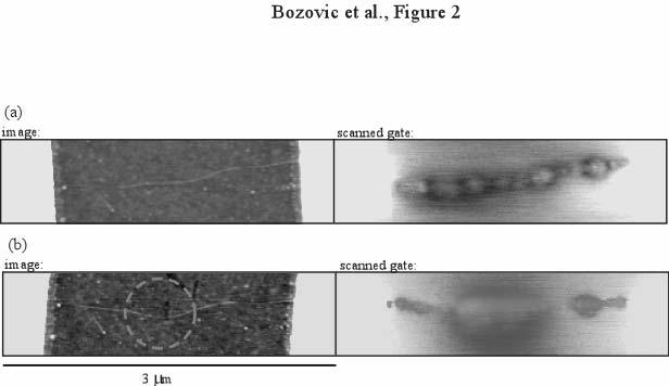
7 investigated the resulting impact on the nanotube electronic properties. In devices strained by only a few percent, we did not observe the introduction of new scattering centers in the SGM scans. This indicates that mere contact with the AFM tip is not sufficient to introduce new scattering centers in the nanotube lattice, and hence, the tube elongation is most likely elastic. For larger strains, we observed qualitatively different behavior. Figure 2 shows topographic and scanned gate images taken on a nanotube device before and after AFM manipulation, where a change in electronic properties occurred. A local elongation of ~7 ± 1% over a length of about 520 nm was induced in this nanotube. The scanned gate image taken before straining showed a number of intrinsic defects. After manipulation, the SGM image corresponding to the maximally strained portion (characterized by having observable displacement) of the nanotube shows one large feature. The SGM image corresponding to the remaining portion of the tube, on the contrary, still shows relatively smaller features corresponding to individual scattering centers. These are qualitatively similar in appearance to ones shown in Fig. 2(a), although the individual scatterers show increased resistances as compared to the unstrained tube. Thus we find that the perturbation caused by the tip affects transport properties of the SWNT differently, depending on whether it was scanned over the maximally strained or the remaining segments respectively. This also indicates that the AFM manipulation modulates the electronic properties of the SWNT along the entire observably displaced region. The resistance of this sample as a function of V g is shown in Fig. 3. The plots show V g sweeps taken before and after deformation of the nanotube. Both scans show 7
8 gate modulation characteristic of tubes with defects 7, consistent with the appearance of rings in the corresponding before and after SG images, with a peak in the resistance occurring at positive V g. As can be seen from these two scans, the resistance of the nanotube for V g where the defects scatter most strongly (maximum in the resistance rise) has increased by a factor of ~20 after the induced elongation. On the other hand, when V g is tuned away from the maximum resistance value (negative V g ) the resistance had changed only by a small amount. The large increase in the nanotube resistance occurring selectively at particular values of V g, together with the local change in electronic properties of the strained SWNT segment evinced by the SGM images, shows that the maximally strained SWNT portion shows an increase in back-scattering that is resonant in nature. Overall, for samples strained above 10%, comparing the resistances and SGM images taken before and after straining revealed similar behavior to the sample shown above. In the intermediate regime, from ~5-10% strain, some samples showed an increase in local back-scattering, while others did not. Samples elongated less than 5% showed little change in behavior. Theoretical calculations predict that the critical strains for defect formation depend on nanotube chiralities 13, falling in the range from 6 to 12%. Although we do not know the detailed atomic structure of our nanotubes, we have induced a wide range of elongations, and observed dramatic increases in local back-scattering for strains higher than ~5-10%, which is consistent with these theoretical predictions for the onset of plastic deformation and defect formation. For each of our samples, we also measured the nanotube diameters from the topographic AFM scans. We observed no notable dependence of the electronic scattering properties on diameter in the measured range of 8
9 ~1-3 nm. Finally, we note that the changes evident in the SGM images corresponding to the portions of the SWNT outside the maximally strained region may result from the distortion of intrinsic defects, causing them to scatter more strongly. Further theoretical and experimental work is required to fully characterize and understand this effect. In conclusion, we have used an atomic force microscope tip to induce varying degrees of strain in single-walled carbon nanotubes. Due to the robustness of the nanotube lattice, strains as great as 30% can be reproducibly induced, bringing the nanotube into the theoretically anticipated regime of plastic deformation. Transport measurements and scanned gate microscopy were then used to study scattering in nanotubes before and after manipulation and to thereby observe the induced increase in local resonant back-scattering. Elucidation of the threshold of defect formation in nanotubes, besides providing insight into their structure, is an important step towards their potential applications as strengthening materials and as miniature electromechanical devices. This research was supported in part by NSF grants DMR and PHY
10 References 1 C. Dekker, Physics Today 52, 22 (1999). 2 P. L. McEuen, Physics World 13, 31 (2000). 3 S. J. Tans, M. H. Devoret, H. Dai, A. Thess, R. E. Smalley, L. J. Georliga, and C. Dekker, Nature 386, 474 (1997). 4 M. Bockrath, D. H. Cobden, P. L. McEuen, N. G. Chopra, A. Zettl, A. Thess, and R. E. Smalley, Science 275, 1922 (1997). 5 T. W. Odom, J.-L. Huang, P. Kim, and C. M. Lieber, Nature 391, 62 (1998). 6 M. Ouyang, J.-L. Huang, C. L. Cheung, and C. M. Lieber, Science 291, 98 (2001). 7 M. Bockrath, W. Liang, D. Bozovic, J. H. Hafner, C. M. Lieber, M. Tinkham, and H. Park, Science 291, 283 (2000). 8 Z. Yao, H. W. C. Postma, L. Balents, and C. Dekker, Nature 402, 273 (1999). 9 A. Bachtold, M. Fuhrer, S. Plyasunov, M. Forero, E. H. Anderson, A. Zettl, and P. L. McEuen, Phys. Rev. Lett. 84, 6082 (2000). 10 J. W. Park, Jinhee Kim, J.-O. Lee, K. C. Kang, J.-J. Kim, and K.-H. Yoo, Appl. Phys. Lett 80, 133 (2002). 11 T. W. Tombler, C. W. Zhou, L. Alexseyev, J. Kong, H. J. Dai, L. Lei, C. S. Jayanthi, M. J. Tang, and S. Y. Wu, Nature 405, 769 (2000). 12 L. Liu, C. X. Jayanthi, M. Tang, S. Y. Wu, T. W. Tombler, C. Zhou, L. Alexseyev, J. Kong, and H. Dai, Phys. Rev. Lett. 84, 4950 (2000). 13 P. Zhang, P. E. Lammert, and V. H. Crespi, Phys. Rev. Lett. 81, 5346 (1998). 14 B. V. Pan, W. S. Yang, and J. Yang, Phys. Rev. B 62, (2000). 15 B. I. Yakobson, Appl. Phys. Lett, 72, 918 (1998). 10
11 16 M. B. Nardelli, B. I. Yakobson, and J. Bernholc, Phys. Rev. B 57, 4277 (1998). 17 M. B. Nardelli, B. I. Yakobson, and J. Bernholc, Phys. Rev. Lett. 81, 4656 (1998). 18 M. B. Nardelli and J. Bernholc, Phys. Rev. B 60, R16338 (1999). 19 A. Rochefort, P. Avouris, F. Lesage, and D. R. Salahub, Phys. Rev. B 60, (1999). 20 H. J. Choi, J. Ihm, S. G. Louie, and M. l. Cohen, Phys. Rev. Lett. 84, 2917 (2000). 21 J. C. Charlier, T. W. Ebbesen, and P. Lambin, Phys. Rev. B 53, (1996). 22 P. L. McEuen, M. Bockrath, D. H. Cobden, Y.-G. Yoon, and S. G. Louie, Phys. Rev. Lett. 83, 5098 (1999). 23 S. Paulson, M. R. Falvo, N. Snider, A. Helser, T. Hudson, A. Seeger, R. M. Taylor, R. Superfine, and S. Washburn, Appl. Phys. Lett. 75, 2936 (1999). 24 D. A. Walters, L. M. Ericson, M. J. Casavant, J. Liu, D. T. Colbert, K. A. Smith, and R. E. Smalley, Appl. Phys. Lett. 74, 3803 (1999). 25 T. Hertel, R. Martel, and P. Avouris, J. of Phys. Chem. B 102, 910 (1998). 26 P. Avouris, T. Hertel, R. Martel, T. Schmidt, H. R. Shea, and R. E. Walkup, App. Surf. Sci. 141, 201 (1999). 27 S. J. Tans and C. Dekker, Nature 404, 834 (2000). 28 A. Thess, R. Lee, P. Nikolaev, H. Dai, P. Petit, J. Robert, C. Xu, Y. H. Lee, S. G. Kim, A. G. Rinzler, D. T. Colbert, G. E. Scuseria, D. Tombnek, J. E. Fischer, and R. E. Smalley, Science 273, 483 (1996). 29 J. H. Hafner, M. J. Bronikowski, B. R. Azamian, P. Nikolaev, A. G. Rinzler, D. T. Colbert, K. A. Smith, and R. E. Smalley, Chem. Phys. Lett. 296, 195 (1998). 30 J. H. Hafner, C. L. Cheung, and C. M. Lieber, J. of Amer. Chem. Soc. 121, 9750 (1999). 11
12 31 J. Lefebvre, J.F. Lynch, M. Llaguno, M. Radosavljevic, and A.T. Johnson, Appl. Phys. Lett. 75, 3014 (1999). 12
13 Figure captions FIG. 1. Differential tapping-mode AFM color-enhanced images were taken (a) before and (b) after straining the nanotube with the AFM tip. In this device, Cr/Au leads had been deposited on top of the SWNT (the underlying tube formed small ridges in the surface of the metallic leads). As the nanotubes were anchored to the surface by the gold electrodes, this manipulation forced the central portion of the tube to elongate. FIG 2. (a) The top panel gives topographic (left) and SGM (right) images taken on a nanotube device before AFM manipulation. The data scale in this SGM image has been adjusted to correspond to a range from µs, darkest to lightest areas respectively. (b) The bottom panel shows images taken on the same device after straining. The data scale in this image ranges from 0.2 to 15 µs. We used two different conductive tips to acquire these two images, with a tip voltage of 10V applied to both. FIG 3. Resistance is plotted as a function of the V g, measured on the device shown in Figure 2. The curves show scans measured (a) before and (b) after straining the nanotube. Please note the difference in scales between the two plots. The peaks in the resistance correspond to maximal scattering by the induced scattering centers, as tuned by varying V g. The graphs indicate that the nanotube resistance had not changed significantly in absolute amount in the region of negative V g, whereas it had increased by a factor of ~20 in the regimes where the centers have been tuned to scatter maximally. Both measurements were taken at room temperature. 13
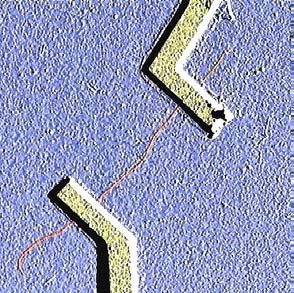
14 Bozovicetal.,Figure1 (a) (b) 5 m AFM tip 14
15 15
16 Bozovic et al., Figure 3 R (kω) R (kω) (a) V g (V) (b) V g (V) 16
Atomically Resolved Single-Walled Carbon Nanotube Intramolecular Junctions
 Atomically Resolved Single-Walled Carbon Nanotube Intramolecular Junctions The Harvard community has made this article openly available. Please share how this access benefits you. Your story matters Citation
Electronic transport through bent carbon nanotubes: Nanoelectromechanical sensors and switches
 Electronic transport through bent carbon nanotubes: Nanoelectromechanical sensors and switches Amir A. Farajian, 1, * Boris I. Yakobson, 2 Hiroshi Mizuseki, 1 and Yoshiyuki Kawazoe 1 1 Institute for Materials
Effects of Defects on the Strength of Nanotubes: Experimental- Computational Comparisons
 Effects of Defects on the Strength of Nanotubes: Experimental- Computational Comparisons T. Belytschko, S. P. Xiao and R. Ruoff Department of Mechanical Engineering Northwestern University, 2145 Sheridan
SINGLE-ELECTRON DETECTION AND MEMORY USING A SINGLE CARBON NANOTUBE DEFECT
 SINGLE-ELECTRON DETECTION AND MEMORY USING A SINGLE CARBON NANOTUBE DEFECT B. M. Kim, Yung-Fu Chen and M. S. Fuhrer * Department of Physics, University of Maryland, College Park, MD 20742-4111 A single
Effect of strain on the band gap and effective mass of zigzag single-wall carbon nanotubes: First-principles density-functional calculations
 PHYSICAL REVIEW B 77, 1553 8 Effect of strain on the band gap and effective mass of zigzag single-wall carbon nanotubes: First-principles density-functional calculations S. Sreekala, 1, * X.-H. Peng, 1
Electric Field-Dependent Charge-Carrier Velocity in Semiconducting Carbon. Nanotubes. Yung-Fu Chen and M. S. Fuhrer
 Electric Field-Dependent Charge-Carrier Velocity in Semiconducting Carbon Nanotubes Yung-Fu Chen and M. S. Fuhrer Department of Physics and Center for Superconductivity Research, University of Maryland,
Local buckling of carbon nanotubes under bending
 APPLIED PHYSICS LETTERS 91, 093128 2007 Local buckling of carbon nanotubes under bending Q. Wang a Department of Mechanical and Manufacturing Engineering, University of Manitoba, Winnipeg, Manitoba R3T
7.0 nm. 7.0 nm. 90 nm
 TRANSPORT STUDIES OF MULTIWALLED CARBON NANOTUBES UTILIZING AFM MANIPULATION L. ROSCHIER, J. PENTTILÄ, M. MARTIN a,p. HAKONEN, and M. PAALANEN Helsinki University of Technology, Low Temperature Laboratory,
Electrical Contacts to Carbon Nanotubes Down to 1nm in Diameter
 1 Electrical Contacts to Carbon Nanotubes Down to 1nm in Diameter Woong Kim, Ali Javey, Ryan Tu, Jien Cao, Qian Wang, and Hongjie Dai* Department of Chemistry and Laboratory for Advanced Materials, Stanford
Electronic Devices Based on Purified Carbon Nanotubes Grown By High Pressure Decomposition of Carbon Monoxide
 Electronic Devices Based on Purified Carbon Nanotubes Grown By High Pressure Decomposition of Carbon Monoxide Danvers E. Johnston, Mohammad F. Islam, Arjun G. Yodh, and Alan T. Johnson Department of Physics
Observation and modeling of single-wall carbon nanotube bend junctions
 PHYSICAL REVIEW B VOLUME 57, NUMBER 23 15 JUNE 1998-I Observation and modeling of single-wall carbon nanotube bend junctions Jie Han, M. P. Anantram, and R. L. Jaffe NASA Ames Research Center, Moffett
Electrical conductance of carbon nanotori in contact with single-wall carbon nanotubes
 JOURNAL OF APPLIED PHYSICS VOLUME 96, NUMBER 4 15 AUGUST 2004 Electrical conductance of carbon nanotori in contact with single-wall carbon nanotubes Y. Y. Chou and G.-Y. Guo Department of Physics, National
Mesoscopic thermal and thermoelectric measurements of individual carbon nanotubes
 Solid State Communications 127 (2003) 181 186 www.elsevier.com/locate/ssc Mesoscopic thermal and thermoelectric measurements of individual carbon nanotubes Joshua P. Small a, Li Shi b, Philip Kim a, *
Carbon nanotubes: nanomechanics, manipulation, and electronic devices
 Ž. Applied Surface Science 141 1999 201 209 Carbon nanotubes: nanomechanics, manipulation, and electronic devices Ph. Avouris ), T. Hertel, R. Martel, T. Schmidt, H.R. Shea, R.E. Walkup IBM Research DiÕision,
Lattice-Oriented Growth of Single-Walled Carbon Nanotubes
 Letter Subscriber access provided by DUKE UNIV Lattice-Oriented Growth of Single-Walled Carbon Nanotubes Ming Su, Yan Li, Benjamin Maynor, Alper Buldum, Jian Ping Lu, and Jie Liu J. Phys. Chem. B, 2000,
All-around contact for carbon nanotube field-effect transistors made by ac dielectrophoresis
 All-around contact for carbon nanotube field-effect transistors made by ac dielectrophoresis Zhi-Bin Zhang a and Shi-Li Zhang b Department of Microelectronics and Information Technology, Royal Institute
High-Mobility Nanotube Transistor Memory
 High-Mobility Nanotube Transistor Memory NANO LETTERS 2002 Vol. 2, No. 7 755-759 M. S. Fuhrer,* B. M. Kim, T. Du1rkop, and T. Brintlinger Department of Physics, UniVersity of Maryland, College Park, Maryland
Spatially resolved scanning tunneling spectroscopy on single-walled carbon nanotubes
 PHYSICAL REVIEW B VOLUME 62, NUMBER 8 15 AUGUST 2000-II Spatially resolved scanning tunneling spectroscopy on single-walled carbon nanotubes L. C. Venema, J. W. Janssen, M. R. Buitelaar,* J. W. G. Wildöer,
(10,10,200) 4,000 Carbon Atoms R= (A) (10,10,2000) 40,000 Carbon Atoms R = (A)
 4,000 Carbon Atoms R= (A) (10,10,2000) 40,000 Carbon Atoms R = (A)") 27 Chapter 3 Energetics and Structures of Single-Walled Carbon Nano Toroids 3.1 Introduction Carbon has diverse forms of structure, 1,2 both in nature and by lab synthesize. Three dimensional diamond and
27 Chapter 3 Energetics and Structures of Single-Walled Carbon Nano Toroids 3.1 Introduction Carbon has diverse forms of structure, 1,2 both in nature and by lab synthesize. Three dimensional diamond and
Pressure-induced hard-to-soft transition of a single carbon nanotube
 PHYSICAL REVIEW B 70, 165417 (2004) Pressure-induced hard-to-soft transition of a single carbon nanotube D. Y. Sun, 1 D. J. Shu, 1 M. Ji, 2 Feng Liu, 3 M. Wang, 4 and X. G. Gong 2,1, * 1 Institute of Solid
Electronic transport through carbon nanotubes -- effects of structural deformation and tube chirality
 Electronic transport through carbon nanotubes -- effects of structural deformation and tube chirality Amitesh Maiti, 1, Alexei Svizhenko, 2, and M. P. Anantram 2 1 Accelrys Inc., 9685 Scranton Road, San
Calculating the Electronic Transport Properties of Different Carbon Nanotube Based Intramolecular Junctions
 World Applied Sciences Journal 11 (4): 418-45, 010 ISSN 1818-495 IDOSI Publications, 010 Calculating the Electronic Transport Properties of Different Carbon Nanotube Based Intramolecular Junctions 1 1
Tunneling characteristics of graphene
 Tunneling characteristics of graphene Young Jun Shin, 1,2 Gopinadhan Kalon, 1,2 Jaesung Son, 1 Jae Hyun Kwon, 1,2 Jing Niu, 1 Charanjit S. Bhatia, 1 Gengchiau Liang, 1 and Hyunsoo Yang 1,2,a) 1 Department
Supporting information
 Supporting information Influence of electrolyte composition on liquid-gated carbon-nanotube and graphene transistors By: Iddo Heller, Sohail Chatoor, Jaan Männik, Marcel A. G. Zevenbergen, Cees Dekker,
Strain-induced electronic property heterogeneity of a carbon nanotube
 PHYSICAL REVIEW B, VOLUME 64, 035419 Strain-induced electronic property heterogeneity of a carbon nanotube D. Tekleab and D. L. Carroll Department of Physics and Astronomy, Clemson University, Kinard Laboratory
Carbon nanotubes: opportunities and challenges
 Surface Science 500 (2002) 218 241 www.elsevier.com/locate/susc Carbon nanotubes: opportunities and challenges Hongjie Dai * Department of Chemistry, Stanford University, Stanford, CA 94305, USA Received
Adsorption of oxygen molecules on individual single-wall carbon nanotubes
 JOURNAL OF APPLIED PHYSICS 99, 034306 2006 Adsorption of oxygen molecules on individual single-wall carbon nanotubes A. Tchernatinsky, S. Desai, G. U. Sumanasekera, C. S. Jayanthi, and S. Y. Wu a Department
Large scale growth and characterization of atomic hexagonal boron. nitride layers
 Supporting on-line material Large scale growth and characterization of atomic hexagonal boron nitride layers Li Song, Lijie Ci, Hao Lu, Pavel B. Sorokin, Chuanhong Jin, Jie Ni, Alexander G. Kvashnin, Dmitry
SPIN-POLARIZED ELECTRON TRANSPORT IN SINGLE-WALLED CARBON NANOTUBES
 SPIN-POLARIZED ELECTRON TRANSPORT IN SINGLE-WALLED CARBON NANOTUBES NSF Summer Undergraduate Fellowship in Sensor Technologies Kiran V. Thadani - Physics & Systems Engineering, University of Pennsylvania
Localization in single-walled carbon nanotubes
 SSC 4450 PERGAMON Solid State Communications 109 (1999) 105±109 Localization in single-walled carbon nanotubes M.S. Fuhrer a, b, *, Marvin L. Cohen a, b, A. Zettl a, b, Vincent Crespi c a Department of
arxiv:cond-mat/ v1 [cond-mat.mes-hall] 28 Nov 2003
![arxiv:cond-mat/ v1 [cond-mat.mes-hall] 28 Nov 2003](/thumbs/72/67311267.jpg "arxiv:cond-mat/ v1 [cond-mat.mes-hall] 28 Nov 2003") Evidence for Luttinger liquid behavior in crossed metallic single-wall nanotubes arxiv:cond-mat/3645v [cond-mat.mes-hall] 8 Nov 3. Gao,. Komnik, R. Egger, 3 D.C. Glattli,,4 and. achtold Laboratoire de
Evidence for Luttinger liquid behavior in crossed metallic single-wall nanotubes arxiv:cond-mat/3645v [cond-mat.mes-hall] 8 Nov 3. Gao,. Komnik, R. Egger, 3 D.C. Glattli,,4 and. achtold Laboratoire de
Ideal torsional strengths and stiffnesses of carbon nanotubes
 PHYSICAL REVIEW B 72, 045425 2005 Ideal torsional strengths and stiffnesses of carbon nanotubes Elif Ertekin and D. C. Chrzan* Department of Materials Science and Engineering, University of California,
Carbon Nanotubes (CNTs)
") Carbon Nanotubes (s) Seminar: Quantendynamik in mesoskopischen Systemen Florian Figge Fakultät für Physik Albert-Ludwigs-Universität Freiburg July 7th, 2010 F. Figge (University of Freiburg) Carbon Nanotubes
Carbon Nanotubes (s) Seminar: Quantendynamik in mesoskopischen Systemen Florian Figge Fakultät für Physik Albert-Ludwigs-Universität Freiburg July 7th, 2010 F. Figge (University of Freiburg) Carbon Nanotubes
Carbon nanotubes in a nutshell
 Carbon nanotubes in a nutshell What is a carbon nanotube? Start by considering graphite. sp 2 bonded carbon. Each atom connected to 3 neighbors w/ 120 degree bond angles. Hybridized π bonding across whole
Carbon nanotubes in a nutshell. Graphite band structure. What is a carbon nanotube? Start by considering graphite.
 Carbon nanotubes in a nutshell What is a carbon nanotube? Start by considering graphite. sp 2 bonded carbon. Each atom connected to 3 neighbors w/ 120 degree bond angles. Hybridized π bonding across whole
COMPOSITES OF SINGLE WALLED CARBON NANOTUBES AND LIQUID CRYSTALS AS SWITCHABLE CONDUCTORS
 NANOSYSTEMS: PHYSICS, CHEMISTRY, MATHEMATICS, 2013, 4 (3), P. 425 429 COMPOSITES OF SINGLE WALLED CARBON NANOTUBES AND LIQUID CRYSTALS AS SWITCHABLE CONDUCTORS M. Vijay Kumar 1, S. Krishna Prasad 1 1 Centre
Electron backscattering on single-wall carbon nanotubes observed by scanning tunneling microscopy
 EUROPHYSICS LETTERS 1 September 1999 Europhys. Lett., 47 (5), pp. 601-607 (1999) Electron backscattering on single-wall carbon nanotubes observed by scanning tunneling microscopy W. Clauss( ), D. J. Bergeron,
Improving the Electrical Contact Property of Single-Walled Carbon Nanotube Arrays by Electrodeposition
 www.nmletters.org Improving the Electrical Contact Property of Single-Walled Carbon Nanotube Arrays by Electrodeposition Min Zhang (Received 10 August 2013; accepted 10 September 2013; published online
Multiterminal junctions formed by heating ultrathin single-walled carbon nanotubes
 PHYSICAL REVIEW B 70, 125418 (2004) Multiterminal junctions formed by heating ultrathin single-walled carbon nanotubes F. Y. Meng, 1,2 S. Q. Shi, 1, * D. S. Xu, 2 and R. Yang 2 1 Department of Mechanical
Fujiwara, Akihiko; Tomiyama, Kozue; Author(s) Hiroyoshi; Uchida, Kunio; Yumura, Mo. Citation Physica B: Condensed Matter, 298(1-4
 Hiroyoshi; Uchida, Kunio; Yumura, Mo. Citation Physica B: Condensed Matter, 298(1-4") JAIST Reposi https://dspace.j Title Magnetotransport of carbon nanotubes field-induced metal-insulator transi Fujiwara, Akihiko; Tomiyama, Kozue; Author(s) Hiroyoshi; Uchida, Kunio; Yumura, Mo Citation
JAIST Reposi https://dspace.j Title Magnetotransport of carbon nanotubes field-induced metal-insulator transi Fujiwara, Akihiko; Tomiyama, Kozue; Author(s) Hiroyoshi; Uchida, Kunio; Yumura, Mo Citation
ELECTRICAL PROPERTIES OF CARBON NANOTUBES: SPECTROSCOPY, LOCALIZATION AND ELECTRICAL BREAKDOWN
 ELECTRICAL PROPERTIES OF CARBON NANOTUBES: SPECTROSCOPY, LOCALIZATION AND ELECTRICAL BREAKDOWN Phaedon Avouris, 1 Richard Martel, 1 Hiroya Ikeda 1, Mark Hersam, 1 Herbert R. Shea, 1 and Alain Rochefort
SUPPLEMENTARY INFORMATION
 Supplementary Information: Photocurrent generation in semiconducting and metallic carbon nanotubes Maria Barkelid 1*, Val Zwiller 1 1 Kavli Institute of Nanoscience, Delft University of Technology, Delft,
A MOLECULAR DYNAMICS SIMULATION OF HEAT CONDUCTION OF A FINITE LENGTH SINGLE-WALLED CARBON NANOTUBE
 MTE 7(1) #6010 Microscale Thermophysical Engineering, 7:41 50, 2003 Copyright 2003 Taylor & Francis 1089-3954/03 $12.00 +.00 DOI: 10.1080/10893950390150467 A MOLECULAR DYNAMICS SIMULATION OF HEAT CONDUCTION
status solidi Department of Physics, University of California at Berkeley, Berkeley, CA, USA 2
 physica pss status solidi basic solid state physics b Extreme thermal stability of carbon nanotubes G. E. Begtrup,, K. G. Ray, 3, B. M. Kessler, T. D. Yuzvinsky,, 3, H. Garcia,,, 3 and A. Zettl Department
Carbon-nanotubes on graphite: alignment of lattice structure
 INSTITUTE OF PHYSICS PUBLISHING JOURNAL OF PHYSICS D: APPLIED PHYSICS J. Phys. D: Appl. Phys. 36 (2003 818 822 PII: S0022-3727(0357144-3 Carbon-nanotubes on graphite: alignment of lattice structure C Rettig
Keysight Technologies Carbon Nanotube Tips for MAC Mode AFM Measurements in Liquids. Application Note
 Keysight Technologies Carbon Nanotube Tips for MAC Mode AFM Measurements in Liquids Application Note Introduction Atomic force microscopy (AFM) is a powerful technique in revealing the microscopic structure
MOLECULAR DYNAMICS SIMULATION OF HYDROGEN STORAGE IN SINGLE-WALLED CARBON NANOTUBES
 MOLECULAR DYNAMICS SIMULATION OF HYDROGEN STORAGE IN SINGLE-WALLED CARBON NANOTUBES Shigeo MARUYAMA Engineering Research Institute The University of Tokyo 2-11-16 Yayoi, Bunkyo-ku, Tokyo 113-8656, Japan
Electrical generation and absorption of phonons in carbon nanotubes
 Electrical generation and absorption of phonons in carbon nanotubes B.J. LeRoy, S.G. Lemay, J. Kong, and C. Dekker Kavli Institute of Nanoscience, Delft University of Technology, Lorentzweg 1, 2628 CJ,
Electron Interferometer Formed with a Scanning Probe Tip and Quantum Point Contact Supplementary Information
 Electron Interferometer Formed with a Scanning Probe Tip and Quantum Point Contact Supplementary Information Section I: Experimental Details Here we elaborate on the experimental details described for
Instrumentation and Operation
 Instrumentation and Operation 1 STM Instrumentation COMPONENTS sharp metal tip scanning system and control electronics feedback electronics (keeps tunneling current constant) image processing system data
Controlling the thermal contact resistance of a carbon nanotube heat spreader
 Controlling the thermal contact resistance of a carbon nanotube heat spreader Kamal H. Baloch Institute of Physical Science and Technology & Department of Materials Science and Engineering, University
Supplementary Methods A. Sample fabrication
 Supplementary Methods A. Sample fabrication Supplementary Figure 1(a) shows the SEM photograph of a typical sample, with three suspended graphene resonators in an array. The cross-section schematic is
Doping-Free Fabrication of Carbon Nanotube Based Ballistic CMOS Devices and Circuits
 Doping-Free Fabrication of Carbon Nanotube Based Ballistic CMOS Devices and Circuits NANO LETTERS 2007 Vol. 7, No. 12 3603-3607 Zhiyong Zhang, Xuelei Liang,*, Sheng Wang, Kun Yao, Youfan Hu, Yuzhen Zhu,
Structural and electronic properties of carbon nanotube tapers
 PHYSICAL REVIEW B, VOLUME 64, 195419 Structural and electronic properties of carbon nanotube tapers V. Meunier,* M. Buongiorno Nardelli, C. Roland, and J. Bernholc Department of Physics, North Carolina
High-Performance Carbon Nanotube Transistors on SrTiO 3 /Si. Substrates
 1 High-Performance Carbon Nanotube Transistors on SrTiO 3 /Si Substrates B. M. Kim a),b), T. Brintlinger a), E. Cobas a), Haimei Zheng c), and M. S. Fuhrer a),d) University of Maryland, College Park, Maryland
Quantized Electrical Conductance of Carbon nanotubes(cnts)
") Quantized Electrical Conductance of Carbon nanotubes(cnts) By Boxiao Chen PH 464: Applied Optics Instructor: Andres L arosa Abstract One of the main factors that impacts the efficiency of solar cells is
Quantized Electrical Conductance of Carbon nanotubes(cnts) By Boxiao Chen PH 464: Applied Optics Instructor: Andres L arosa Abstract One of the main factors that impacts the efficiency of solar cells is
Determining Carbon Nanotube Properties from Raman. Scattering Measurements
 Determining Carbon Nanotube Properties from Raman Scattering Measurements Ying Geng 1, David Fang 2, and Lei Sun 3 1 2 3 The Institute of Optics, Electrical and Computer Engineering, Laboratory for Laser
Growth mechanisms of carbon nanotubes using controlled production in ultrahigh vacuum
 JOURNAL OF APPLIED PHYSICS VOLUME 92, NUMBER 2 15 JULY 2002 Growth mechanisms of carbon nanotubes using controlled production in ultrahigh vacuum H. Hövel, a) M. Bödecker, B. Grimm, and C. Rettig Experimentelle
Theory of Ballistic Transport in Carbon Nanotubes
 Theory of Ballistic Transport in Carbon Nanotubes Tsuneya Ando a, Hajime Matsumura a *, and Takeshi Nakanishi b a Institute for Solid State Physics, University of Tokyo 5 1 5 Kashiwanoha, Kashiwa, Chiba
Supporting Information. by Hexagonal Boron Nitride
 Supporting Information High Velocity Saturation in Graphene Encapsulated by Hexagonal Boron Nitride Megan A. Yamoah 1,2,, Wenmin Yang 1,3, Eric Pop 4,5,6, David Goldhaber-Gordon 1 * 1 Department of Physics,
Thermal Conductance and Thermopower of an Individual Single-Wall Carbon Nanotube
 Thermal Conductance and Thermopower of an Individual Single-Wall Carbon Nanotube NANO LETTERS 2005 Vol. 5, No. 9 1842-1846 Choongho Yu,, Li Shi,*, Zhen Yao, Deyu Li, and Arunava Majumdar,# Departments
Reversible Defect Engineering of Single-Walled Carbon Nanotubes Using Scanning Tunneling Microscopy
 Reversible Defect Engineering of Single-Walled Carbon Nanotubes Using Scanning Tunneling Microscopy NANO LETTERS 2007 Vol. 7, No. 12 3623-3627 Maxime Berthe,, Shoji Yoshida, Yuta Ebine, Ken Kanazawa, Arifumi
Noncontact thermal characterization of multiwall carbon nanotubes
 JOURNAL OF APPLIED PHYSICS 97, 064302 2005 Noncontact thermal characterization of multiwall carbon nanotubes Xinwei Wang, a Zhanrong Zhong, and Jun Xu Department of Mechanical Engineering, N104 Walter
Spectroscopies for Unoccupied States = Electrons
 Spectroscopies for Unoccupied States = Electrons Photoemission 1 Hole Inverse Photoemission 1 Electron Tunneling Spectroscopy 1 Electron/Hole Emission 1 Hole Absorption Will be discussed with core levels
2 Symmetry. 2.1 Structure of carbon nanotubes
 2 Symmetry Carbon nanotubes are hollow cylinders of graphite sheets. They can be viewed as single molecules, regarding their small size ( nm in diameter and µm length), or as quasi-one dimensional crystals
SCANNING TUNNELING MICROSCOPY STUDIES OF
 Annu. Rev. Phys. Chem. 2002. 53:201 20 DOI: 10.1146/annurev.physchem.53.091801.092924 Copyright c 2002 by Annual Reviews. All rights reserved SCANNING TUNNELING MICROSCOPY STUDIES OF THE ONE-DIMENSIONAL
Near-field imaging and spectroscopy of electronic states in single-walled carbon nanotubes
 Early View publication on www.interscience.wiley.com (issue and page numbers not yet assigned; citable using Digital Object Identifier DOI) Original phys. stat. sol. (b), 1 5 (2006) / DOI 10.1002/pssb.200669179
LETTERS. Sangjin Han, Taekyung Yu, Jongnam Park, Bonil Koo, Jin Joo, and Taeghwan Hyeon* Seunghun Hong and Jiwoon Im
 Copyright 2004 by the American Chemical Society VOLUME 108, NUMBER 24, JUNE 17, 2004 LETTERS Diameter-Controlled Synthesis of Discrete and Uniform-Sized Single-Walled Carbon Nanotubes Using Monodisperse
Transport through Andreev Bound States in a Superconductor-Quantum Dot-Graphene System
 Transport through Andreev Bound States in a Superconductor-Quantum Dot-Graphene System Nadya Mason Travis Dirk, Yung-Fu Chen, Cesar Chialvo Taylor Hughes, Siddhartha Lal, Bruno Uchoa Paul Goldbart University
Carbon Nanomaterials
 Carbon Nanomaterials STM Image 7 nm AFM Image Fullerenes C 60 was established by mass spectrographic analysis by Kroto and Smalley in 1985 C 60 is called a buckminsterfullerene or buckyball due to resemblance
Thermal conductivity of multiwalled carbon nanotubes
 Thermal conductivity of multiwalled carbon nanotubes Da Jiang Yang, Qing Zhang, George Chen, S. F. Yoon, J. Ahn, S. G. Wang, Q. Zhou, Q. Wang, and J. Q. Li Microelectronics Centre, School of Electrical
Quantised Thermal Conductance
 B B Quantised Thermal Conductance In 1983 J Pendry published a paper on the quantum limits to the flow of information and entropy [Pendry'83]. In it he showed that there is an inequality that limits the
Black phosphorus: A new bandgap tuning knob
 Black phosphorus: A new bandgap tuning knob Rafael Roldán and Andres Castellanos-Gomez Modern electronics rely on devices whose functionality can be adjusted by the end-user with an external knob. A new
SUPPLEMENTARY INFORMATION
 In the format provided by the authors and unedited. DOI: 10.1038/NPHOTON.2016.254 Measurement of non-monotonic Casimir forces between silicon nanostructures Supplementary information L. Tang 1, M. Wang
Rahul Sen 1, Hiromichi Kataura 2, Yohsuke Ohtsuka 1, Toshinobu Ishigaki 1, Shinzo Suzuki 1 and Yohji Achiba 1 ABSTRACT
 EFFECT OF TEMPERATURE GRADIENT NEAR THE TARGET AND GAS FLOW RATE ON THE DIAMETER DISTRIBUTION OF SINGLE-WALLED CARBON NANOTUBES GROWN BY THE LASER ABLATION TECHNIQUE Rahul Sen 1, Hiromichi Kataura 2, Yohsuke
Carbon Nanotubes: Electrons in One Dimension. Marc William Bockrath. B.S. (Massachusetts Institute of Technology) 1993.
 1993.") Carbon Nanotubes: Electrons in One Dimension by Marc William Bockrath B.S. (Massachusetts Institute of Technology) 1993 A dissertation submitted in partial satisfaction of the requirements for the degree
Carbon Nanotubes: Electrons in One Dimension by Marc William Bockrath B.S. (Massachusetts Institute of Technology) 1993 A dissertation submitted in partial satisfaction of the requirements for the degree
Electronic and transport properties of carbon nanotube peapods
 PHYSICAL REVIEW B 67, 115401 2003 Electronic and transport properties of carbon nanotube peapods A. Rochefort École Polytechnique de Montréal, Département de génie physique, Montréal, (Qué) Canada H3C
Electro-Thermal Transport in Silicon and Carbon Nanotube Devices E. Pop, D. Mann, J. Rowlette, K. Goodson and H. Dai
 Electro-Thermal Transport in Silicon and Carbon Nanotube Devices E. Pop, D. Mann, J. Rowlette, K. Goodson and H. Dai E. Pop, 1,2 D. Mann, 1 J. Rowlette, 2 K. Goodson 2 and H. Dai 1 Dept. of 1 Chemistry
Determination and mapping of diameter and helicity for single-walled carbon nanotubes using nanobeam electron diffraction
 Determination and mapping of diameter and helicity for single-walled carbon nanotubes using nanobeam electron diffraction Zejian Liu, 1 Qi Zhang, 1 and Lu-Chang Qin 1,2, * 1 Department of Physics and Astronomy,
6.5 mm. ε = 1%, r = 9.4 mm. ε = 3%, r = 3.1 mm
 Supplementary Information Supplementary Figures Gold wires Substrate Compression holder 6.5 mm Supplementary Figure 1 Picture of the compression holder. 6.5 mm ε = 0% ε = 1%, r = 9.4 mm ε = 2%, r = 4.7
The calculation of energy gaps in small single-walled carbon nanotubes within a symmetry-adapted tight-binding model
 The calculation of energy gaps in small single-walled carbon nanotubes within a symmetry-adapted tight-binding model Yang Jie( ) a), Dong Quan-Li( ) a), Jiang Zhao-Tan( ) b), and Zhang Jie( ) a) a) Beijing
Nonlinear optical effects and carbon nanotubes. Abstract
 Nonlinear optical effects and carbon nanotubes Chiyat Ben Yau Department of Physics, University of Cincinnati, OH 45221, USA (December 3, 2001) Abstract Materials with large second or third order optical
Nitride HFETs applications: Conductance DLTS
 Nitride HFETs applications: Conductance DLTS The capacitance DLTS cannot be used for device trap profiling as the capacitance for the gate will be very small Conductance DLTS is similar to capacitance
Induced Local Buckling of Carbon Nanotubes. by a Point Loading
 Adv. Studies Theor. Phys., Vol., 008, no. 1, 3-35 Induced Local Buckling of Carbon Nanotubes by a Point Loading Quan Wang Department of Mechanical and Manufacturing Engineering, University of Manitoba,
Scanning Tunneling Microscopy
 Scanning Tunneling Microscopy Scanning Direction References: Classical Tunneling Quantum Mechanics Tunneling current Tunneling current I t I t (V/d)exp(-Aφ 1/2 d) A = 1.025 (ev) -1/2 Å -1 I t = 10 pa~10na
Supplementary Figure 1 Experimental setup for crystal growth. Schematic drawing of the experimental setup for C 8 -BTBT crystal growth.
 Supplementary Figure 1 Experimental setup for crystal growth. Schematic drawing of the experimental setup for C 8 -BTBT crystal growth. Supplementary Figure 2 AFM study of the C 8 -BTBT crystal growth
Lecture 4 Scanning Probe Microscopy (SPM)
") Lecture 4 Scanning Probe Microscopy (SPM) General components of SPM; Tip --- the probe; Cantilever --- the indicator of the tip; Tip-sample interaction --- the feedback system; Scanner --- piezoelectric
Lecture 4 Scanning Probe Microscopy (SPM) General components of SPM; Tip --- the probe; Cantilever --- the indicator of the tip; Tip-sample interaction --- the feedback system; Scanner --- piezoelectric
Carbon Nanotubes in Interconnect Applications
 Carbon Nanotubes in Interconnect Applications Page 1 What are Carbon Nanotubes? What are they good for? Why are we interested in them? - Interconnects of the future? Comparison of electrical properties
Manipulating and determining the electronic structure of carbon nanotubes
 Manipulating and determining the electronic structure of carbon nanotubes (06.12.2005 NTHU, Physics Department) Po-Wen Chiu Department of Electrical Engineering, Tsing Hua University, Hsinchu, Taiwan Max-Planck
Molecular Dynamics Simulation of Fracture of Graphene
 Molecular Dynamics Simulation of Fracture of Graphene Dewapriya M. A. N. 1, Rajapakse R. K. N. D. 1,*, Srikantha Phani A. 2 1 School of Engineering Science, Simon Fraser University, Burnaby, BC, Canada
Carbon Nanotube Electronics
 Carbon Nanotube Electronics Jeorg Appenzeller, Phaedon Avouris, Vincent Derycke, Stefan Heinz, Richard Martel, Marko Radosavljevic, Jerry Tersoff, Shalom Wind H.-S. Philip Wong hspwong@us.ibm.com IBM T.J.
Wafer-Scale Single-Domain-Like Graphene by. Defect-Selective Atomic Layer Deposition of
 Electronic Supplementary Material (ESI) for Nanoscale. This journal is The Royal Society of Chemistry 2015 Wafer-Scale Single-Domain-Like Graphene by Defect-Selective Atomic Layer Deposition of Hexagonal
Magnon-drag thermopile
 Magnon-drag thermopile I. DEVICE FABRICATION AND CHARACTERIZATION Our devices consist of a large number of pairs of permalloy (NiFe) wires (30 nm wide, 20 nm thick and 5 µm long) connected in a zigzag
Chapter 5 Nanomanipulation. Chapter 5 Nanomanipulation. 5.1: With a nanotube. Cutting a nanotube. Moving a nanotube
 Objective: learn about nano-manipulation techniques with a STM or an AFM. 5.1: With a nanotube Moving a nanotube Cutting a nanotube Images at large distance At small distance : push the NT Voltage pulse
Large Storage Window in a-sinx/nc-si/a-sinx Sandwiched Structure
 2017 Asia-Pacific Engineering and Technology Conference (APETC 2017) ISBN: 978-1-60595-443-1 Large Storage Window in a-sinx/nc-si/a-sinx Sandwiched Structure Xiang Wang and Chao Song ABSTRACT The a-sin
Basic Laboratory. Materials Science and Engineering. Atomic Force Microscopy (AFM)
") Basic Laboratory Materials Science and Engineering Atomic Force Microscopy (AFM) M108 Stand: 20.10.2015 Aim: Presentation of an application of the AFM for studying surface morphology. Inhalt 1.Introduction...
Basic Laboratory Materials Science and Engineering Atomic Force Microscopy (AFM) M108 Stand: 20.10.2015 Aim: Presentation of an application of the AFM for studying surface morphology. Inhalt 1.Introduction...
Edge-stress induced warping of graphene sheets and nanoribbons
 University of Massachusetts Amherst From the SelectedWorks of Ashwin Ramasubramaniam December, 2008 Edge-stress induced warping of graphene sheets and nanoribbons Ashwin Ramasubramaniam, University of
STM spectroscopy (STS)
") STM spectroscopy (STS) di dv 4 e ( E ev, r) ( E ) M S F T F Basic concepts of STS. With the feedback circuit open the variation of the tunneling current due to the application of a small oscillating voltage
STM spectroscopy (STS) di dv 4 e ( E ev, r) ( E ) M S F T F Basic concepts of STS. With the feedback circuit open the variation of the tunneling current due to the application of a small oscillating voltage
Electrical and Optical Properties. H.Hofmann
 Introduction to Nanomaterials Electrical and Optical Properties H.Hofmann Electrical Properties Ohm: G= σw/l where is the length of the conductor, measured in meters [m], A is the cross-section area of
SUPPLEMENTARY NOTES Supplementary Note 1: Fabrication of Scanning Thermal Microscopy Probes
 SUPPLEMENTARY NOTES Supplementary Note 1: Fabrication of Scanning Thermal Microscopy Probes Fabrication of the scanning thermal microscopy (SThM) probes is summarized in Supplementary Fig. 1 and proceeds