Magnetic Data Storage with Patterned Media
|
|
|
- Robert Cannon
- 5 years ago
- Views:
Transcription


1 f r e e d o m t o i n n o v a t e f r e e d o m t o i n n o v a t e Magnetic Data Storage with Patterned Media Neil Robertson Hitachi Global Storage Technologies San Jose Research Center Sept 08 1
2 Technology Roadmap: In Flux Areal Density (Gb/sq.in.) % / yr Products thermal instability regime Demos 60% / yr Standard FF MR head PRML channel Thin film disk 100% / yr GMR head Perpendicular DTM? TAR? 2012 BPM BPTAR? 2

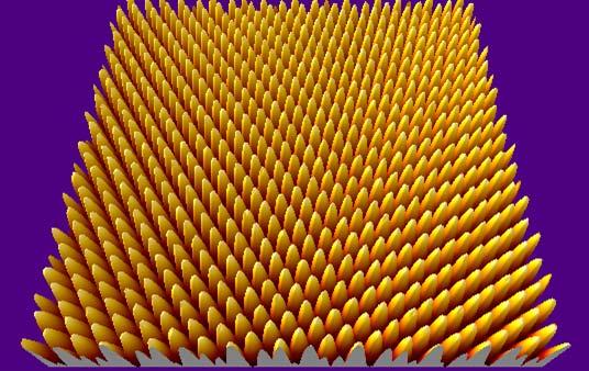
3 Patterned Media: Discrete Track vs. Bit Patterned Media Conventional PMR Media Continuous granular recording layer Multiple grains per bit Boundaries between bits determined by grains Thermal stability unit is 1 grain (~ 6 nm diam.) Discrete Track Media Conventional PMR media, with patterned tracks Multiple grains per bit Eliminates track edge noise and reduces adjacent track interference Thermal stability unit is still 1 grain (~ 6 nm diam.) Bit Patterned Media Highly exchange coupled granular media Multiple grains per island, but each island is a single domain particle Bit locations determined by lithography Therm. stab. unit is 1 island (~15 nm diam.) 3
 430 Oe/nm periods λ 1 =λ 2 =25.")
4 Modeling a BPM Recording System pooled fabrication tolerance centroid jitter shape jitter pooled synchronization tolerance write synchronization jitter NRO, etc. areal density contours [Tb/in 2 ] σ print =3 nm switching field distribution of the islands Areal Density [Tb/in 2 ] 1 Tb/in 2 design example σh sw 1000 Oe grad(h eff ) 430 Oe/nm periods λ 1 =λ 2 =25.4 nm island size=17.9x17.9x8 nm 3 trenches γ 1 =γ 2 =7.4 nm E b 120 k B T disqualified region of parameter space due to readback jitter or thermal stability σ print =2 nm BER w =10-6 K 1 =2.7x10 5 J/m 3 realistic regime gradient of the effective write field profile thermal stability contours [K 1 V/k B T] at 300 K M. Schabes HGST 4
 BAR =1 Pitch = 25nm, Island size =18nm Fabrication")

5 Bit Patterned vs. Discrete Track Media: Examples at 1 Tbit/in2 Bit Patterned Media (BPM) BAR =1 Pitch = 25nm, Island size =18nm Fabrication tolerance: 1σ ~ 1 nm (size and placement) Discrete Track Media (DTM) BAR=4 Pitch = 47nm, land size = 33nm, groove = 14nm Requires very fine grain media BAR = 4 This BAR places tough demands on write head field and the servo system to due to the high tpi Down track pitch = 13nm, Island size = 9nm Tolerance = 1σ ~ 0.5 nm (size and placement) Even more aggressive patterning 5

6 Making Pattern Media: Ahead of the ITRS Roadmap ITRS Roadmap DRAM ½ Pitch (nm) nm 193 nm immersion with water 193 nm immersion with water 193 nm immersion with other fluids EUV, ML2 DRAM FLASH The semiconductor industry will not provide a lithography solution in 32 EUV 193 nm immersion with other fluids & lenses 193 nm with innovative immersion with water Imprint, ML2 time for patterned media EUV Innovative 193 nm immersion Imprint, ML2, Innovative Technology Innovative Technology Innovative EUV, Imprint, ML2, BPM PATTERNED MEDIA Research Required Development Underway Qualification Production Continuous Improvement 6
7 Some numbers to contemplate islands per disk smaller and denser features than used by the semiconductor industry 10 9 disks per year far higher than the total wafers/year by the semiconductor industry Low cost target < $5 per disk (total disk cost) A completely different approach is needed different process / different equipment double sided 7
 data tracks servo sector track")


8 Prepatterned Servo track direction (circumferential) data tracks servo sector track ID Gray code Very precise servo features created along with data track islands Eliminates need for separate servowriting operation Leads to multiple feature sizes in patterning quad burst tracking pattern 8
 Planarization Lube and Burnish 1 master (e-beam + self-assembly) 10,000 replicated nanoimprint templates Inspection 100,000,000 patterned disks 9")
9 Bit Patterned Media: A Potential Fabrication Overview Existing Processes New Processes Template Fabrication Rotary Stage E-Beam Patterning Directed Self-Assembly Master Template Fabrication Template Replication Media Fabrication Process Incoming disk substrate Deposition of magnetic layers Nanoimprint Pattern Transfer (i.e. Etching) Planarization Lube and Burnish 1 master (e-beam + self-assembly) 10,000 replicated nanoimprint templates Inspection 100,000,000 patterned disks 9
10 Technology Building Blocks for Patterned Media Want to look at what is needed for each of these key building blocks and show some examples of status. Will mainly use BPM as an example system but most of discussion is also relevant to DTM. Media Deposition Masks Patterning Lithography Metrology Planarization 10


11 Master Pattern Lithography Roadmap e-beam lithography e-beam prepattern + block copolymer self-assembly 300 Gbit/in 2 Write at twice the period 1 Tbit/in 2 pattern clean-up 1X density and self-assembly fills in the missing dots 4X density E. Dobisz - HGST R. Ruiz - HGST rotary stage e-beam e-beam + density multiplier Pattern density (Gbit/sq. inch) 11
 thin film Short range order: hexagonal close-pack Long range: disordered (without")
12 Beyond E-Beam: Self-Assembly of Block Copolymers Poly(styrene-block-methylmethacrylate) (PS-b-PMMA) thin film Short range order: hexagonal close-pack Long range: disordered (without guiding) 12
13 Pattern Clean-Up and Density Multiplication E-beam-generated chemical contrast patterns for directed self-assembly Pattern Rectification or Clean Up (1:1) Interpolation for Density Multiplication (4:1) Take an imperfect e-beam pattern Write at twice the period 1X density and improve spot uniformity via self-assembly and self-assembly fills in the missing dots 4X density R. Ruiz, H. Kang, F. A. Detcheverry, E. Dobisz, D. S. Kercher, T. R. Albrecht, J. J. de Pablo, P. F. Nealey, Science 2008, 321,

14 Pattern Density Multiplication (4:1 Guiding) E-beam pre-pattern Block Copolymer 39 nm period 78 nm period Dot Size Distribution σs=35nm2 σp=22nm2 54 nm period 27 nm period σs=39nm2 σp=13nm2 Hitachi Global Storage Technologies R. Ruiz, H. Kang, F. A. Detcheverry, E. Dobisz, D.2008 S. Kercher, T. R. Albrecht, J. J. de Pablo, P. F. Nealey, Science 2008, 321,


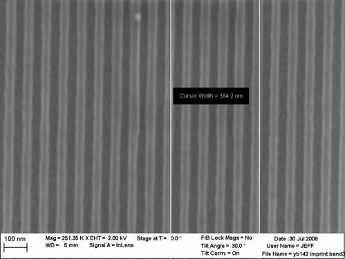
15 Long-range order R. Ruiz, H. Kang, F. A. Detcheverry, E. Dobisz, D. S. Kercher, T. R. Albrecht, J. J. de Pablo, P. F. Nealey, Science 2008, 321, 936. Density multiplication. 1Tb/in 2 L s =54nm; L p =27nm, σ x = 1.8nm, σ y = 1.0 nm Pattern Transfer to create Si Pillars 15
16 UV-Cure Nanoimprinting: Process Steps Graphic: Molecular Imprints, Inc. Resist dispensing (ink jet) Thin template is bowed so initial contact in the center of the disk Capillary forces pull template into conformal contact with the disk Expose with UV light to cure the imprint resist Separate template from disk Etch 16
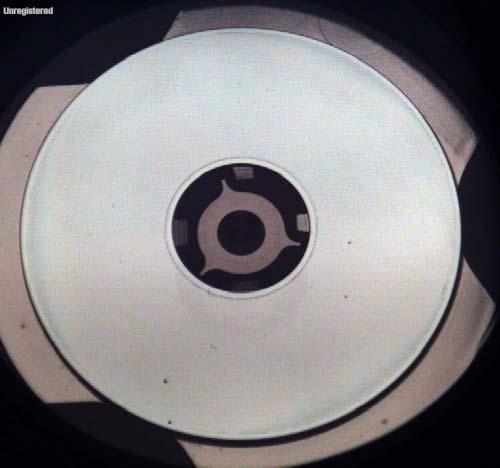

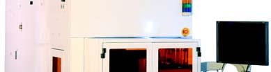
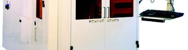

17 Nanoimprinting: Molecular Imprints Imprio 1100 Pitch = 76nm, 50nm resist thickness 300 Gbit/in 2 (50 nm period hcp) pattern 17
18 Nanoimprinting Requirements for Patterned Media Conformal full-disk (no stepping) imprinting of surface with imperfect flatness (65 95 mm diameter disks) Double-sided imprinting Single layer / no overlay / modest alignment (~10 um centering on disk) Mitigation of defects on both templates and imprinted disks High fidelity replication of nm-scale features with high aspect ratio Resist adhesion to disk Low-force release from template Template lifetime and template replication Resist etch resistance for pattern transfer Residual layer thickness and uniformity Resist etch selectivity for pattern transfer Clean removability of resist High throughput and low cost Industry: 1 billion(!) disks/year residual layer thickness substrate nanoimprint resist 18
19 Mask and Lithography: Key Requirements Masks (Some business model options here with vendors) High precision rotary e-beam tools Image multiplication methods (copolymers, side wall imaging ) BPM patterns with BAR > 1 Pattern transfer tooling for image into substrate Method to cheaply replicate the masters Metrology (image size, image shape, image placement, defects) Imprinting High speed double sided imprint tools Reasonable lifetime of templates Insensitivity to incoming defects/contamination Metrology (image size, image shape, image placement, defects) 19

 needs planarization 50 nm pitch J. Risner, O. Hellwig, E. Dobisz, D.")
20 Pattern Transfer Approach 1: Etched Substrate Island Trench 50 nm diameter islands 100 nm pitch Direct e-beam lithography Cr lift-off dots as hard mask Substrate RIE Blanket mag layer deposition Issues with substrate etch approach: GOOD: clean, fast etching (RIE) of friendly materials Si, SiO 2, Si 3 N 4 etch products volatile BAD: trench material is present possible noise source BAD: large topography (~40 nm) needs planarization 50 nm pitch J. Risner, O. Hellwig, E. Dobisz, D. Kercher - HGST 20
 of magnetic layer Issues with mag layer etch approach: BAD: dirty, slow etching (IBE) of unfriendly materials Co, Pd, Ni, etc.")
21 Approach 2: Etched Magnetic Film Hard Mask Material #2 Hard Mask Material #1 Co/Pd ML Underlayers Substrate 90 nm diameter islands 160 nm pitch Nanoimprint lithography RIE removal of resist residual layer RIE of hard mask layers RIE (or IBE) of magnetic layer Issues with mag layer etch approach: BAD: dirty, slow etching (IBE) of unfriendly materials Co, Pd, Ni, etc. redeposition of nonvolatile products GOOD: no trench material GOOD: less topography BAD: possible edge damage due to ion bombardment, Strip of masks directly on media 21
22 Media patterning: Key Requirements Patterning High Speed double sided etch tools (800 dph) Ability to deal with either patterned media or patterned substrate concept Selectivity between mask and media Multiple etch steps/processes insitu and all vacuum based A clean mask strip process without media damage Temperature rise/cooling issue at high etch rates No redeposition of etched material and or edge damage to features Uniform CD control and sharp feature profiles with multiple feature sizes End point control Metrology (image size, image shape, image placement, defects) 22
23 Head-Disk Interface: Motivation for Planarization Conventional Smooth Disk Patterned Disk ~5 nm flying slider motion FH sigma ~ 10% of FH disk surface FH falls sigma increases slightly insufficient clearance: crash Patterned Disk w/ Higher FH Planarized Patterned Disk Trenches filled ABS change to increase FH sigma increases further behaves like conventional smooth disk low FH and tight sigma Lowest possible flying height (FH) and tight sigma essential for high density recording 23
24 Planarization: Key Requirements Planarization Low cost Concepts Deposition and etch Spin on and etch CMP Excellent planarization with no residual material left of top of media that impacts magnetic spacing. Ability to deal with multiple feature sizes. Planarization material consistent with HDD environment No contamination Ability to deal with either patterned media or patterned substrate concept End point control Metrology (planarity, defects) 24
25 Metrology: Key Requirements (at 1 Tbit in/2) Huge volumes of parts of media and templates Features < 12nm, 2:1 aspect ratios Placement 1 sigma < 1nm Multiple types of materials/substrates (glass, polymer, media) Process control (CD, placement, profile control) Lithography Etch Planarization Defect control (10 13 features per disks) Over several size ranges Catch small repeating defects in master and daughters Catch random tool induced defects in timely fashion to allow correction Extendibility 25

26 Bit Patterned Media: Summary Patterned Media (both DTM and BPM) are potential solutions for extending the areal density growth of magnetic data recording beyond the approaching limits of conventional media Likely fabrication strategy Master pattern generation by high resolution e-beam lithography and self-assembly Pattern replication by UV-cure nanoimprint lithography (the only viable lithography solution) Etching of disk substrate or mag layer Tight fabrication tolerances required: small feature and sigmas High quality master template Pattern multiplication needed to go beyond e-beam lithography Nanoimprint requirements for patterned media fabrication Full-disk conformal imprinting on both sides High yield / low defect rate but no overlay required! Patterning tools are novel in terms of High throughput and dual sided processing Potentially difficult materials to etch in high density patterns Metrology Need new concepts given the volume of disks and minimum feature sizes in play Magnetic layer optimization (not discussed) DTM: Small grain media BPM: Tight switching field distribution (SFD) required 26
Achieving Tight sigmas in Bit Patterned Media
 Achieving Tight sigmas in Bit Patterned Media Dieter Weller Chief Technologist Seagate Technology Diskcon 2008, September 18, Santa Clara Acknowledgement 1 Tbit/in 2 patterned dots Team Seagate Areal Density
Anisotropy Distributions in Patterned Magnetic Media
 MINT Review & Workshop 24-25 Oct. 2006 Anisotropy Distributions in Patterned Magnetic Media Tom Thomson Hitachi San Jose Research Center Page 1 Acknowledgements Manfred Albrecht (Post-doc) Tom Albrecht
Technologies VII. Alternative Lithographic PROCEEDINGS OF SPIE. Douglas J. Resnick Christopher Bencher. Sponsored by. Cosponsored by.
 PROCEEDINGS OF SPIE Alternative Lithographic Technologies VII Douglas J. Resnick Christopher Bencher Editors 23-26 February 2015 San Jose, California, United States Sponsored by SPIE Cosponsored by DNS
CURRENT STATUS OF NANOIMPRINT LITHOGRAPHY DEVELOPMENT IN CNMM
 U.S. -KOREA Forums on Nanotechnology 1 CURRENT STATUS OF NANOIMPRINT LITHOGRAPHY DEVELOPMENT IN CNMM February 17 th 2005 Eung-Sug Lee,Jun-Ho Jeong Korea Institute of Machinery & Materials U.S. -KOREA Forums
Nanoimprint Lithography
 Nanoimprint Lithography Wei Wu Quantum Science Research Advanced Studies HP Labs, Hewlett-Packard Email: wei.wu@hp.com Outline Background Nanoimprint lithography Thermal based UV-based Applications based
2D Coding and Iterative Detection Schemes
 2D Coding and Iterative Detection Schemes J. A. O Sullivan, N. Singla, Y. Wu, and R. S. Indeck Washington University Magnetics and Information Science Center Nanoimprinting and Switching of Patterned Media
Three Approaches for Nanopatterning
 Three Approaches for Nanopatterning Lithography allows the design of arbitrary pattern geometry but maybe high cost and low throughput Self-Assembly offers high throughput and low cost but limited selections
ADVANCED STORAGE TECHNOLOGY CONSORTIUM RESEARCH PROPOSAL TEMPLATE
 ADVANCED STORAGE TECHNOLOGY CONSORTIUM RESEARCH PROPOSAL TEMPLATE RADIALLY ORDERED BIT PATTERNED MEDIA USING A COMBINATION OF NANOIMPRINT LITHOGRAPHY AND SELF-ASSEMBLY AND FABRICATION OF PATTERN MEDIA
Simulation of Ion Beam Etching of Patterned Nanometer-scale Magnetic Structures for High-Density Storage Applications
 Engineered Excellence A Journal for Process and Device Engineers Simulation of Ion Beam Etching of Patterned Nanometer-scale Magnetic Structures for High-Density Storage Applications Introduction Fabrication
Enhanced Magnetic Properties of Bit Patterned Magnetic Recording Media by Trench-Filled Nanostructure
 CMRR Report Number 32, Summer 2009 Enhanced Magnetic Properties of Bit Patterned Magnetic Recording Media by Trench-Filled Nanostructure Edward Chulmin Choi, Daehoon Hong, Young Oh, Leon Chen, Sy-Hwang
SEMATECH Knowledge Series 2010
 SEMATECH Knowledge Series 2010 Summary of the SEMATECH Workshop on Directed Self Assembly Lloyd Litt SEMATECH/GF Bill Hinsberg - IBM 20 October 2010 Kobe, Japan Copyright 2010 Advanced Materials Research
Lithography Challenges Moore s Law Rising Costs and Challenges of Advanced Patterning
 Lithography Challenges Moore s Law Rising Costs and Challenges of Advanced Patterning SEMI Texas Spring Forum May 21, 2013 Austin, Texas Author / Company / Division / Rev. / Date A smartphone today has
Fiducial Marks for EUV mask blanks. Jan-Peter Urbach, James Folta, Cindy Larson, P.A. Kearney, and Thomas White
 Fiducial Marks for EUV mask blanks Jan-Peter Urbach, James Folta, Cindy Larson, P.A. Kearney, and Thomas White Fiducial marks are laser scribed on 200 mm wafers to enable defect registration on metrology
Introduction to magnetic recording + recording materials
 Introduction to magnetic recording + recording materials Laurent Ranno Institut Néel, Nanoscience Dept, CNRS-UJF, Grenoble, France I will give two lectures about magnetic recording. In the first one, I
UNIT 3. By: Ajay Kumar Gautam Asst. Prof. Dev Bhoomi Institute of Technology & Engineering, Dehradun
 UNIT 3 By: Ajay Kumar Gautam Asst. Prof. Dev Bhoomi Institute of Technology & Engineering, Dehradun 1 Syllabus Lithography: photolithography and pattern transfer, Optical and non optical lithography, electron,
MICRO AND NANOPROCESSING TECHNOLOGIES
 LECTURE 5 MICRO AND NANOPROCESSING TECHNOLOGIES Introduction Ion lithography X-ray lithography Soft lithography E-beam lithography Concepts and processes Lithography systems Masks and resists Chapt.9.
Techniken der Oberflächenphysik (Techniques of Surface Physics)
") Techniken der Oberflächenphysik (Techniques of Surface Physics) Prof. Yong Lei & Dr. Yang Xu (& Liying Liang) Fachgebiet 3D-Nanostrukturierung, Institut für Physik Contact: yong.lei@tu-ilmenau.de; yang.xu@tu-ilmenau.de;
Techniken der Oberflächenphysik (Techniques of Surface Physics) Prof. Yong Lei & Dr. Yang Xu (& Liying Liang) Fachgebiet 3D-Nanostrukturierung, Institut für Physik Contact: yong.lei@tu-ilmenau.de; yang.xu@tu-ilmenau.de;
Supplementary Figure 1 Detailed illustration on the fabrication process of templatestripped
 Supplementary Figure 1 Detailed illustration on the fabrication process of templatestripped gold substrate. (a) Spin coating of hydrogen silsesquioxane (HSQ) resist onto the silicon substrate with a thickness
Fabrication of ordered array at a nanoscopic level: context
 Fabrication of ordered array at a nanoscopic level: context Top-down method Bottom-up method Classical lithography techniques Fast processes Size limitations it ti E-beam techniques Small sizes Slow processes
Passionately Innovating With Customers To Create A Connected World
 Passionately Innovating With Customers To Create A Connected World Multi Die Integration Can Material Suppliers Meet the Challenge? Nov 14, 2012 Jeff Calvert - R&D Director, Advanced Packaging Technologies
UHF-ECR Plasma Etching System for Dielectric Films of Next-generation Semiconductor Devices
 UHF-ECR Plasma Etching System for Dielectric Films of Next-generation Semiconductor Devices 1 UHF-ECR Plasma Etching System for Dielectric Films of Next-generation Semiconductor Devices Katsuya Watanabe
Future Magnetic Recording Technologies
 Future Magnetic Recording Technologies Seagate Research Areal Density Perspective Max. Areal Density (Gbit/in 2 ) 10000 1000 100 10 1 0.1 1 Tbit/in 2 LABORATORY DEMOS Products Historical 60% CGR line 1990
Overview of EUV Lithography and EUV Optics Contamination
 Accelerating the next technology revolution Overview of EUV Lithography and EUV Optics Contamination Andrea Wüest NIST Contamination WS Gaithersburg, MD June 2, 2009 Copyright 2008 SEMATECH, Inc. SEMATECH,
Lecture 14 Advanced Photolithography
 Lecture 14 Advanced Photolithography Chapter 14 Wolf and Tauber 1/74 Announcements Term Paper: You are expected to produce a 4-5 page term paper on a selected topic (from a list). Term paper contributes
Sensors and Metrology. Outline
 Sensors and Metrology A Survey 1 Outline General Issues & the SIA Roadmap Post-Process Sensing (SEM/AFM, placement) In-Process (or potential in-process) Sensors temperature (pyrometry, thermocouples, acoustic
Acknowledgements. Presentation Title Date 2
 Extensions of Perpendicular Recording Olle Heinonen and Kaizhong Gao Recording Head Operations Seagate Technology Acknowledgements We gratefully acknowledge contributions and learning from Mark Kief, Robert
Unconventional Nano-patterning. Peilin Chen
 Unconventional Nano-patterning Peilin Chen Reference Outlines History of patterning Traditional Nano-patterning Unconventional Nano-patterning Ancient Patterning "This is the Elks' land". A greeting at
Scanning Probe Microscopy. L. J. Heyderman
 1 Scanning Probe Microscopy 2 Scanning Probe Microscopy If an atom was as large as a ping-pong ball......the tip would have the size of the Matterhorn! 3 Magnetic Force Microscopy Stray field interaction
Introduction to / Status of Directed Self- Assembly
 Introduction to / Status of Directed Self- Assembly DSA Workshop, Kobe Japan, October 2010 Bill Hinsberg IBM Almaden Research Center San Jose CA 95120 hnsbrg@almaden.ibm.com 2010 IBM Corporation from Bringing
MSN551 LITHOGRAPHY II
 MSN551 Introduction to Micro and Nano Fabrication LITHOGRAPHY II E-Beam, Focused Ion Beam and Soft Lithography Why need electron beam lithography? Smaller features are required By electronics industry:
Nanostructure. Materials Growth Characterization Fabrication. More see Waser, chapter 2
 Nanostructure Materials Growth Characterization Fabrication More see Waser, chapter 2 Materials growth - deposition deposition gas solid Physical Vapor Deposition Chemical Vapor Deposition Physical Vapor
A Photonic Crystal Laser from Solution Based. Organo-Lead Iodide Perovskite Thin Films
 SUPPORTING INFORMATION A Photonic Crystal Laser from Solution Based Organo-Lead Iodide Perovskite Thin Films Songtao Chen 1, Kwangdong Roh 2, Joonhee Lee 1, Wee Kiang Chong 3,4, Yao Lu 5, Nripan Mathews
Hybrid Wafer Level Bonding for 3D IC
 Hybrid Wafer Level Bonding for 3D IC An Equipment Perspective Markus Wimplinger, Corporate Technology Development & IP Director History & Roadmap - BSI CIS Devices???? 2013 2 nd Generation 3D BSI CIS with
Lithography and Etching
 Lithography and Etching Victor Ovchinnikov Chapters 8.1, 8.4, 9, 11 Previous lecture Microdevices Main processes: Thin film deposition Patterning (lithography) Doping Materials: Single crystal (monocrystal)
Magnetic Recording. by Gaspare Varvaro. Istituto di Struttura della Materia CNR Nanostructured Magnetic Materials Group
 Magnetic Recording by Gaspare Varvaro Istituto di Struttura della Materia CNR Nanostructured Magnetic Materials Group Outline Brief History of Magnetic Recording Hard Disk Drives General Aspects (Longitudinal
Thin Wafer Handling Challenges and Emerging Solutions
 1 Thin Wafer Handling Challenges and Emerging Solutions Dr. Shari Farrens, Mr. Pete Bisson, Mr. Sumant Sood and Mr. James Hermanowski SUSS MicroTec, 228 Suss Drive, Waterbury Center, VT 05655, USA 2 Thin
PHI 5000 Versaprobe-II Focus X-ray Photo-electron Spectroscopy
 PHI 5000 Versaprobe-II Focus X-ray Photo-electron Spectroscopy The very basic theory of XPS XPS theroy Surface Analysis Ultra High Vacuum (UHV) XPS Theory XPS = X-ray Photo-electron Spectroscopy X-ray
Optical Measurements of Critical Dimensions at Several Stages of the Mask Fabrication Process
 Optical Measurements of Critical Dimensions at Several Stages of the Mask Fabrication Process John C. Lam, Alexander Gray n&k Technology, Inc., Santa Clara, CA ABSTRACT Critical dimension (CD) metrology
High NA the Extension Path of EUV Lithography. Dr. Tilmann Heil, Carl Zeiss SMT GmbH
 High NA the Extension Path of EUV Lithography Dr. Tilmann Heil, Carl Zeiss SMT GmbH Introduction This talk is about resolution. Resolution λ = k 1 NA High-NA NA 0.33 0.4 0.5 0.6 Resolution @ k1=0.3 single
UNIVERSITY OF CALIFORNIA College of Engineering Department of Electrical Engineering and Computer Sciences. Fall Exam 1
 UNIVERSITY OF CALIFORNIA College of Engineering Department of Electrical Engineering and Computer Sciences EECS 143 Fall 2008 Exam 1 Professor Ali Javey Answer Key Name: SID: 1337 Closed book. One sheet
01 Development of Hard Disk Drives
 01 Development of Hard Disk Drives Design Write / read operation MR / GMR heads Longitudinal / perpendicular recording Recording media Bit size Areal density Tri-lemma 11:00 10/February/2016 Wednesday
Neutron Reflectometry of Ferromagnetic Arrays
 Neutron Reflectometry of Ferromagnetic Arrays Z.Y. Zhao a, P. Mani a, V.V.Krishnamurthy a, W.-T. Lee b, F. Klose b, and G.J. Mankey a a Center for Materials for Information Technology and Department of
Development status of back-end process for UV-NIL template fabrication
 Development status of back-end process for UV-NIL template fabrication Yuichi Inazuki, Kimio Itoh, Sho Hatakeyama, Kouichirou Kojima, Masaaki Kurihara, Yasutaka Morikawa, Hiroshi Mohri and Naoya Hayashi
ECC Media Technology. 1. Introduction. 2. ECC Media. Shunji Takenoiri TuQiang Li Yoshiyuki Kuboki
 ECC Media Technology Shunji Takenoiri TuQiang Li Yoshiyuki Kuboki 1. Introduction Two years have already elapsed since Fuji Electric began mass-producing perpendicular magnetic recording media, and now
Spectroscopic Critical Dimension technology (SCD) for Directed Self Assembly
 for Directed Self Assembly") Spectroscopic Critical Dimension technology (SCD) for Directed Self Assembly Senichi Nishibe a, Thaddeus Dziura a, Venkat Nagaswami a, Roel Gronheid b a KLA-Tencor Corporation, 1 Technology Drive, Milpitas
Spectroscopic Critical Dimension technology (SCD) for Directed Self Assembly Senichi Nishibe a, Thaddeus Dziura a, Venkat Nagaswami a, Roel Gronheid b a KLA-Tencor Corporation, 1 Technology Drive, Milpitas
Critical Dimension Uniformity using Reticle Inspection Tool
 Critical Dimension Uniformity using Reticle Inspection Tool b Mark Wylie, b Trent Hutchinson, b Gang Pan, b Thomas Vavul, b John Miller, b Aditya Dayal, b Carl Hess a Mike Green, a Shad Hedges, a Dan Chalom,
Nanotechnology Fabrication Methods.
 Nanotechnology Fabrication Methods. 10 / 05 / 2016 1 Summary: 1.Introduction to Nanotechnology:...3 2.Nanotechnology Fabrication Methods:...5 2.1.Top-down Methods:...7 2.2.Bottom-up Methods:...16 3.Conclusions:...19
High-density data storage: principle
 High-density data storage: principle Current approach High density 1 bit = many domains Information storage driven by domain wall shifts 1 bit = 1 magnetic nanoobject Single-domain needed Single easy axis
Nanostructures Fabrication Methods
 Nanostructures Fabrication Methods bottom-up methods ( atom by atom ) In the bottom-up approach, atoms, molecules and even nanoparticles themselves can be used as the building blocks for the creation of
LECTURE 5 SUMMARY OF KEY IDEAS
 LECTURE 5 SUMMARY OF KEY IDEAS Etching is a processing step following lithography: it transfers a circuit image from the photoresist to materials form which devices are made or to hard masking or sacrificial
Towards nanoimprint lithography-aware layout design checking. 25 February 2010 Hayden Taylor and Duane Boning Massachusetts Institute of Technology
 Towards nanoimprint lithography-aware layout design checking 25 February 2010 Hayden Taylor and Duane Boning Massachusetts Institute of Technology Nanoimprint is the mechanical patterning of resist spun
S. Mangin 1, Y. Henry 2, D. Ravelosona 3, J.A. Katine 4, and S. Moyerman 5, I. Tudosa 5, E. E. Fullerton 5
 Spin transfer torques in high anisotropy magnetic nanostructures S. Mangin 1, Y. enry 2, D. Ravelosona 3, J.A. Katine 4, and S. Moyerman 5, I. Tudosa 5, E. E. Fullerton 5 1) Laboratoire de Physique des
Developer-soluble Gap fill materials for patterning metal trenches in Via-first Dual Damascene process
 Developer-soluble Gap fill materials for patterning metal trenches in Via-first Dual Damascene process Mandar Bhave, Kevin Edwards, Carlton Washburn Brewer Science, Inc., 2401 Brewer Dr., Rolla, MO 65401,
Lecture 8. Photoresists and Non-optical Lithography
 Lecture 8 Photoresists and Non-optical Lithography Reading: Chapters 8 and 9 and notes derived from a HIGHLY recommended book by Chris Mack, Fundamental Principles of Optical Lithography. Any serious student
Nova 600 NanoLab Dual beam Focused Ion Beam IITKanpur
 Nova 600 NanoLab Dual beam Focused Ion Beam system @ IITKanpur Dual Beam Nova 600 Nano Lab From FEI company (Dual Beam = SEM + FIB) SEM: The Electron Beam for SEM Field Emission Electron Gun Energy : 500
EV Group. Enabling processes for 3D interposer. Dr. Thorsten Matthias EV Group
 EV Group Enabling processes for 3D interposer Dr. Thorsten Matthias EV Group EV Group in a Nutshell st Our philosophy Our mission in serving next generation application in semiconductor technology Equipment
JOHN G. EKERDT RESEARCH FOCUS
 JOHN G. EKERDT RESEARCH FOCUS We study the surface, growth and materials chemistry of metal, dielectric, ferroelectric, and polymer thin films. We seek to understand and describe nucleation and growth
Pattern Transfer- photolithography
 Pattern Transfer- photolithography DUV : EUV : 13 nm 248 (KrF), 193 (ArF), 157 (F 2 )nm H line: 400 nm I line: 365 nm G line: 436 nm Wavelength (nm) High pressure Hg arc lamp emission Ref: Campbell: 7
High-resolution Characterization of Organic Ultrathin Films Using Atomic Force Microscopy
 High-resolution Characterization of Organic Ultrathin Films Using Atomic Force Microscopy Jing-jiang Yu Nanotechnology Measurements Division Agilent Technologies, Inc. Atomic Force Microscopy High-Resolution
Optical Proximity Correction
 Optical Proximity Correction Mask Wafer *Auxiliary features added on mask 1 Overlay Errors + + alignment mask wafer + + photomask plate Alignment marks from previous masking level 2 (1) Thermal run-in/run-out
MRAM: Device Basics and Emerging Technologies
 MRAM: Device Basics and Emerging Technologies Matthew R. Pufall National Institute of Standards and Technology 325 Broadway, Boulder CO 80305-3337 Phone: +1-303-497-5206 FAX: +1-303-497-7364 E-mail: pufall@boulder.nist.gov
Cost of Ownership Considerations for Maskless Lithography
 Accelerating the next technology revolution Cost of Ownership Considerations for Maskless Lithography Lloyd C. Litt, SEMATECH Andrea F. Wüest, SEMATECH Copyright 2008 SEMATECH, Inc. SEMATECH, and the SEMATECH
Selective Processes: Challenges and Opportunities in Semiconductor Scaling
 Selective Processes: Challenges and Opportunities in Semiconductor Scaling June 4, 2018 Kandabara Tapily TEL Technology Center, America, LLC IITC 2018 Selective Deposition Workshop K. Tapily/ IITC 2018
SHRINK. STACK. INTEGRATE.
 SHRINK. STACK. INTEGRATE. SUSS MICROTEC PRODUCT PORTFOLIO SHAPING THE FUTURE With more than 60 years of engineering experience SUSS MicroTec is a leading supplier of process equipment for microstructuring
Functional Materials for Advanced Patterning Robert D. Allen. IBM Almaden Research Center
 Functional Materials for Advanced Patterning Robert D. Allen Business Unit or Product Name IBM Almaden Research Center 2003 IBM Corporation Resists/Materials for Advanced Patterning Trends in Lithography
custom reticle solutions
 custom reticle solutions 01 special micro structures Pyser Optics has over 60 years experience in producing high quality micro structure products. These products are supplied worldwide to industries including
High Optical Density Photomasks For Large Exposure Applications
 High Optical Density Photomasks For Large Exposure Applications Dan Schurz, Warren W. Flack, Makoto Nakamura Ultratech Stepper, Inc. San Jose, CA 95134 Microlithography applications such as advanced packaging,
Model 2300XP PSL & Process-Particle Wafer Deposition System
 Model 2300XP PSL & Process-Particle Wafer Deposition System Deposit PSL spheres on wafers to create NISTtraceable PSL size standards for - calibrating wafer inspection systems - providing fab-wide and
1
 Process methodologies for temporary thin wafer handling solutions By Justin Furse, Technology Strategist, Brewer Science, Inc. Use of temporary bonding/debonding as part of thin wafer handling processes
Supplementary Information. Light Manipulation for Organic Optoelectronics Using Bio-inspired Moth's Eye. Nanostructures
 Supplementary Information Light Manipulation for Organic Optoelectronics Using Bio-inspired Moth's Eye Nanostructures Lei Zhou, Qing-Dong Ou, Jing-De Chen, Su Shen, Jian-Xin Tang,* Yan-Qing Li,* and Shuit-Tong
Cost Implications of EUV Lithography Technology Decisions
 Accelerating the next technology revolution Cost Implications of EUV Lithography Technology Decisions Andrea F. Wüest, SEMATECH Andrew J. Hazelton, Nikon Corporation Greg Hughes, SEMATECH Lloyd C. Litt,
Figure 1: Graphene release, transfer and stacking processes. The graphene stacking began with CVD
 Supplementary figure 1 Graphene Growth and Transfer Graphene PMMA FeCl 3 DI water Copper foil CVD growth Back side etch PMMA coating Copper etch in 0.25M FeCl 3 DI water rinse 1 st transfer DI water 1:10
Electrostatic Discharge (ESD) Breakdown between a Recording Head and a Disk with an Asperity
 Breakdown between a Recording Head and a Disk with an Asperity") Electrostatic Discharge (ESD) Breakdown between a Recording Head and a Disk with an Asperity Al Wallash and Hong Zhu Hitachi Global Storage Technologies San Jose, CA Outline Background Purpose Experimental
Electrostatic Discharge (ESD) Breakdown between a Recording Head and a Disk with an Asperity Al Wallash and Hong Zhu Hitachi Global Storage Technologies San Jose, CA Outline Background Purpose Experimental
Fabrication and Domain Imaging of Iron Magnetic Nanowire Arrays
 Abstract #: 983 Program # MI+NS+TuA9 Fabrication and Domain Imaging of Iron Magnetic Nanowire Arrays D. A. Tulchinsky, M. H. Kelley, J. J. McClelland, R. Gupta, R. J. Celotta National Institute of Standards
Structuring and bonding of glass-wafers. Dr. Anke Sanz-Velasco
 Structuring and bonding of glass-wafers Dr. Anke Sanz-Velasco Outline IMT Why glass? Components for life science Good bond requirements and evaluation Wafer bonding 1. Fusion bonding 2. UV-adhesive bonding
ETCHING Chapter 10. Mask. Photoresist
 ETCHING Chapter 10 Mask Light Deposited Substrate Photoresist Etch mask deposition Photoresist application Exposure Development Etching Resist removal Etching of thin films and sometimes the silicon substrate
GMR Read head. Eric Fullerton ECE, CMRR. Introduction to recording Basic GMR sensor Next generation heads TMR, CPP-GMR UCT) Challenges ATE
 Challenges ATE") GMR Read head Eric Fullerton ECE, CMRR Introduction to recording Basic GMR sensor Next generation heads TMR, CPP-GMR UCT) Challenges ATE 1 Product scaling 5 Mbyte 100 Gbyte mobile drive 8 Gbyte UCT) ATE
GMR Read head Eric Fullerton ECE, CMRR Introduction to recording Basic GMR sensor Next generation heads TMR, CPP-GMR UCT) Challenges ATE 1 Product scaling 5 Mbyte 100 Gbyte mobile drive 8 Gbyte UCT) ATE
Chapter 3 : ULSI Manufacturing Technology - (c) Photolithography
 Photolithography") Chapter 3 : ULSI Manufacturing Technology - (c) Photolithography 1 Reference 1. Semiconductor Manufacturing Technology : Michael Quirk and Julian Serda (2001) 2. - (2004) 3. Semiconductor Physics and Devices-
Chapter 3 : ULSI Manufacturing Technology - (c) Photolithography 1 Reference 1. Semiconductor Manufacturing Technology : Michael Quirk and Julian Serda (2001) 2. - (2004) 3. Semiconductor Physics and Devices-
Nano fabrication by e-beam lithographie
 Introduction to nanooptics, Summer Term 2012, Abbe School of Photonics, FSU Jena, Prof. Thomas Pertsch Nano fabrication by e-beam lithographie Lecture 14 1 Electron Beam Lithography - EBL Introduction
CUSTOM RETICLE SOLUTIONS
 CUSTOM RETICLE SOLUTIONS Special Micro Structures Pyser-SGI has over 60 years experience in producing high quality micro structure products. These products are supplied worldwide to industries including
Nanostrukturphysik (Nanostructure Physics)
") Nanostrukturphysik (Nanostructure Physics) Prof. Yong Lei & Dr. Yang Xu Fachgebiet 3D-Nanostrukturierung, Institut für Physik Contact: yong.lei@tu-ilmenau.de; yang.xu@tu-ilmenau.de Office: Unterpoerlitzer
Nanostrukturphysik (Nanostructure Physics) Prof. Yong Lei & Dr. Yang Xu Fachgebiet 3D-Nanostrukturierung, Institut für Physik Contact: yong.lei@tu-ilmenau.de; yang.xu@tu-ilmenau.de Office: Unterpoerlitzer
Electron-beam SAFIER process and its application for magnetic thin-film heads
 Electron-beam SAFIER process and its application for magnetic thin-film heads XiaoMin Yang, a) Harold Gentile, Andrew Eckert, and Stanko R. Brankovic Seagate Research Center, 1251 Waterfront Place, Pittsburgh,
Wafer Charging in Process Equipment and its Relationship to GMR Heads Charging Damage
 Wafer Charging in Process Equipment and its Relationship to GMR Heads Charging Damage Wes Lukaszek Wafer Charging Monitors, Inc. 127 Marine Road, Woodside, CA 94062 tel.: (650) 851-9313, fax.: (650) 851-2252,
process dependencies in nanoimprint
 Modeling and mitigating pattern and process dependencies in nanoimprint lithography 23 June 2011 Hayden Taylor Singapore-MIT Alliance for Research and Technology formerly based at: Microsystems Technology
Self-study problems and questions Processing and Device Technology, FFF110/FYSD13
 Self-study problems and questions Processing and Device Technology, FFF110/FYSD13 Version 2016_01 In addition to the problems discussed at the seminars and at the lectures, you can use this set of problems
HDD Reliability Modeling and Failure Prediction
 HDD Reliability Modeling and Failure Prediction (IDEMA Reliability Symposium, Dec. 6/05) Andrei Khurshudov, George Tyndall, Brian Strom, Sungchang Lee Samsung Information Systems America San Jose R&D Center
EE 527 MICROFABRICATION. Lecture 25 Tai-Chang Chen University of Washington
 EE 527 MICROFABRICATION Lecture 25 Tai-Chang Chen University of Washington ION MILLING SYSTEM Kaufmann source Use e-beam to strike plasma A magnetic field applied to increase ion density Drawback Low etch
TRANSVERSE SPIN TRANSPORT IN GRAPHENE
 International Journal of Modern Physics B Vol. 23, Nos. 12 & 13 (2009) 2641 2646 World Scientific Publishing Company TRANSVERSE SPIN TRANSPORT IN GRAPHENE TARIQ M. G. MOHIUDDIN, A. A. ZHUKOV, D. C. ELIAS,
I. NANOFABRICATION O AND CHARACTERIZATION Chap. 2 : Self-Assembly
 I. Nanofabrication and Characterization : TOC I. NANOFABRICATION O AND CHARACTERIZATION Chap. 1 : Nanolithography Chap. 2 : Self-Assembly Chap. 3 : Scanning Probe Microscopy Nanoscale fabrication requirements
EV Group. Engineered Substrates for future compound semiconductor devices
 EV Group Engineered Substrates for future compound semiconductor devices Engineered Substrates HB-LED: Engineered growth substrates GaN / GaP layer transfer Mobility enhancement solutions: III-Vs to silicon
Supplementary Information Our InGaN/GaN multiple quantum wells (MQWs) based one-dimensional (1D) grating structures
 based one-dimensional (1D) grating structures") Polarized white light from hybrid organic/iii-nitrides grating structures M. Athanasiou, R. M. Smith, S. Ghataora and T. Wang* Department of Electronic and Electrical Engineering, University of Sheffield,
Polarized white light from hybrid organic/iii-nitrides grating structures M. Athanasiou, R. M. Smith, S. Ghataora and T. Wang* Department of Electronic and Electrical Engineering, University of Sheffield,
Nano-Lithography. Edited by Stefan Landis
 Nano-Lithography Edited by Stefan Landis IST^ m WILEY Table of Contents Foreword Jörge DE SOUSA NORONHA Introduction Michel BRILLOUET xi xvii Chapter 1. X-ray Lithography: Fundamentals and Applications
Supplementary Materials for
 advances.sciencemag.org/cgi/content/full/1/10/e1500751/dc1 Supplementary Materials for Uniform metal nanostructures with long-range order via three-step hierarchical self-assembly The PDF file includes:
The Removal of Nanoparticles from Nanotrenches Using Megasonics
 NSF Center for Micro and Nanoscale Contamination Control The Removal of Nanoparticles from Nanotrenches Using Megasonics Pegah Karimi 1, Tae Hoon Kim 1, Ahmed A. Busnaina 1 and Jin Goo Park 2 1 NSF Center
J. Photopolym. Sci. Technol., Vol. 22, No. 5, Fig. 1. Orthogonal solvents to conventional process media.
 originates from the limited number of options regarding orthogonal solvents, i.e. solvents that do not dissolve or adversely damage a pre-deposited organic materials layer. The simplest strategy to achieve
Lecture 0: Introduction
 Lecture 0: Introduction Introduction q Integrated circuits: many transistors on one chip q Very Large Scale Integration (VLSI): bucketloads! q Complementary Metal Oxide Semiconductor Fast, cheap, low power
Nano Engineering & Storage Technology
 Nano Engineering & Storage Technology Group Research Presentation Tom Thomson Nano Engineering & Storage Technology Group School of Computer Science University of Manchester http://nest.cs.manchester.ac.uk/
STANDARD: SPECIFICATION FOR PROTECTIVE ENCLOSURE AND CARRIER SYSTEMS USED TO TRANSPORT AND STORE ( INCH EUV RETICLES
 Entegris Edit -SEMI Draft Document (10-11-2006 Revision) NEW STANDARD: SPECIFICATION FOR PROTECTIVE ENCLOSURE AND CARRIER SYSTEMS USED TO TRANSPORT AND STORE 6 INCH EUV RETICLES This specification draft
FLCC Seminar. Spacer Lithography for Reduced Variability in MOSFET Performance
 1 Seminar Spacer Lithography for Reduced Variability in MOSFET Performance Prof. Tsu-Jae King Liu Electrical Engineering & Computer Sciences Dept. University of California at Berkeley Graduate Student:
Patterning Challenges and Opportunities: Etch and Film
 Patterning Challenges and Opportunities: Etch and Film Ying Zhang, Shahid Rauf, Ajay Ahatnagar, David Chu, Amulya Athayde, and Terry Y. Lee Applied Materials, Inc. SEMICON, Taiwan 2016 Sept. 07-09, 2016,