Welsh Centre for Printing and Coating. College of Engineering
|
|
|
- Cornelius Dalton
- 5 years ago
- Views:
Transcription

1 Welsh Centre for Printing and Coating College of Engineering

2 Welsh Centre for Printing and Coating Potential applications for plasma functionalised GNP s for active packaging Tim Claypole a, Chris Spacie b, Ray Gibbs b a Welsh Centre for Printing and Coating, Swansea, UK b Haydale Graphene Industries, Ammanford, UK College of Engineering

3 Welsh Centre for Printing and Coating Centre of excellence for Printing and Coating - Open access centre - Comprehensive laboratories - Product Development - Fundamental research - Underpinning science Winner of the 2009 Regiostar s award for technology - Education and training - Technology transfer


4 Swansea University Bay Campus Opened August 2015 Printing R2R and sheet fed - bench scale to customer acceptance trials Ink formulation to pilot scale production Analysis of materials and prints
5 Listed on London Stock Exchange 14 th April 2014 Raised $10m for expansion in 2014 and on 2 nd November a further $9m for commercialisation. Post money valuation is $40m Now have centres of excellence in USA and Far East Acquired a composites business in November 2014 Focussed on plasma treatment of Graphenes and other nano materials that adds compatible chemical groups to ensure homogeneous dispersion An enabling technology focussed on Composites Inks/Paints and technical coatings Energy storage HGI
6 Graphite
7 Nano Carbons Type Carbon Layers Properties/Applications Typical cost ($/KG) Commercially available Epitaxial CVD 1-2 Conductive/almost Transparent/ITO? High end electronics FLG 3-10 Conductor/flexible/very high surface area/sensors GNPs Composites/Inks and coatings/lubricants/printing GO various Insulator- semiconductor? Hydrophillic-dispersions Defects and voids Graphite 100+ Lubricants/Refactories/brake s/engineering materials High- +10,000 CVD systems- Scale up? Cost! 200-2,000 Yesconsistency? Yes- variable product 200-2,000 In Part 3-20 Established >70,000mt pa
8 The Graphene Challenge Graphene as a carbon is relatively inert Properties not realised unless dispersed and bonded Tailored functionalisation is crucial for dispersion Structural integrity must be maintained Production must be repeatable and cost effective Production route must be scalable Environmental impact must be minimal
9 Functionalisation Carbon is its various forms including CNT and GNP is inert. Thus carbon is difficult to bond to and to disperse. Adding free radicals to the surface of the carbons can : exfoliate sheets enhance particle segregation improve dispersion enabled tailored interactions


10 Typical acid treated CNTs and GNPs Choice of functionalisation is limited to the acid groups used Harsh acid treatments are costly and environmentally unfavourable Acid Reflux breaks up nano carbon agglomerates but leaves acid residues Boiling fullerenes in acid with ultrasound can significantly damage aspect ratios

11 Plasma treated CNTs and GNPs

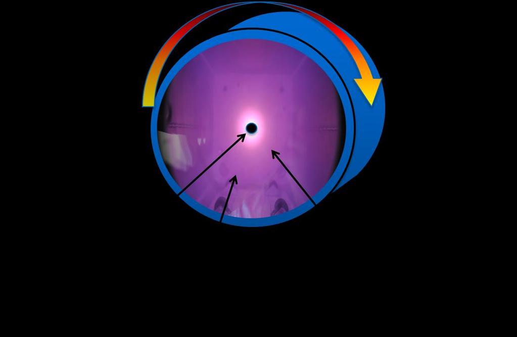
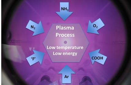
12 HAYDALE PLASMA TECHNOLOGY
 interact with the")

13 HAYDALE PLASMA PROCESSING Low pressure gas plasma generated from controlled gas and vapour mixtures Functionalisation: Ionised gases (plasma) interact with the CNT / GNP surface, disassociated molecules readily bond with a surface Cleaning : Reactive electrons and ions bombard the material surface removing contamination

14 DISPERSION IMPROVEMENTS Functionalisation and Dispersion HDPlas MWCNT in Oil As supplied MWCNT in Oil 14

15 3 levels of customisation One material and limited functionalisation will not fit all applications! 15

16 Projects with Haydale Applications for functionalised Carbon nano materials High precision manufacture PV Printable electronics Batteries Sensors Membrane Graphene based inks & coatings Optimisation Consistency Manufacturing SOP QA requirements Functionalised Nano Carbon composites Control of complex rheology during production Microscale modelling of electrical, thermal and mechanical properties of composites


17 GNP Inks Advantages: More environmentally friendly than silver Higher resistance per unit area Lower cost per ohm Applications Conductive tracks Strain gauges Piezo resistive Heaters Batteries, supercaps PV

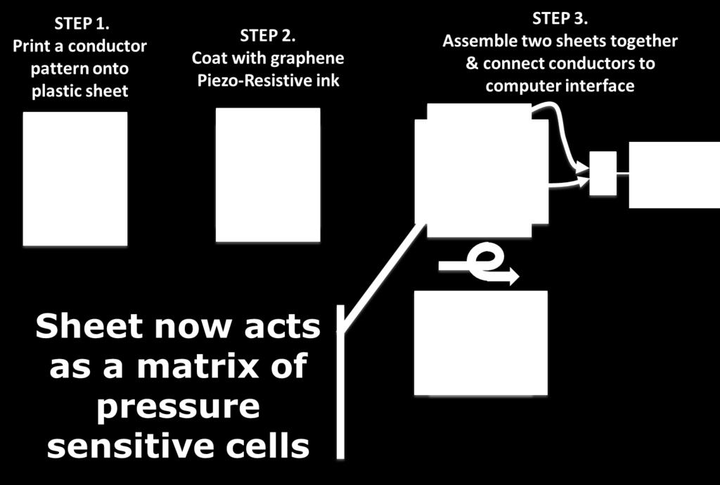
18 Pressure sensor


19 Advantages Low cost Thinner than a credit card Flexible Any size/shape Wide pressure range Real-time Applications: Security, Health care, Sports training, Industrial Measurement, Retail footfall, Smart packaging

20 CNT TFT Carbon Nanotube based Thin Film Transistors printed by flexography Field effect devices CNT as semiconductive layer Flexo printed CNT TFT Flexographic printing process
21 Graphene Summary Epitaxial single layer, high price, no route yet to volume scale up FLG has future potential GNP High volume, scalable Compatible with recycling Graphene is relatively inert Functionalisation Enables dispersion Adds functionality Could be applied to other nano and micro materials Applications Printed electronics conductive inks, sensors, integrate with Si Active coatings
22 Welsh Centre for Printing and Coating WCPC
Enhancing Composite Materials with Functionalized Graphene & CNTs Haydale Technologies Thailand (HTT) November 9, 2016
 November 9, 2016") Enhancing Composite Materials with Functionalized Graphene & CNTs Haydale Technologies Thailand (HTT) November 9, 2016 Brief Overview of HTT HAYDALE TECHNOLOGIES (THAILAND), is a subsidiary of Haydale
Enhancing Composite Materials with Functionalized Graphene & CNTs Haydale Technologies Thailand (HTT) November 9, 2016 Brief Overview of HTT HAYDALE TECHNOLOGIES (THAILAND), is a subsidiary of Haydale
Potential for energy storage applications with supercapacitor technology. Chris Stirling, Development Manager - Energy, Haydale Ltd.
 Potential for energy storage applications with supercapacitor technology. Chris Stirling, Development Manager - Energy, Haydale Ltd. Cambridge Graphene Technology Days 2015 3 rd CIR Graphene Business Conference,
Haydale and Composite Pressure Vessel Innovations. Dr Mark Lidgett Engineering Manager
 Haydale and Composite Pressure Vessel Innovations Dr Mark Lidgett Engineering Manager 13 th March 2018 Contents Company Overview Haydale s History with Composite Pressure Vessels Haydale s Composite Pressure
An overview of the emerging graphene industry in the UK
 12 Graphene has attracted considerable funding from government for universities and academic-industry collaborations. The start up sector has been particularly active. Having had no home-grown opportunity
Liberating the Nanotube: From Lab to Large Scale Production
 Liberating the Nanotube: From Lab to Large Scale Production HVM MNT Expo 2006 - Cambridge 11 December Russell Clarke Carbon Nanomaterials Business Manager Thomas Swan & Co. Ltd. Introduction Thomas Swan
Graphene Global Outlook: Roadmap for applications and opportunities
 Graphene Global Outlook: Roadmap for applications and opportunities Anthony Schiavo Analyst Prepared for: Graphene Malaysia About Lux Research 2 Agenda Graphene landscape 2016 Roadmap for graphene adoption
Graphene Fundamentals and Emergent Applications
 Graphene Fundamentals and Emergent Applications Jamie H. Warner Department of Materials University of Oxford Oxford, UK Franziska Schaffel Department of Materials University of Oxford Oxford, UK Alicja
Wafer-scale fabrication of graphene
 Wafer-scale fabrication of graphene Sten Vollebregt, MSc Delft University of Technology, Delft Institute of Mircosystems and Nanotechnology Delft University of Technology Challenge the future Delft University
Graphene films on silicon carbide (SiC) wafers supplied by Nitride Crystals, Inc.
 wafers supplied by Nitride Crystals, Inc.") 9702 Gayton Road, Suite 320, Richmond, VA 23238, USA Phone: +1 (804) 709-6696 info@nitride-crystals.com www.nitride-crystals.com Graphene films on silicon carbide (SiC) wafers supplied by Nitride Crystals,
9702 Gayton Road, Suite 320, Richmond, VA 23238, USA Phone: +1 (804) 709-6696 info@nitride-crystals.com www.nitride-crystals.com Graphene films on silicon carbide (SiC) wafers supplied by Nitride Crystals,
Workshop II Nanomaterials Surfaces and Layers Commercialising Carbon Nanotubes
 Workshop II Nanomaterials Surfaces and Layers Commercialising Carbon Nanotubes Harry Swan, Carbon Nanomaterials Business Manager, Thomas Swan & Co. Ltd. Introduction Thomas Swan & Co. Ltd. Carbon Nanotubes
Processing and Applications of Carbon Nanotubes, Graphene, and Beyond
 Processing and Applications of Carbon Nanotubes, Graphene, and Beyond Professor Mark C. Hersam Department of Materials Science and Engineering Northwestern University http://www.hersam-group.northwestern.edu/
Imaging Carbon materials with correlative Raman-SEM microscopy. Introduction. Raman, SEM and FIB within one chamber. Diamond.
 Imaging Carbon materials with correlative Raman-SEM microscopy Application Example Carbon materials are widely used in many industries for their exceptional properties. Electric conductance, light weight,
Towards Graphene-Based Printed Electronics Haydale Technologies Thailand (HTT)
") Towards Graphene-Based Printed Electronics Haydale Technologies Thailand (HTT) J. Patrick Frantz, Director, 25 September 2017 Disclaimer This presentation document and its content (the Presentation ) has
Towards Graphene-Based Printed Electronics Haydale Technologies Thailand (HTT) J. Patrick Frantz, Director, 25 September 2017 Disclaimer This presentation document and its content (the Presentation ) has
IEC TC 113 Nanotechnology for electrical and electronic products and systems
 IEC TC 113 Nanotechnology for electrical and electronic products and systems Mike Leibowitz TC 113 USNC TAG Secretary mike.leibowitz@nema.org February 28, 2017 ANSI NSP Arlington, VA - Background - Liaisons
New Materials and New Applications
 New Materials and New Applications Craig Lawrance Technical Manager, Textile Centre of Excellence craiglawrance@textile training.com 31st January 2018 6th Thematic Presentation, Huddersfield, UK Textile
 IMG: CORE-Materials Graphene tubes can be added into all three battery parts; anode, cathode and electrolyte. It improves different attributes of the device including speed of charging and discharging
Introducing the RoVaCBE Flagship project: Roll-to-roll Vacuum-processed Carbon Based Electronics. Dr Hazel Assender, University of Oxford
 Introducing the RoVaCBE Flagship project: Roll-to-roll Vacuum-processed Carbon Based Electronics Dr Hazel Assender, University of Oxford DALMATIAN TECHNOLOGY 21 st Sept 2010 1 Organic electronics Opportunity
2D MBE Activities in Sheffield. I. Farrer, J. Heffernan Electronic and Electrical Engineering The University of Sheffield
 2D MBE Activities in Sheffield I. Farrer, J. Heffernan Electronic and Electrical Engineering The University of Sheffield Outline Motivation Van der Waals crystals The Transition Metal Di-Chalcogenides
TABLE OF CONTENTS 1 RESEARCH METHODOLOGY Investment analysis Market impediment analysis EXECUTIVE SUMMARY...
 TABLE OF CONTENTS 1 RESEARCH METHODOLOGY... 22 1.1 Investment analysis...... 22 1.2 Market impediment analysis... 24 2 EXECUTIVE SUMMARY... 27 2.1 Products...... 27 2.2 Production in 2017...... 29 2.3
The Worlds Largest producer of Functionalised Doped and Decorated Graphitic nano structures current capacity circa 100 tonnes per annum
 "HVM Graphene+ 2014 Conference Oxford, UK 15 May www.hvm- uk.com The Worlds Largest producer of Functionalised Doped and Decorated Graphitic nano structures current capacity circa 100 tonnes per annum
Solutions for Assignment-8
 Solutions for Assignment-8 Q1. The process of adding impurities to a pure semiconductor is called: [1] (a) Mixing (b) Doping (c) Diffusing (d) None of the above In semiconductor production, doping intentionally
Session V: Graphene. Matteo Bruna CAMBRIDGE UNIVERSITY DEPARTMENT OF ENGINEERING
 Session V: Graphene Matteo Bruna Graphene: Material in the Flatland Graphite Graphene Properties: Thinnest imaginable material Good(and tunable) electrical conductor Strongest ever measured Stiffest known
Graphene, 2D Materials, and Carbon Nanotubes
 IDTechEx Research Graphene, 2D Materials, and Carbon Nanotubes 2018-2028 This report provides the most comprehensive and authoritative view of the topic, giving detailed ten-year market forecasts segmented
Nanotechnology in Consumer Products
 Nanotechnology in Consumer Products June 17, 2015 October 31, 2014 The webinar will begin at 1pm Eastern Time Perform an audio check by going to Tools > Audio > Audio Setup Wizard Chat Box Chat Box Send
A Reliable Supply Pla.orm for Graphene & non- carbon 2D Materials
 A Reliable Supply Pla.orm for Graphene & non- carbon 2D Materials Andy Goodwin Commercial Director Advanced Materials Cambridge Graphene Technology Days 2015 3 rd CIR Graphene Business Conference, 6 November
Overview. Carbon in all its forms. Background & Discovery Fabrication. Important properties. Summary & References. Overview of current research
 Graphene Prepared for Solid State Physics II Pr Dagotto Spring 2009 Laurene Tetard 03/23/09 Overview Carbon in all its forms Background & Discovery Fabrication Important properties Overview of current
The University of Manchester Advanced Materials
 The University of Manchester Advanced Materials Dr Kirk Malone Project Development Manager Sir Henry Royce Institute for Advanced Materials Associate Director for Industrial Partnerships EPSRC CDT in Materials
Optimization of MnO2 Electrodeposits using Graphenated Carbon Nanotube Electrodes for Supercapacitors
 Optimization of MnO2 Electrodeposits using Graphenated Carbon Nanotube Electrodes for Supercapacitors Waleed Nusrat, 100425398 PHY 3090U Material Science Thursday April 9 th 2015 Researchers optimize the
Nanoparticles for coatings. Why is reality so much less than the promise? Professor Steven Abbott R&T Director MacDermid Autotype Ltd
 Nanoparticles for coatings. Why is reality so much less than the promise? Professor Steven Abbott R&T Director MacDermid Autotype Ltd Background to the problem MacDermid Autotype make high quality coated
Carbon Nanomaterials: Nanotubes and Nanobuds and Graphene towards new products 2030
 Carbon Nanomaterials: Nanotubes and Nanobuds and Graphene towards new products 2030 Prof. Dr. Esko I. Kauppinen Helsinki University of Technology (TKK) Espoo, Finland Forecast Seminar February 13, 2009
Additive technologies for the patterning of fine metal tracks onto flexible substrates
 Additive technologies for the patterning of fine metal tracks onto flexible substrates Marc P.Y. Desmulliez m.desmulliez@hw.ac.uk MIcroSystems Engineering Centre (MISEC) Institute of Integrated Systems
Lectures Graphene and
 Lectures 15-16 Graphene and carbon nanotubes Graphene is atomically thin crystal of carbon which is stronger than steel but flexible, is transparent for light, and conducts electricity (gapless semiconductor).
Calculating Electronic Structure of Different Carbon Nanotubes and its Affect on Band Gap
 Calculating Electronic Structure of Different Carbon Nanotubes and its Affect on Band Gap 1 Rashid Nizam, 2 S. Mahdi A. Rizvi, 3 Ameer Azam 1 Centre of Excellence in Material Science, Applied Physics AMU,
Next Generation of Nano-Enhanced Composites and 3D Printable Materials. Dr. Elena Polyakova, CEO OTCQB: GPHBF TSX-V:GGG OTCQB: GPHBF
 Next Generation of Nano-Enhanced Composites and 3D Printable Materials Dr. Elena Polyakova, CEO Forward Looking Statements Information set forth in this presentation may contain forward-looking statements.
Transparent Electrode Applications
 Transparent Electrode Applications LCD Solar Cells Touch Screen Indium Tin Oxide (ITO) Zinc Oxide (ZnO) - High conductivity - High transparency - Resistant to environmental effects - Rare material (Indium)
AZtec LayerProbe TM. Layer thickness and composition characterisation in the SEM. ...the ultimate non-destructive, high-resolution solution.
 AZtec LayerProbe TM EDS Layer thickness and composition characterisation in the SEM...the ultimate non-destructive, high-resolution solution 300 nm 253 nm 198 nm ds AZtec LayerProbe Overview Measure layer
Metallic/semiconducting ratio of carbon nanotubes in a bundle prepared using CVD technique
 PRAMANA c Indian Academy of Sciences Vol. 67, No. 2 journal of August 2006 physics pp. 395 400 Metallic/semiconducting ratio of carbon nanotubes in a bundle prepared using CVD technique KHURSHED AHMAD
Graphene devices and integration: A primer on challenges
 Graphene devices and integration: A primer on challenges Archana Venugopal (TI) 8 Nov 2016 Acknowledgments: Luigi Colombo (TI) UT Dallas and UT Austin 1 Outline Where we are Issues o Contact resistance
Intensity (a.u.) Intensity (a.u.) Raman Shift (cm -1 ) Oxygen plasma. 6 cm. 9 cm. 1mm. Single-layer graphene sheet. 10mm. 14 cm
 Intensity (a.u.) Raman Shift (cm -1 ) Oxygen plasma. 6 cm. 9 cm. 1mm. Single-layer graphene sheet. 10mm. 14 cm") Intensity (a.u.) Intensity (a.u.) a Oxygen plasma b 6 cm 1mm 10mm Single-layer graphene sheet 14 cm 9 cm Flipped Si/SiO 2 Patterned chip Plasma-cleaned glass slides c d After 1 sec normal Oxygen plasma
Intensity (a.u.) Intensity (a.u.) a Oxygen plasma b 6 cm 1mm 10mm Single-layer graphene sheet 14 cm 9 cm Flipped Si/SiO 2 Patterned chip Plasma-cleaned glass slides c d After 1 sec normal Oxygen plasma
A HYDROGEN SENSITIVE Pd/GaN SCHOTTKY DIODE SENSOR
 Journal of Physical Science, Vol. 17(2), 161 167, 2006 161 A HYDROGEN SENSITIVE Pd/GaN SCHOTTKY DIODE SENSOR A.Y. Hudeish 1,2* and A. Abdul Aziz 1 1 School of Physics, Universiti Sains Malaysia, 11800
Paper electronics platform
 High volume printing of devices and sensors on paper Roger Bollström Functional Printing Laboratory Center for Functional Materials Åbo Akademi University Paper electronics platform Novel device concepts
 Inkjet-Printed Graphene for Flexible Micro-Supercapacitors L.T. Le 1, M.H. Ervin 2, H. Qiu 1, B.E. Fuchs 3, J. Zunino 3, and W.Y. Lee 1 1 Chemical Engineering and Materials Science, Stevens Institute of
Nanostrukturphysik Übung 2 (Class 3&4)
") Nanostrukturphysik Übung 2 (Class 3&4) Prof. Yong Lei & Dr. Yang Xu 2017.05.03 Fachgebiet 3D-Nanostrukturierung, Institut für Physik Contact: yong.lei@tu-ilmenau.de (3748), yang.xu@tuilmenau.de (4902)
Nanostrukturphysik Übung 2 (Class 3&4) Prof. Yong Lei & Dr. Yang Xu 2017.05.03 Fachgebiet 3D-Nanostrukturierung, Institut für Physik Contact: yong.lei@tu-ilmenau.de (3748), yang.xu@tuilmenau.de (4902)
LECTURE 5 SUMMARY OF KEY IDEAS
 LECTURE 5 SUMMARY OF KEY IDEAS Etching is a processing step following lithography: it transfers a circuit image from the photoresist to materials form which devices are made or to hard masking or sacrificial
Initial Stages of Growth of Organic Semiconductors on Graphene
 Initial Stages of Growth of Organic Semiconductors on Graphene Presented by: Manisha Chhikara Supervisor: Prof. Dr. Gvido Bratina University of Nova Gorica Outline Introduction to Graphene Fabrication
GRAPHENE: TECHNOLOGIES, APPLICATIONS AND MARKETS. AVM075C September Andrew McWilliams Project Analyst ISBN: X
 GRAPHENE: TECHNOLOGIES, APPLICATIONS AND MARKETS AVM075C September 2013 Andrew McWilliams Project Analyst ISBN: 1-56965-543-X BCC Research 49 Walnut Park, Building 2 Wellesley, MA 02481 866-285-7215, 781-489-7301
White Paper Adhesives Sealants Tapes
 Fundamental principles of UV reactive manufacturing processes Introduction While the UV systems technology and the appropriate chemistry have been developing continuously, the principle of irradiation
Commercial Graphene Applications: Current Research and Future Prospects
 Commercial Graphene Applications: Current Research and Future Prospects Overview History and Overview of Graphene Angstron Materials and Nanotek Instruments Applications of Graphene Thermal Management
GRAPHENE: TECHNOLOGIES, APPLICATIONS AND MARKETS
 GRAPHENE: TECHNOLOGIES, APPLICATIONS AND MARKETS AVM075B July 2012 Andrew McWilliams Project Analyst ISBN: 0-89336-060-0 BCC Research 49 Walnut Park, Building 2 Wellesley, MA 02481 Phone: 866-285-7215
Industrialization of boron nitride nanotubes: Synthesis, chemistry, assemblies and composites
 Nano-Israel 2016 February 22-23, 2016, Tel Aviv Industrialization of boron nitride nanotubes: Synthesis, chemistry, assemblies and composites Dr. Benoit Simard Principal Research Officer and Group Leader,
Nordson MARCH Concord, CA, USA
 Overcoming the Challenges Presented with Automated Selective Conformal Coating of Advanced Electronic Assemblies by Employing Plasma Treatment Technology David Foote Nordson MARCH Concord, CA, USA david.foote@nordsonmarch.com
Supplementary Figure S1. AFM images of GraNRs grown with standard growth process. Each of these pictures show GraNRs prepared independently,
 Supplementary Figure S1. AFM images of GraNRs grown with standard growth process. Each of these pictures show GraNRs prepared independently, suggesting that the results is reproducible. Supplementary Figure
the solutions provider for the commercialisation of graphene Presentation November 2014
 the solutions provider for the commercialisation of graphene Presentation November 2014 Disclaimer This presentation document and its content (the Presentation ) has been prepared by Haydale Graphene Industries
Visit
 FUNCTIONALIZATION AND APPLICATION OF NANOMATERIALS FOR ELECTRONIC APPLICATIONS Dr Toby Sainsbury Materials Division National Physical Laboratory, London, United Kingdom toby.sainsbury@npl.co.uk Your Delegate
Graphene Commercialisation Summary of Industry Consultation Workshops
 Graphene Commercialisation Summary of Industry Consultation Workshops Dr Martin Kemp Eur Ing, C Eng, FIMMM, Chartered Marketer Theme Manager, NanoKTN Chairman, IOM3 Nanomaterials Committee HVM Graphene
1. Introduction : 1.2 New properties:
 Nanodevices In Electronics Rakesh Kasaraneni(PID : 4672248) Department of Electrical Engineering EEL 5425 Introduction to Nanotechnology Florida International University Abstract : This paper describes
UHF-ECR Plasma Etching System for Dielectric Films of Next-generation Semiconductor Devices
 UHF-ECR Plasma Etching System for Dielectric Films of Next-generation Semiconductor Devices 1 UHF-ECR Plasma Etching System for Dielectric Films of Next-generation Semiconductor Devices Katsuya Watanabe
Conference Return Seminar- NANO2014,Moscow State University,Moscow,Russia Date: th July 2014
 Conference Return Seminar- NANO2014,Moscow State University,Moscow,Russia Date:13-1818 th July 2014 An electrochemical method for the synthesis of single and few layers graphene sheets for high temperature
Trends in Surface Treatment for Multi-Layer Packaging
 Trends in Surface Treatment for Multi-Layer Packaging Presented by Senthil Kumar C.O.O. Enercon Asia Pacific Major Presentation Topics Trends and Challenges Multi-Film Structures Wet vs. Dry Trapping on
R&D Achievements. Nano Material / Metal Parts
 R&D Achievements Nano Material / Metal Parts Organic/Inorganic Nano-hybrid Material Technology Hybrid varnish Acryl Resin/Silica Hybrid Varnish Kang Dong-pil +82-55-280-1610 dpkang@keri.re.kr Sol-gel Reactor
OCR A GCSE Chemistry. Topic 2: Elements, compounds and mixtures. Properties of materials. Notes.
 OCR A GCSE Chemistry Topic 2: Elements, compounds and mixtures Properties of materials Notes C2.3a recall that carbon can form four covalent bonds C2.3b explain that the vast array of natural and synthetic
High-resolution gravure printing of graphene for biomedical applications
 High-resolution gravure printing of graphene for biomedical applications Thorsten Knoll Fraunhofer-Institut für Biomedizinische Technik IBMT Main Department of Biomedical Engineering Düsseldorf, 3 rd March
Plasma Deposition (Overview) Lecture 1
 Lecture 1") Plasma Deposition (Overview) Lecture 1 Material Processes Plasma Processing Plasma-assisted Deposition Implantation Surface Modification Development of Plasma-based processing Microelectronics needs (fabrication
Plasma Deposition (Overview) Lecture 1 Material Processes Plasma Processing Plasma-assisted Deposition Implantation Surface Modification Development of Plasma-based processing Microelectronics needs (fabrication
NanoLab, Inc 55 Chapel Street, Newton, MA USA
 TM 1221221 122211 NANOLAB NanoLab, Inc 55 Chapel Street, Newton, MA 02458 USA http://www.nano-lab.com info@nano-lab.com sales@nano-lab.com Phone (617) 581 6747 Fax (617) 581 6749 NanoLab, Inc. products
Novel Dispersion and Self-Assembly
 Novel Dispersion and Self-Assembly of Carbon Nanotubes Mohammad F. Islam 100g Department of Chemical Engineering and Department of Materials Science & Engineering Funding Agencies http://islamgroup.cheme.cmu.edu
FRAUNHOFER INSTITUTE FOR SURFACE ENGINEERING AND THIN FILMS IST ATMOSPHERIC PRESSURE PLASMA PROCESSES
 FRAUNHOFER INSTITUTE FOR SURFACE ENGINEERING AND THIN FILMS IST ATMOSPHERIC PRESSURE PLASMA PROCESSES 1 2 ATMOSPHERIC PRESSURE PLASMA PROCESSES AT THE FRAUNHOFER IST Today, atmospheric pressure plasma
Carbon based Nanoscale Electronics
 Carbon based Nanoscale Electronics 09 02 200802 2008 ME class Outline driving force for the carbon nanomaterial electronic properties of fullerene exploration of electronic carbon nanotube gold rush of
ESH Benign Processes for he Integration of Quantum Dots (QDs)
") ESH Benign Processes for he Integration of Quantum Dots (QDs) PIs: Karen K. Gleason, Department of Chemical Engineering, MIT Graduate Students: Chia-Hua Lee: PhD Candidate, Department of Material Science
ESH Benign Processes for he Integration of Quantum Dots (QDs) PIs: Karen K. Gleason, Department of Chemical Engineering, MIT Graduate Students: Chia-Hua Lee: PhD Candidate, Department of Material Science
Scaling up Chemical Vapor Deposition Graphene to 300 mm Si substrates
 Scaling up Chemical Vapor Deposition Graphene to 300 mm Si substrates Co- Authors Aixtron Alex Jouvray Simon Buttress Gavin Dodge Ken Teo The work shown here has received partial funding from the European
The Raman Spectroscopy of Graphene and the Determination of Layer Thickness
 Application Note: 52252 The Raman Spectroscopy of Graphene and the Determination of Layer Thickness Mark Wall, Ph.D., Thermo Fisher Scientific, Madison, WI, USA Key Words DXR Raman Microscope 2D Band D
SUPPLEMENTARY INFORMATION
 SUPPLEMENTARY INFORMATION Facile Synthesis of High Quality Graphene Nanoribbons Liying Jiao, Xinran Wang, Georgi Diankov, Hailiang Wang & Hongjie Dai* Supplementary Information 1. Photograph of graphene
Introduction to Graphene and XG Sciences
 Introduction to Graphene and XG Sciences 1 Forward-looking Statements This presentation contains statements which constitute forward-looking statements within the meaning of Section 27A of the Securities
Arkema presents its product range for Nanomaterials
 Arkema presents its product range for Nanomaterials Graphistrength carbon nanotubes Nanostrength acrylic block copolymers BlocBuilder controlled radical polymerization technology A global chemical player
Carbon Nanotubes in Interconnect Applications
 Carbon Nanotubes in Interconnect Applications Page 1 What are Carbon Nanotubes? What are they good for? Why are we interested in them? - Interconnects of the future? Comparison of electrical properties
SNMS. SNMS Applications. Combined SIMS and SNMS
 Hiden SIMS SNMS Sputtered Neutral Mass Spectrometry is a quantitative technique using essentially the same instrumentation as SIMS. However, instead of detecting the secondary ions which are formed at
Effect of Spiral Microwave Antenna Configuration on the Production of Nano-crystalline Film by Chemical Sputtering in ECR Plasma
 THE HARRIS SCIENCE REVIEW OF DOSHISHA UNIVERSITY, VOL. 56, No. 1 April 2015 Effect of Spiral Microwave Antenna Configuration on the Production of Nano-crystalline Film by Chemical Sputtering in ECR Plasma
Ultra-High Vacuum Technology. Sputter Ion Pumps l/s
 Ultra-High Vacuum Technology 30-400 l/s 181.06.01 Excerpt from the Product Chapter C15 Edition November 2007 Contents General General..........................................................................
Advanced graphene composites: 3D printing and beyond. Dr. Elena Polyakova, CEO TSX-V:GGG OTCQB: GPHBF TSX-V:GGG OTCQB: GPHBF
 Advanced graphene composites: 3D printing and beyond Dr. Elena Polyakova, CEO Forward Looking Statements Information set forth in this presentation may contain forward-looking statements. Forward-looking
Normenliste Nanotechnologie 1
 Normenliste Nanotechnologie 1 Diese Normenliste ist bei der Studie zu berücksichtigen sowie gegebenenfalls zu vervollständigen. Die Auflistung ist auf Englisch mit dem Stand vom Juni 2015. Norm Titel Komitee
What are Carbon Nanotubes? What are they good for? Why are we interested in them?
 Growth and Properties of Multiwalled Carbon Nanotubes What are Carbon Nanotubes? What are they good for? Why are we interested in them? - Interconnects of the future? - our vision Where do we stand - our
Nanomaterials for breakthrough innovations
 Nanomaterials for breakthrough innovations G. Fiori Dipartimento di Ingegneria dell Informazione, University of Pisa Via Caruso 16, 56122, Pisa, Italy. gfiori@mercurio.iet.unipi.it http://gianlucafiori.org
CVD growth of Graphene. SPE ACCE presentation Carter Kittrell James M. Tour group September 9 to 11, 2014
 CVD growth of Graphene SPE ACCE presentation Carter Kittrell James M. Tour group September 9 to 11, 2014 Graphene zigzag armchair History 1500: Pencil-Is it made of lead? 1789: Graphite 1987: The first
Kore Overview 2013 Dr Barrie Griffiths Kore Technology Ltd.
 Kore Overview 2013 Dr Barrie Griffiths Kore Technology Ltd. Kore Technology Ltd: Brief History 1982: Cambridge Mass Spectrometry: a Cambridge Consultants Spin Off formed to sell a TOF-MS-based Laser Ionisation
GRAPHENE CONNECT. New Materials and Devices
 GRAPHENE CONNECT New Materials and Devices Thursday, 28 September 2017, 14:00-19:00 taking place during Graphene Week 2017 Divani Caravel Hotel, Room Horizon, Floor R.G. Athens, Greece Funded by the European
Basic Principles. Fundamental principles of UV reactive manufacturing processes
 Basic Principles Fundamental principles of UV reactive manufacturing processes The Basics Fundamental principles of UV reactive manufacturing processes Chemical curing While the UV systems technology and
DEPARTMENT OF ELECTRICAL ENGINEERING DIT UNIVERSITY HIGH VOLTAGE ENGINEERING
 UNIT 1: BREAKDOWN IN SOLIDS 1.) Introduction: The solid dielectric materials are used in all kinds of electrical apparatus and devices to insulate current carrying part from another when they operate at
nmos IC Design Report Module: EEE 112
 nmos IC Design Report Author: 1302509 Zhao Ruimin Module: EEE 112 Lecturer: Date: Dr.Zhao Ce Zhou June/5/2015 Abstract This lab intended to train the experimental skills of the layout designing of the
Nano Materials and Devices
 Nano Materials and Devices Professor Michael Austin Platform Technologies Research Institute Nano Materials and Devices Program Aim: to develop an integrated capability in nanotechnology Design and modelling
Tutorial on Plasma Polymerization Deposition of Functionalized Films
 Tutorial on Plasma Polymerization Deposition of Functionalized Films A. Michelmore, D.A. Steele, J.D. Whittle, J.W. Bradley, R.D. Short University of South Australia Based upon review article RSC Advances,
Standard Glossary of Food Contact Material Inks and Coatings Terms
 1 Standard Glossary of Food Contact Material Inks and Coatings Terms Acrylic binder Additive Basecoat Binder/ Vehicle Non-reactive Styrene-acrylate-copolymers or pure acrylate polymers as a resin solution
Scalable Nanomaterials and Nanostructures for Energy and Flexible Electronics
 Scalable Nanomaterials and Nanostructures for Energy and Flexible Electronics Liangbing (Bing) Hu MSE & Energy Center University of Maryland College Park Email: binghu@umd.edu 1 Transparent Paper from
RESEARCH METHODOLOGY EXECUTIVE SUMMARY Two-dimensional (2D) materials Graphene Short term opportunities...
 materials Graphene Short term opportunities...") Table of contents RESEARCH METHODOLOGY... 43 EXECUTIVE SUMMARY... 45 Two-dimensional (2D) materials... 45 Graphene... 46 Short term opportunities... 48 Medium-Long term opportunities... 48 Remarkable properties...
Table of contents RESEARCH METHODOLOGY... 43 EXECUTIVE SUMMARY... 45 Two-dimensional (2D) materials... 45 Graphene... 46 Short term opportunities... 48 Medium-Long term opportunities... 48 Remarkable properties...
Paper and Cellulosic Materials as Flexible Substrates for 2D Electronic Materials
 Paper and Cellulosic Materials as Flexible Substrates for 2D Electronic Materials Prof. Eric M. Vogel, Prof. M. Shofner, Brian Beatty Materials Science & Engineering Trends in Electronics Internet of things
An account of our efforts towards air quality monitoring in epitaxial graphene on SiC
 European Network on New Sensing Technologies for Air Pollution Control and Environmental Sustainability - EuNetAir COST Action TD1105 2 nd International Workshop EuNetAir on New Sensing Technologies for
Thin Wafer Handling Debonding Mechanisms
 Thin Wafer Handling Debonding Mechanisms Jonathan Jeauneau, Applications Manager Alvin Lee, Technology Strategist Dongshun Bai, Scientist, 3-D IC R&D Materials Outline Requirements of Thin Wafer Handling
For personal use only. Annual General Meeting 2015 Mark Muzzin CEO
 Annual General Meeting 2015 Mark Muzzin CEO Disclaimer Certain statements contained in this presentation, including information as to the future financial or operating performance of Strategic Energy Resources
Carbon Nanotubes for Interconnect Applications Franz Kreupl, Andrew P. Graham, Maik Liebau, Georg S. Duesberg, Robert Seidel, Eugen Unger
 Carbon Nanotubes for Interconnect Applications Franz Kreupl, Andrew P. Graham, Maik Liebau, Georg S. Duesberg, Robert Seidel, Eugen Unger Infineon Technologies Corporate Research Munich, Germany Outline
Recent Advances and Challenges in Nanoparticle Monitoring for the Semiconductor Industry. December 12, 2013
 Recent Advances and Challenges in Nanoparticle Monitoring for the Semiconductor Industry December 12, 2013 Agenda Introduction Wafer Environment Nano-Contamination Requirements State-of-the-Art Monitoring
Student Projects for
 MINERALS RESOURCES Student Projects for 2016-17 The CSIRO On-line Analysis (OLA) Group offers opportunities for students to undertake applied physics research projects at our Lucas Heights laboratories.
Influence of Surface Energy of Polymer Films on Spreading and Adhesion of UV-Flexo Inks
 acta graphica 219 short communication received: 08-04-2013. accepted: 17-07-2013. Influence of Surface Energy of Polymer Films on Spreading and Adhesion of UV-Flexo Inks Authors Vyacheslav Repeta Ukrainian