Halbleiter. Prof. Yong Lei. Prof. Thomas Hannappel.
|
|
|
- William Farmer
- 5 years ago
- Views:
Transcription

1 Halbleiter Prof. Yong Lei Prof. Thomas Hannappel
2 Important Events in Semiconductors History 1833 Michael Faraday discovered temperature-dependent conductivity of silver sulfide Wi. Smith discovered photoconductivity of selenium F. Braun discovered that point contacts on metal sulfides are rectifying J. Bardeen, W. Brattain, and W. Shockley invented the transistor, and this work was awarded Nobel Prize in physics in 1956.

3 The Nobel Prize in Physics 1956 "for their researches on semiconductors and their discovery of the transistor effect"

 based on the maser-laser")
4 The Nobel Prize in Physics 1964 "for fundamental work in the field of quantum electronics, which has led to the construction of oscillators and amplifiers (IC) based on the maser-laser principle".


5 The Nobel Prize in Physics 1973 "for their experimental discoveries regarding tunneling phenomena in semiconductors & superconductors, respectively" "theoretical predictions of properties of a supercurrent through a tunnel barrier, in particular those phenomena which are generally known as Josephson effects" Page 5


6 The Nobel Prize in Physics 2000 "for basic work on information and communication technology" "for developing semiconductor heterostructures used in highspeed- and opto-electronics" "for his part in the invention of the integrated circuit" Page 6


7 The Nobel Prize in Chemistry 2000 "for the discovery and development of conductive polymers" Page 7


8 The Nobel Prize in Physics 2009 "for groundbreaking achievements concerning the transmission of light in fibers for optical communication" "for the invention of an imaging semiconductor circuit - the CCD sensor" Page 8

9 The Nobel Prize in Physics 2014 for the invention of efficient blue light-emitting diodes which has enabled bright and energy-saving white light sources"
10 Definition of conductor, insulator, and semiconductor Conductivity (or resistivity) Atomic structure (valence electron) Energy band structure (band-gap) Page 10

11 Electrical conduction the movement of electrically charged particles through a transmission medium. The movement can form an electric current in response to an electric field. The underlying mechanism for this movement depends on the material.
12 Classification of materials in terms of their conductivity (or resistivity) High conductivity (low resistivity) => Conductor Low conductivity (high resistivity) => Insulator Intermediate conductivity (intermediate resistivity) => Semiconductor Page 12
13 Atomic structure The element in periodic table are arranged according to its atomic number. Atomic number = number of electrons in nucleus


14 Element Periodic Table

15 Bohr model of an atom This model was proposed by Niels Bohr in 1915: electron circles the nucleus in orbit and around the nucleus. The tails on the electrons indicate the motion. Generally, atomic structure of a material determines it s ability to conduct or insulate Page 15

16 Bohr model of an atom Page 16


17 Silicon vs. Copper The atomic number of silicon is 14. A silicon atom has 4 electrons in its valence shell. This makes it a semiconductor. It takes 2n 2 electrons or in this case 18 electrons to fill the valence shell. The atomic number of copper is 29. A copper atom has only 1 electron in it s valence shell. This makes it a good conductor. It takes 2n 2 electrons or in this case 32 electrons to fill the valence shell.
18 Definition of Conductors, Insulators and Semiconductors based on atomic structure A conductor is a material that easily conducts electrical current. The best conductors are single-element material, such as copper, gold and aluminum, which are normally characterized by atoms with only one valence electron very loosely bound to the atom. An insulator is a material that does not conduct electrical current under normal conditions. Valence electrons are tightly bound to the atoms. A semiconductor is a material that is between conductors and insulators in its ability to conduct electrical current. The most common single element semiconductors are silicon, germanium and carbon.
 and ranges of energy that it may not have (called band gaps or forbidden bands). A band-gap (energy gap) is an energy range in a solid where no electron states can exist.")
19 Band and Band-gap In solid-state physics, electronic band structure (or band structure) of a solid describes range of energies that an electron within solid may have (called energy bands, or simply bands) and ranges of energy that it may not have (called band gaps or forbidden bands). A band-gap (energy gap) is an energy range in a solid where no electron states can exist. In graphs of electronic band structure of solid, band gap generally refers to energy difference (in electron volts) between the top of the valence band and the bottom of the conduction band in insulators and semiconductors. It is the energy required to promote a valence electron bound to an atom to become a conduction electron, which is free to move within the crystal lattice and serve as a charge carrier to conduct electric current.

20 Band Theory of Solids A useful way to show the difference between conductors, insulators and semiconductors is to plot the available energies for electrons in the materials. the available energy states form bands. Crucial to the conduction process is whether or not there are electrons in the conduction band. In insulators, the electrons in the valence band are separated by a large gap from the conduction band. In conductors like metals, the valence band overlaps the conduction band. In semiconductors there is a small enough gap between the valence and conduction bands that thermal or other excitations can bridge the gap.

21 Insulator Energy Bands There is a large forbidden gap between the energies of the valence electrons and the conduction band). Glass is an insulating material which is transparent to visible light - closely correlated with its nature as an electrical insulator. The visible light photons do not have enough quantum energy to bridge the band gap and get the electrons up to an available energy level in the conduction band. The visible properties of glass can also give some insight into the effects of "doping" on the properties of solids. A very small percentage of impurity atoms in the glass can give it color by providing specific available energy levels which absorb certain colors of visible light. While the doping of insulators can dramatically change their optical properties, it is not enough to overcome the large band gap to make them good conductors of electricity. Page 21

22 Conductor Energy Bands In terms of the band theory of solids, metals are unique as good conductors of electricity. This can be seen to be a result of their valence electrons being essentially free. In the band theory, this is depicted as an overlap of the valence band and the conduction band so that at least a fraction of the valence electrons can move through the material Page 22


23 Semiconductor Energy Bands For intrinsic semiconductors like Si and Ge, Fermi level is essentially halfway between the valence and conduction bands. Although no conduction occurs at 0 K, at higher temperatures a certain number of electrons can reach conduction band and provide some current. In doped semiconductors, extra energy levels are added. At certain temperatures, the number of electrons which reach conduction band and contribute to current can be modeled by the Fermi function. Silicon Energy Bands Germanium Energy Bands Page 23

24 Fermi Level "Fermi level" is the term used to describe the top of the collection of electron energy levels at absolute zero temperature. This concept comes from Fermi-Dirac statistics. Electrons are fermions and by the Pauli exclusion principle cannot exist in identical energy states. So at absolute zero they pack into the lowest available energy states and build up a "Fermi sea" of electron energy states. The Fermi level is the surface of that sea at absolute zero where no electrons will have enough energy to rise above the surface Page 24

25 Fermi function for the electrical conductivity of a semiconductor The position of the Fermi level with the relation to the conduction band is a crucial factor in determining electrical properties Page 25

26 Short summary Page 26
.")
27 Semiconductor Materials Elemental semiconductors single species of atoms Si and Ge (column IV of periodic table). Compound semiconductors more than one specie of atoms combinations of atoms of group III and group V; some atoms from group II and group VI, and some atoms from group IV (SiC, SiGe). (combination of two atoms results in binary compounds). There are also three-elements (ternary) compounds (GaAsP), four-elements (quaternary) compounds (InGaAsP), and even five-elements (penternary) compounds (GaInPSbAs). Not all combinations are possible: lattice mismatch, room temperature instability, etc Page 27 are concerns.
28 Semiconductors manufacturing techniques - Czochralski Method - Bridgman-Stockbarger Technique - Zone Melting Method - Flame Fusion Method (Verneuil Method) - Epitaxial Growth - Atomic Layer Deposition (ALD) Technique


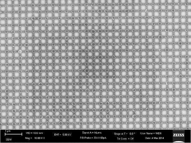
29 Czochralski method Single Crystal Silicon The crystal growth process is that a solid seed crystal is rotated and slowly extracted from a pool of molten silicon.
 Extremely little impurities. (< 0.")
30 Czochralski method Principle & Process: crystal growth method to obtain semiconductors (e.g. Si, Ge, GaAs) and metals (e.g. Pd, Pt, Ag, Au) Characteristics Rod-shaped single crystal is obtained from a melt of the same composition of melt. Very large crystal is obtained at once (e.g. 50 kg silicon rod with the size of ~2 m and width of 30 cm) Extremely little impurities. (< 0.01 ppb) Drawback: materials with high vapor pressure cannot be grown. Usages & Applications Production of highly pure semiconductors, metals, salts, and gemstones. Mass production of silicon wafers. Dopants can be added to make p-type or n-type semiconductors.

31 Bridgman-Stockbarger Technique Principle & Process: Heating polycrystalline material above its melting point and slowly cooling it from one end of its container, where a seed crystal is located. Stockbarger method: a pulling method like Czochralski method, boat pulled out through temperature gradient. Bridgman method: Melt is inside a temperature gradient furnace. Characteristics The shape of the crystal is defined by the container Drawback: materials is constantly in contact with sample boat, which introduces mechanical stress that possibly changes ideal crystal structure. Usages & Applications Page 31 Simple and popular way to producing semiconductor crystals GaAs, InP, and CdTe.

32 Zone Melting Method Principle & Process: Method for purifying crystals: impurities concentrate in the melt, and move to one end of container. Molten zone melts impure solid at its forward edge, and purer material is solidified behind it. Characteristics Pure solid can be obtained in a sample manner. Drawback: materials with high vapor pressure cannot be grown. Usages & Applications Page 32 Preparing high purity semiconductors for manufacturing transistors.

33 Flame Fusion Method (Verneuil Method) Principle & Process: Precursor pass through flame and then melted into liquid. Melted droplets fall on surface and crystal grows on it. Characteristics Rod-shaped gemstone crystal is obtained Useful for materials with high melting points. Drawback: excess oxygen induces gas bubble which includes imperfection of solids. Usages & Applications Growing crystals of metal oxides with high melting points, such as gemstones (ruby, sapphire). Page 33

34 Epitaxial Growth Epitaxy refers to the method of depositing a monocrystalline film on a monocrystalline (single crystal) substrate. The deposited film is denoted as epitaxial film or epitaxial layer. The term epitaxy comes from the Greek roots epi, meaning "above", and taxis, meaning "in ordered manner". It can be translated "to arrange upon" Page 34
. The most important aspect of MBE is the slow deposition rate (typically less than 1000 nm per hour),")

35 Molecular Beam Epitaxy (MBE) Molecular beam epitaxy takes place in high vacuum or ultra high vacuum (10 8 Pa). The most important aspect of MBE is the slow deposition rate (typically less than 1000 nm per hour), which allows the films to grow epitaxially. The slow deposition rates require better vacuum to achieve the same impurity levels as other deposition techniques. Page 35

36 Band gap engineering by Epitaxy Repeating a crystalline structure by: atom by atom addition. Chemistry controls the epitaxy to insure that, Ga bonds only to N and not Ga-Ga or N-N bonds Page 36

37 Metalorganic Vapor Phase Exitaxy For epitaxy of materials and compound semiconductors: combinations of Group III and Group V, Group II and Group VI, Group IV, or Group IV, V and VI elements Page 37
, phosphides (GaP,")
38 Atomic Layer Deposition (ALD) technique Amorphous film Metallic oxides, metallic nitrides, sulfides (ZnS, CdS), phosphides (GaP, InP),
 Templates Configuration diagram of the PAMs Interesting")
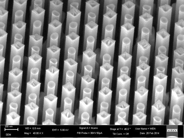
 Length <100 nm to >100")
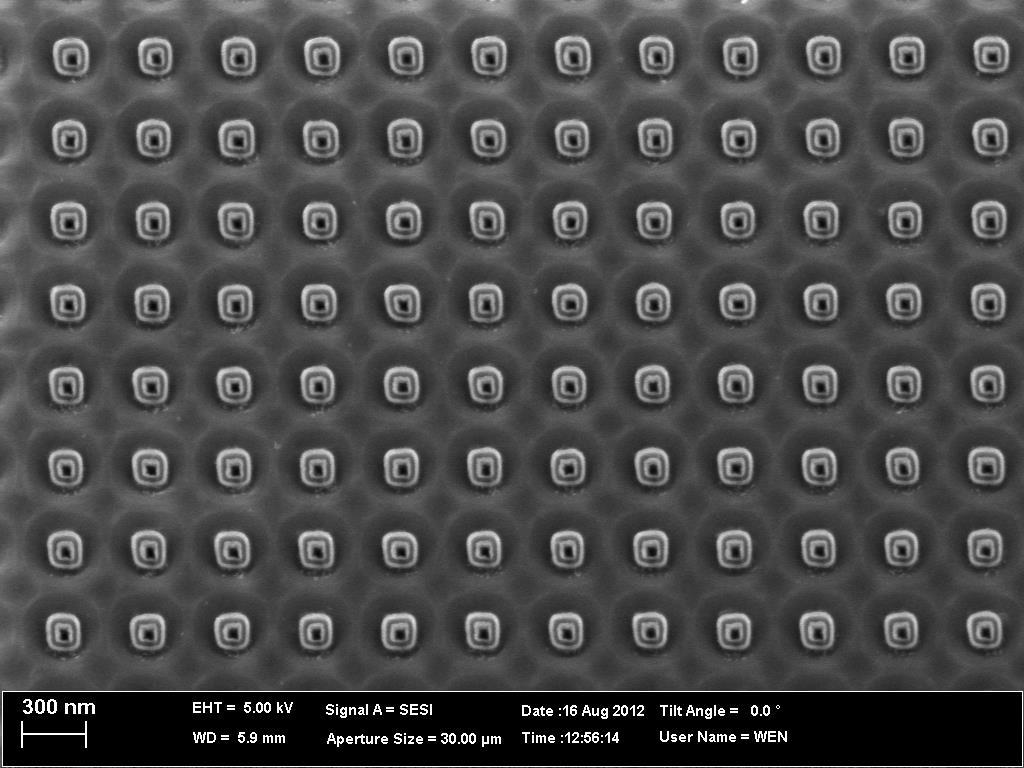
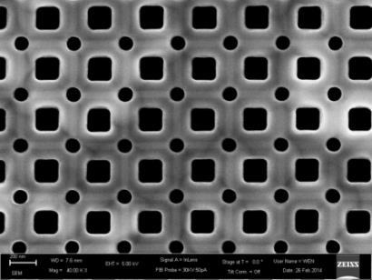
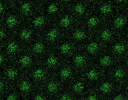
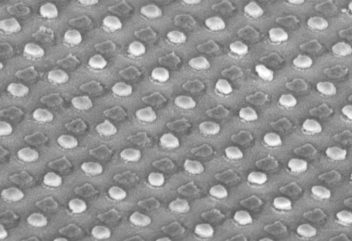
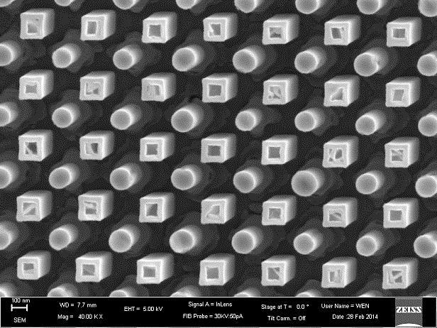
39 Template-based techniques to prepare functional nanostructures Porous Anodic Aluminum Oxide (AAO) Templates Configuration diagram of the PAMs Interesting and useful features: Ordered pore arrays + large area Nanometer-sized pores High aspect ratio Controllable diameter ( nm) Length <100 nm to >100 μm


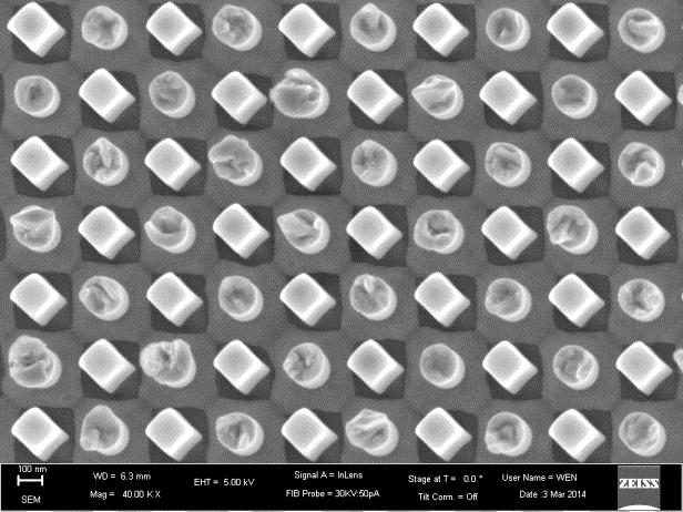
40 Templates with large-scale (1 mm 2 ) perfect rectangular pore arrays without defect 2010


41 Templates with large-scale (1 mm 2 ) perfect rectangle pore arrays without defect


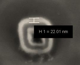
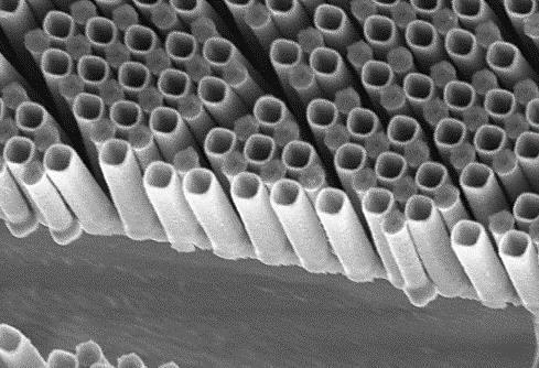
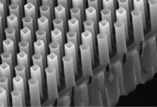
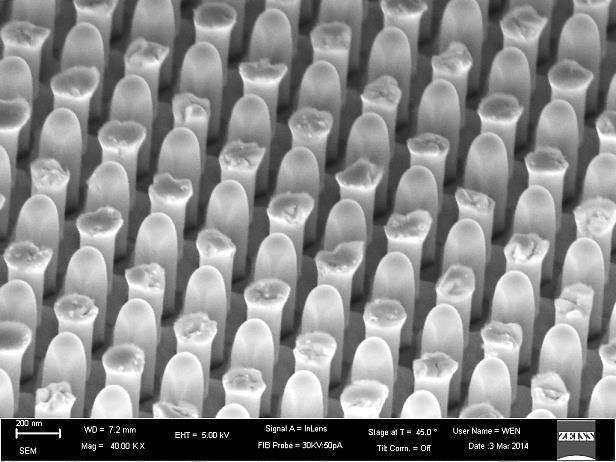
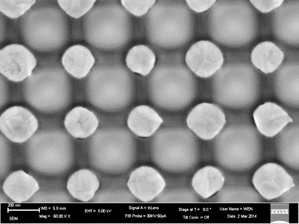
42 TiO 2 nanotubes grown in the template (Before removing template)
43


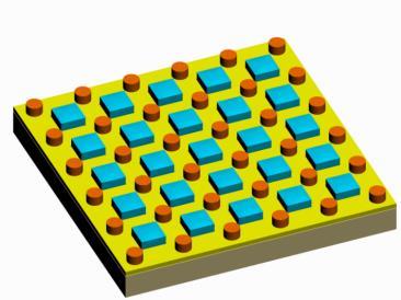
44 Sb Ni Ni-TiO 2 L. Liang, Y. Lei, et al. Energy & Environmental Science, 2015, 8, 2954; Y. Xu, Y. Lei, et al. Chemistry of Materials, 2015, 27, 4274.

45 Page 45 A B


 S K")


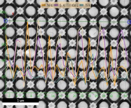
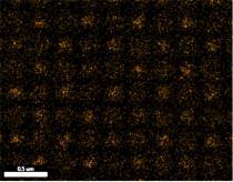
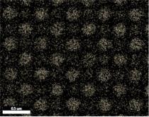
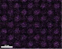
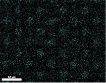
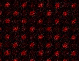
46 (a) (e) 200 nm 200 nm (b) Ni Ag C o Al P Ag Ni L Ag L 200 nm 200 nm (c) (f) 200 nm 200 nm (d) S K Cd L Ni L Ti K Page nm 200 nm


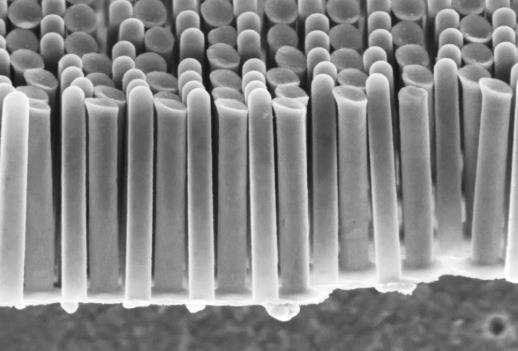
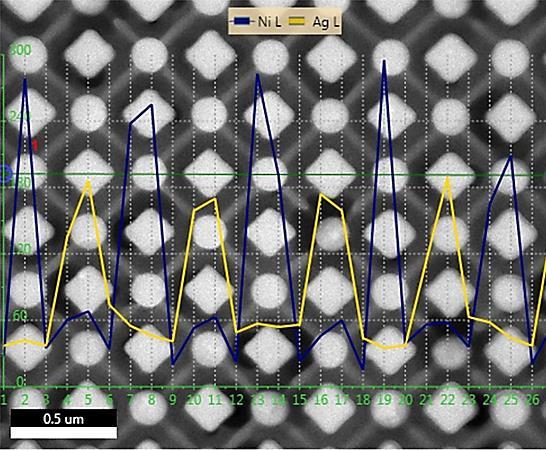
47 Binary nanowire arrays realized by electrodeposition via template TiO2/Ag TiO2/Au TiO2/Ni
48 Halbleiter Thank you!!! Prof. Yong Lei Prof. Thomas Hannappel
Lecture 1. Introduction to Electronic Materials. Reading: Pierret 1.1, 1.2, 1.4,
 Lecture 1 Introduction to Electronic Materials Reading: Pierret 1.1, 1.2, 1.4, 2.1-2.6 Atoms to Operational Amplifiers The goal of this course is to teach the fundamentals of non-linear circuit elements
Semiconductor Physics and Devices
 Syllabus Advanced Nano Materials Semiconductor Physics and Devices Textbook Donald A. Neamen (McGraw-Hill) Semiconductor Physics and Devices Seong Jun Kang Department of Advanced Materials Engineering
ELECTRONIC DEVICES AND CIRCUITS SUMMARY
 ELECTRONIC DEVICES AND CIRCUITS SUMMARY Classification of Materials: Insulator: An insulator is a material that offers a very low level (or negligible) of conductivity when voltage is applied. Eg: Paper,
Electron Energy, E E = 0. Free electron. 3s Band 2p Band Overlapping energy bands. 3p 3s 2p 2s. 2s Band. Electrons. 1s ATOM SOLID.
 Electron Energy, E Free electron Vacuum level 3p 3s 2p 2s 2s Band 3s Band 2p Band Overlapping energy bands Electrons E = 0 1s ATOM 1s SOLID In a metal the various energy bands overlap to give a single
Atoms? All matters on earth made of atoms (made up of elements or combination of elements).
.") Chapter 1 Atoms? All matters on earth made of atoms (made up of elements or combination of elements). Atomic Structure Atom is the smallest particle of an element that can exist in a stable or independent
Chapter 1 Atoms? All matters on earth made of atoms (made up of elements or combination of elements). Atomic Structure Atom is the smallest particle of an element that can exist in a stable or independent
Semiconductors. Semiconductors also can collect and generate photons, so they are important in optoelectronic or photonic applications.
 Semiconductors Semiconducting materials have electrical properties that fall between true conductors, (like metals) which are always highly conducting and insulators (like glass or plastic or common ceramics)
EE143 Fall 2016 Microfabrication Technologies. Evolution of Devices
 EE143 Fall 2016 Microfabrication Technologies Prof. Ming C. Wu wu@eecs.berkeley.edu 511 Sutardja Dai Hall (SDH) 1-1 Evolution of Devices Yesterday s Transistor (1947) Today s Transistor (2006) 1-2 1 Why
Conductivity and Semi-Conductors
 Conductivity and Semi-Conductors J = current density = I/A E = Electric field intensity = V/l where l is the distance between two points Metals: Semiconductors: Many Polymers and Glasses 1 Electrical Conduction
OPTI510R: Photonics. Khanh Kieu College of Optical Sciences, University of Arizona Meinel building R.626
 OPTI510R: Photonics Khanh Kieu College of Optical Sciences, University of Arizona kkieu@optics.arizona.edu Meinel building R.626 Announcements HW#3 is assigned due Feb. 20 st Mid-term exam Feb 27, 2PM
A semiconductor is an almost insulating material, in which by contamination (doping) positive or negative charge carriers can be introduced.
 positive or negative charge carriers can be introduced.") Semiconductor A semiconductor is an almost insulating material, in which by contamination (doping) positive or negative charge carriers can be introduced. Page 2 Semiconductor materials Page 3 Energy levels
Semiconductor A semiconductor is an almost insulating material, in which by contamination (doping) positive or negative charge carriers can be introduced. Page 2 Semiconductor materials Page 3 Energy levels
ELECTRONIC I Lecture 1 Introduction to semiconductor. By Asst. Prof Dr. Jassim K. Hmood
 ELECTRONIC I Lecture 1 Introduction to semiconductor By Asst. Prof Dr. Jassim K. Hmood SOLID-STATE ELECTRONIC MATERIALS Electronic materials generally can be divided into three categories: insulators,
Introduction to Semiconductor Physics. Prof.P. Ravindran, Department of Physics, Central University of Tamil Nadu, India
 Introduction to Semiconductor Physics 1 Prof.P. Ravindran, Department of Physics, Central University of Tamil Nadu, India http://folk.uio.no/ravi/cmp2013 Review of Semiconductor Physics Semiconductor fundamentals
EE 446/646 Photovoltaic Devices I. Y. Baghzouz
 EE 446/646 Photovoltaic Devices I Y. Baghzouz What is Photovoltaics? First used in about 1890, the word has two parts: photo, derived from the Greek word for light, volt, relating to electricity pioneer
Unit IV Semiconductors Engineering Physics
 Introduction A semiconductor is a material that has a resistivity lies between that of a conductor and an insulator. The conductivity of a semiconductor material can be varied under an external electrical
Semiconductors and Optoelectronics. Today Semiconductors Acoustics. Tomorrow Come to CH325 Exercises Tours
 Semiconductors and Optoelectronics Advanced Physics Lab, PHYS 3600 Don Heiman, Northeastern University, 2017 Today Semiconductors Acoustics Tomorrow Come to CH325 Exercises Tours Semiconductors and Optoelectronics
Chapter 1 Overview of Semiconductor Materials and Physics
 Chapter 1 Overview of Semiconductor Materials and Physics Professor Paul K. Chu Conductivity / Resistivity of Insulators, Semiconductors, and Conductors Semiconductor Elements Period II III IV V VI 2 B
Electro - Principles I
 Electro - Principles I Page 10-1 Atomic Theory It is necessary to know what goes on at the atomic level of a semiconductor so the characteristics of the semiconductor can be understood. In many cases a
From Last Time Important new Quantum Mechanical Concepts. Atoms and Molecules. Today. Symmetry. Simple molecules.
 Today From Last Time Important new Quantum Mechanical Concepts Indistinguishability: Symmetries of the wavefunction: Symmetric and Antisymmetric Pauli exclusion principle: only one fermion per state Spin
electronics fundamentals
 electronics fundamentals circuits, devices, and applications THOMAS L. FLOYD DAVID M. BUCHLA Lesson 1: Diodes and Applications Semiconductors Figure 1-1 The Bohr model of an atom showing electrons in orbits
Engineering 2000 Chapter 8 Semiconductors. ENG2000: R.I. Hornsey Semi: 1
 Engineering 2000 Chapter 8 Semiconductors ENG2000: R.I. Hornsey Semi: 1 Overview We need to know the electrical properties of Si To do this, we must also draw on some of the physical properties and we
Semiconductor Theory and Devices
 Semiconductor Theory and Devices Band Theory of Solids Semiconductor Theory Semiconductor Devices Nanotechnology It is evident that many years of research by a great many people, both before and after
EECS143 Microfabrication Technology
 EECS143 Microfabrication Technology Professor Ali Javey Introduction to Materials Lecture 1 Evolution of Devices Yesterday s Transistor (1947) Today s Transistor (2006) Why Semiconductors? Conductors e.g
Ch. 2: Energy Bands And Charge Carriers In Semiconductors
 Ch. 2: Energy Bands And Charge Carriers In Semiconductors Discrete energy levels arise from balance of attraction force between electrons and nucleus and repulsion force between electrons each electron
Review of Semiconductor Fundamentals
 ECE 541/ME 541 Microelectronic Fabrication Techniques Review of Semiconductor Fundamentals Zheng Yang (ERF 3017, email: yangzhen@uic.edu) Page 1 Semiconductor A semiconductor is an almost insulating material,
EE301 Electronics I , Fall
 EE301 Electronics I 2018-2019, Fall 1. Introduction to Microelectronics (1 Week/3 Hrs.) Introduction, Historical Background, Basic Consepts 2. Rewiev of Semiconductors (1 Week/3 Hrs.) Semiconductor materials
1 Review of semiconductor materials and physics
 Part One Devices 1 Review of semiconductor materials and physics 1.1 Executive summary Semiconductor devices are fabricated using specific materials that offer the desired physical properties. There are
Semiconductor Device Physics
 1 Semiconductor Device Physics Lecture 1 http://zitompul.wordpress.com 2 0 1 3 2 Semiconductor Device Physics Textbook: Semiconductor Device Fundamentals, Robert F. Pierret, International Edition, Addison
ISSUES TO ADDRESS...
 Chapter 12: Electrical Properties School of Mechanical Engineering Choi, Hae-Jin Materials Science - Prof. Choi, Hae-Jin Chapter 12-1 ISSUES TO ADDRESS... How are electrical conductance and resistance
Mat E 272 Lecture 25: Electrical properties of materials
 Mat E 272 Lecture 25: Electrical properties of materials December 6, 2001 Introduction: Calcium and copper are both metals; Ca has a valence of +2 (2 electrons per atom) while Cu has a valence of +1 (1
Lecture 2. Semiconductor Physics. Sunday 4/10/2015 Semiconductor Physics 1-1
 Lecture 2 Semiconductor Physics Sunday 4/10/2015 Semiconductor Physics 1-1 Outline Intrinsic bond model: electrons and holes Charge carrier generation and recombination Intrinsic semiconductor Doping:
Semiconductors 1. Explain different types of semiconductors in detail with necessary bond diagrams. Intrinsic semiconductors:
 Semiconductors 1. Explain different types of semiconductors in detail with necessary bond diagrams. There are two types of semi conductors. 1. Intrinsic semiconductors 2. Extrinsic semiconductors Intrinsic
Chapter Two. Energy Bands and Effective Mass
 Chapter Two Energy Bands and Effective Mass Energy Bands Formation At Low Temperature At Room Temperature Valence Band Insulators Metals Effective Mass Energy-Momentum Diagrams Direct and Indirect Semiconduction
Electronic Devices And Circuits. Introduction
 Electronic Devices And Circuits Introduction An electronic device controls the movement of electrons. The study of electronic devices requires a basic understanding of the relationship between electrons
Semiconductor Physics and Devices Chapter 3.
 Introduction to the Quantum Theory of Solids We applied quantum mechanics and Schrödinger s equation to determine the behavior of electrons in a potential. Important findings Semiconductor Physics and
3.1 Introduction to Semiconductors. Y. Baghzouz ECE Department UNLV
 3.1 Introduction to Semiconductors Y. Baghzouz ECE Department UNLV Introduction In this lecture, we will cover the basic aspects of semiconductor materials, and the physical mechanisms which are at the
Introduction to Engineering Materials ENGR2000. Dr.Coates
 Introduction to Engineering Materials ENGR2000 Chapter 18: Electrical Properties Dr.Coates 18.2 Ohm s Law V = IR where R is the resistance of the material, V is the voltage and I is the current. l R A
From Last Time. Several important conceptual aspects of quantum mechanics Indistinguishability. Symmetry
 From Last Time Several important conceptual aspects of quantum mechanics Indistinguishability particles are absolutely identical Leads to Pauli exclusion principle (one Fermion / quantum state). Symmetry
CME 300 Properties of Materials. ANSWERS: Homework 9 November 26, As atoms approach each other in the solid state the quantized energy states:
 CME 300 Properties of Materials ANSWERS: Homework 9 November 26, 2011 As atoms approach each other in the solid state the quantized energy states: are split. This splitting is associated with the wave
SEMICONDUCTOR PHYSICS
 SEMICONDUCTOR PHYSICS by Dibyendu Chowdhury Semiconductors The materials whose electrical conductivity lies between those of conductors and insulators, are known as semiconductors. Silicon Germanium Cadmium
Resistance (R) Temperature (T)
 Temperature (T)") CHAPTER 1 Physical Properties of Elements and Semiconductors 1.1 Introduction Semiconductors constitute a large class of substances which have resistivities lying between those of insulators and conductors.
CHAPTER 1 Physical Properties of Elements and Semiconductors 1.1 Introduction Semiconductors constitute a large class of substances which have resistivities lying between those of insulators and conductors.
Advantages / Disadvantages of semiconductor detectors
 Advantages / Disadvantages of semiconductor detectors Semiconductor detectors have a high density (compared to gas detector) large energy loss in a short distance diffusion effect is smaller than in gas
Nanostructures. Lecture 13 OUTLINE
 Nanostructures MTX9100 Nanomaterials Lecture 13 OUTLINE -What is quantum confinement? - How can zero-dimensional materials be used? -What are one dimensional structures? -Why does graphene attract so much
Calculating Band Structure
 Calculating Band Structure Nearly free electron Assume plane wave solution for electrons Weak potential V(x) Brillouin zone edge Tight binding method Electrons in local atomic states (bound states) Interatomic
LN 3 IDLE MIND SOLUTIONS
 IDLE MIND SOLUTIONS 1. Let us first look in most general terms at the optical properties of solids with band gaps (E g ) of less than 4 ev, semiconductors by definition. The band gap energy (E g ) can
EE495/695 Introduction to Semiconductors I. Y. Baghzouz ECE Department UNLV
 EE495/695 Introduction to Semiconductors I Y. Baghzouz ECE Department UNLV Introduction Solar cells have always been aligned closely with other electronic devices. We will cover the basic aspects of semiconductor
Modern Physics for Scientists and Engineers International Edition, 4th Edition
 Modern Physics for Scientists and Engineers International Edition, 4th Edition http://optics.hanyang.ac.kr/~shsong 1. THE BIRTH OF MODERN PHYSICS 2. SPECIAL THEORY OF RELATIVITY 3. THE EXPERIMENTAL BASIS
12/10/09. Chapter 18: Electrical Properties. View of an Integrated Circuit. Electrical Conduction ISSUES TO ADDRESS...
 Chapter 18: Electrical Properties ISSUES TO ADDRESS... How are electrical conductance and resistance characterized? What are the physical phenomena that distinguish? For metals, how is affected by and
Lecture 2 Electrons and Holes in Semiconductors
 EE 471: Transport Phenomena in Solid State Devices Spring 2018 Lecture 2 Electrons and Holes in Semiconductors Bryan Ackland Department of Electrical and Computer Engineering Stevens Institute of Technology
Misan University College of Engineering Electrical Engineering Department. Exam: Final semester Date: 17/6/2017
 Misan University College of Engineering Electrical Engineering Department Subject: Electronic I Class: 1 st stage Exam: Final semester Date: 17/6/2017 Examiner: Dr. Baqer. O. TH. Time: 3 hr. Note: Answer
2D MBE Activities in Sheffield. I. Farrer, J. Heffernan Electronic and Electrical Engineering The University of Sheffield
 2D MBE Activities in Sheffield I. Farrer, J. Heffernan Electronic and Electrical Engineering The University of Sheffield Outline Motivation Van der Waals crystals The Transition Metal Di-Chalcogenides
From nanophysics research labs to cell phones. Dr. András Halbritter Department of Physics associate professor
 From nanophysics research labs to cell phones Dr. András Halbritter Department of Physics associate professor Curriculum Vitae Birth: 1976. High-school graduation: 1994. Master degree: 1999. PhD: 2003.
Crystal Properties. MS415 Lec. 2. High performance, high current. ZnO. GaN
 Crystal Properties Crystal Lattices: Periodic arrangement of atoms Repeated unit cells (solid-state) Stuffing atoms into unit cells Determine mechanical & electrical properties High performance, high current
Chemistry Instrumental Analysis Lecture 8. Chem 4631
 Chemistry 4631 Instrumental Analysis Lecture 8 UV to IR Components of Optical Basic components of spectroscopic instruments: stable source of radiant energy transparent container to hold sample device
Semiconductor Nanowires: Motivation
 Semiconductor Nanowires: Motivation Patterning into sub 50 nm range is difficult with optical lithography. Self-organized growth of nanowires enables 2D confinement of carriers with large splitting of
Ga and P Atoms to Covalent Solid GaP
 Ga and P Atoms to Covalent Solid GaP Band Gaps in Binary Group III-V Semiconductors Mixed Semiconductors Affect of replacing some of the As with P in GaAs Band Gap (ev) (nm) GaAs 1.35 919 (IR) GaP 2.24
GaN based transistors
 GaN based transistors S FP FP dielectric G SiO 2 Al x Ga 1-x N barrier i-gan Buffer i-sic D Transistors "The Transistor was probably the most important invention of the 20th Century The American Institute
Chem 481 Lecture Material 3/20/09
 Chem 481 Lecture Material 3/20/09 Radiation Detection and Measurement Semiconductor Detectors The electrons in a sample of silicon are each bound to specific silicon atoms (occupy the valence band). If
Lecture 3b. Bonding Model and Dopants. Reading: (Cont d) Notes and Anderson 2 sections
 Notes and Anderson 2 sections") Lecture 3b Bonding Model and Dopants Reading: (Cont d) Notes and Anderson 2 sections 2.3-2.7 The need for more control over carrier concentration Without help the total number of carriers (electrons and
Lecture 3b Bonding Model and Dopants Reading: (Cont d) Notes and Anderson 2 sections 2.3-2.7 The need for more control over carrier concentration Without help the total number of carriers (electrons and
Chapter 4: Bonding in Solids and Electronic Properties. Free electron theory
 Chapter 4: Bonding in Solids and Electronic Properties Free electron theory Consider free electrons in a metal an electron gas. regards a metal as a box in which electrons are free to move. assumes nuclei
Free Electron Model for Metals
 Free Electron Model for Metals Metals are very good at conducting both heat and electricity. A lattice of in a sea of electrons shared between all nuclei (moving freely between them): This is referred
Contents CONTENTS. Page 2 of 47
 J. A. Hargreaves Lockerbie Academy June 2015 Contents CONTENTS Contents... 2 CHAPTER 7 CONDUCTORS, SEMICONDUCTORS AND INSULATORS... 4 Summary of Content... 4 Summary of this chapter- notes from column
Electronics The basics of semiconductor physics
 Electronics The basics of semiconductor physics Prof. Márta Rencz, Gergely Nagy BME DED September 16, 2013 The basic properties of semiconductors Semiconductors conductance is between that of conductors
Review of Semiconductor Physics. Lecture 3 4 Dr. Tayab Din Memon
 Review of Semiconductor Physics Lecture 3 4 Dr. Tayab Din Memon 1 Electronic Materials The goal of electronic materials is to generate and control the flow of an electrical current. Electronic materials
Semiconductor-Detectors
 Semiconductor-Detectors 1 Motivation ~ 195: Discovery that pn-- junctions can be used to detect particles. Semiconductor detectors used for energy measurements ( Germanium) Since ~ 3 years: Semiconductor
CHAPTER 2: ENERGY BANDS & CARRIER CONCENTRATION IN THERMAL EQUILIBRIUM. M.N.A. Halif & S.N. Sabki
 CHAPTER 2: ENERGY BANDS & CARRIER CONCENTRATION IN THERMAL EQUILIBRIUM OUTLINE 2.1 INTRODUCTION: 2.1.1 Semiconductor Materials 2.1.2 Basic Crystal Structure 2.1.3 Basic Crystal Growth technique 2.1.4 Valence
Electronic Properties of Lead Telluride Quantum Wells
 Electronic Properties of Lead Telluride Quantum Wells Liza Mulder Smith College 2013 NSF/REU Program Physics Department, University of Notre Dame Advisors: Profs. Jacek Furdyna, Malgorzata Dobrowolska,
Electrons are shared in covalent bonds between atoms of Si. A bound electron has the lowest energy state.
 Photovoltaics Basic Steps the generation of light-generated carriers; the collection of the light-generated carriers to generate a current; the generation of a large voltage across the solar cell; and
Introduction to Electronics and Semiconductor
 Introduction to Electronics and Semiconductor 1 Chapter Objectives To study and understand basic electronics. To study and understand semiconductor principles. 2 Definition Electronics is the branch of
For their 1948 discovery of the transistor, John Bardeen, Walter Brattain, and William Shockley were awarded the 1956 Nobel prize in physics.
 Modern Physics (PHY 3305) Lecture Notes Modern Physics (PHY 3305) Lecture Notes Solid-State Physics: Superconductivity (Ch. 10.9) SteveSekula, 1 April 2010 (created 1 April 2010) Review no tags We applied
Lecture 9: Metal-semiconductor junctions
 Lecture 9: Metal-semiconductor junctions Contents 1 Introduction 1 2 Metal-metal junction 1 2.1 Thermocouples.......................... 2 3 Schottky junctions 4 3.1 Forward bias............................
3C3 Analogue Circuits
 Department of Electronic & Electrical Engineering Trinity College Dublin, 2014 3C3 Analogue Circuits Prof J K Vij jvij@tcd.ie Lecture 1: Introduction/ Semiconductors & Doping 1 Course Outline (subject
KATIHAL FİZİĞİ MNT-510
 KATIHAL FİZİĞİ MNT-510 YARIİLETKENLER Kaynaklar: Katıhal Fiziği, Prof. Dr. Mustafa Dikici, Seçkin Yayıncılık Katıhal Fiziği, Şakir Aydoğan, Nobel Yayıncılık, Physics for Computer Science Students: With
Lecture 1. OUTLINE Basic Semiconductor Physics. Reading: Chapter 2.1. Semiconductors Intrinsic (undoped) silicon Doping Carrier concentrations
 silicon Doping Carrier concentrations") Lecture 1 OUTLINE Basic Semiconductor Physics Semiconductors Intrinsic (undoped) silicon Doping Carrier concentrations Reading: Chapter 2.1 EE105 Fall 2007 Lecture 1, Slide 1 What is a Semiconductor? Low
Lecture 1 OUTLINE Basic Semiconductor Physics Semiconductors Intrinsic (undoped) silicon Doping Carrier concentrations Reading: Chapter 2.1 EE105 Fall 2007 Lecture 1, Slide 1 What is a Semiconductor? Low
OPTI510R: Photonics. Khanh Kieu College of Optical Sciences, University of Arizona Meinel building R.626
 OPTI510R: Photonics Khanh Kieu College of Optical Sciences, University of Arizona kkieu@optics.arizona.edu Meinel building R.626 Announcements HW #6 is assigned, due April 23 rd Final exam May 2 Semiconductor
smal band gap Saturday, April 9, 2011
 small band gap upper (conduction) band empty small gap valence band filled 2s 2p 2s 2p hybrid (s+p)band 2p no gap 2s (depend on the crystallographic orientation) extrinsic semiconductor semi-metal electron
ELEC311( 물리전자, Physical Electronics) Course Outlines:
 Course Outlines:") ELEC311( 물리전자, Physical Electronics) Course Outlines: by Professor Jung-Hee Lee Lecture notes are prepared with PPT and available before the class (http://abeek.knu.ac.kr). The topics in the notes are
ELEC311( 물리전자, Physical Electronics) Course Outlines: by Professor Jung-Hee Lee Lecture notes are prepared with PPT and available before the class (http://abeek.knu.ac.kr). The topics in the notes are
CHAPTER 11 Semiconductor Theory and Devices
 CHAPTER 11 Semiconductor Theory and Devices 11.1 Band Theory of Solids 11.2 Semiconductor Theory 11.3 Semiconductor Devices 11.4 Nanotechnology It is evident that many years of research by a great many
Lecture 7: Extrinsic semiconductors - Fermi level
 Lecture 7: Extrinsic semiconductors - Fermi level Contents 1 Dopant materials 1 2 E F in extrinsic semiconductors 5 3 Temperature dependence of carrier concentration 6 3.1 Low temperature regime (T < T
Self-study problems and questions Processing and Device Technology, FFF110/FYSD13
 Self-study problems and questions Processing and Device Technology, FFF110/FYSD13 Version 2016_01 In addition to the problems discussed at the seminars and at the lectures, you can use this set of problems
Designing Information Devices and Systems II A. Sahai, J. Roychowdhury, K. Pister Discussion 1A
 EECS 16B Spring 2019 Designing Information Devices and Systems II A. Sahai, J. Roychowdhury, K. Pister Discussion 1A 1 Semiconductor Physics Generally, semiconductors are crystalline solids bonded into
EE 5211 Analog Integrated Circuit Design. Hua Tang Fall 2012
 EE 5211 Analog Integrated Circuit Design Hua Tang Fall 2012 Today s topic: 1. Introduction to Analog IC 2. IC Manufacturing (Chapter 2) Introduction What is Integrated Circuit (IC) vs discrete circuits?
EXTRINSIC SEMICONDUCTOR
 EXTRINSIC SEMICONDUCTOR In an extrinsic semiconducting material, the charge carriers originate from impurity atoms added to the original material is called impurity [or] extrinsic semiconductor. This Semiconductor
EE130: Integrated Circuit Devices
 EE130: Integrated Circuit Devices (online at http://webcast.berkeley.edu) Instructor: Prof. Tsu-Jae King (tking@eecs.berkeley.edu) TA s: Marie Eyoum (meyoum@eecs.berkeley.edu) Alvaro Padilla (apadilla@eecs.berkeley.edu)
First-Hand Investigation: Modeling of Semiconductors
 perform an investigation to model the behaviour of semiconductors, including the creation of a hole or positive charge on the atom that has lost the electron and the movement of electrons and holes in
Determination of properties in semiconductor materials by applying Matlab
 Determination of properties in semiconductor materials by applying Matlab Carlos Figueroa. 1, Raúl Riera A. 2 1 Departamento de Ingeniería Industrial. Universidad de Sonora A.P. 5-088, Hermosillo, Sonora.
Bohr s Model, Energy Bands, Electrons and Holes
 Dual Character of Material Particles Experimental physics before 1900 demonstrated that most of the physical phenomena can be explained by Newton's equation of motion of material particles or bodies and
* motif: a single or repeated design or color
 Chapter 2. Structure A. Electronic structure vs. Geometric structure B. Clean surface vs. Adsorbate covered surface (substrate + overlayer) C. Adsorbate structure - how are the adsorbed molecules bound
DO PHYSICS ONLINE ELECTRIC CURRENT FROM IDEAS TO IMPLEMENTATION ATOMS TO TRANSISTORS ELECTRICAL PROPERTIES OF SOLIDS
 DO PHYSICS ONLINE FROM IDEAS TO IMPLEMENTATION 9.4.3 ATOMS TO TRANSISTORS ELECTRICAL PROPERTIES OF SOLIDS ELECTRIC CURRENT Different substances vary considerably in their electrical properties. It is a
Free Electron Model for Metals
 Free Electron Model for Metals Metals are very good at conducting both heat and electricity. A lattice of in a sea of electrons shared between all nuclei (moving freely between them): This is referred
Graphene films on silicon carbide (SiC) wafers supplied by Nitride Crystals, Inc.
 wafers supplied by Nitride Crystals, Inc.") 9702 Gayton Road, Suite 320, Richmond, VA 23238, USA Phone: +1 (804) 709-6696 info@nitride-crystals.com www.nitride-crystals.com Graphene films on silicon carbide (SiC) wafers supplied by Nitride Crystals,
9702 Gayton Road, Suite 320, Richmond, VA 23238, USA Phone: +1 (804) 709-6696 info@nitride-crystals.com www.nitride-crystals.com Graphene films on silicon carbide (SiC) wafers supplied by Nitride Crystals,
UNIVERSITY OF CALIFORNIA College of Engineering Department of Electrical Engineering and Computer Sciences. Professor Ali Javey. Fall 2009.
 UNIVERSITY OF CALIFORNIA College of Engineering Department of Electrical Engineering and Computer Sciences EE143 Professor Ali Javey Fall 2009 Exam 1 Name: SID: Closed book. One sheet of notes is allowed.
Higher Physics. Electricity. Summary Notes. Monitoring and measuring a.c. Current, potential difference, power and resistance
 Higher Physics Electricity Summary Notes Monitoring and measuring a.c. Current, potential difference, power and resistance Electrical sources and internal resistance Capacitors Conductors, semiconductors
Electronic PRINCIPLES
 MALVINO & BATES Electronic PRINCIPLES SEVENTH EDITION Chapter 2 Semiconductors Topics Covered in Chapter 2 Conductors Semiconductors Silicon crystals Intrinsic semiconductors Two types of flow Doping a
Semiconductor physics I. The Crystal Structure of Solids
 Lecture 3 Semiconductor physics I The Crystal Structure of Solids 1 Semiconductor materials Types of solids Space lattices Atomic Bonding Imperfection and doping in SOLIDS 2 Semiconductor Semiconductors
So why is sodium a metal? Tungsten Half-filled 5d band & half-filled 6s band. Insulators. Interaction of metals with light?
 Bonding in Solids: Metals, Insulators, & CHEM 107 T. Hughbanks Delocalized bonding in Solids Think of a pure solid as a single, very large molecule. Use our bonding pictures to try to understand properties.
TFYA23 Crystal Growth Technology
 TFYA23 Crystal Growth Technology Course structure 10 double lectures 2 home assignments 2 laboratories Reporting Written report on the laboratories: SiC growth and characterization, week 49 Problem solutions,
EECS130 Integrated Circuit Devices
 EECS130 Integrated Circuit Devices Professor Ali Javey 8/30/2007 Semiconductor Fundamentals Lecture 2 Read: Chapters 1 and 2 Last Lecture: Energy Band Diagram Conduction band E c E g Band gap E v Valence
Semiconductor Polymer
 Semiconductor Polymer Organic Semiconductor for Flexible Electronics Introduction: An organic semiconductor is an organic compound that possesses similar properties to inorganic semiconductors with hole
ELEMENTARY BAND THEORY
 ELEMENTARY BAND THEORY PHYSICIST Solid state band Valence band, VB Conduction band, CB Fermi energy, E F Bloch orbital, delocalized n-doping p-doping Band gap, E g Direct band gap Indirect band gap Phonon
The first three categories are considered a bottom-up approach while lithography is a topdown
 Nanowires and Nanorods One-dimensional structures have been called in different ways: nanowires, nanorod, fibers of fibrils, whiskers, etc. The common characteristic of these structures is that all they