Introduction to Plasma Etching
|
|
|
- Ronald Reeves
- 6 years ago
- Views:
Transcription

1 Lam Research Corp. 1 Introduction to Plasma Etching Dr. Steve Sirard Technical Director Lam Research Corporation
2 Lam Research Corp. 2 Day 1 Review Plasma Fundamentals + e - e - + * e - + * + e - Collisional Processes -Ionization -Dissociation -Excitation + h Plasmas consists of electrons, ions, neutrals, radiation n e ~ n i << n g (weakly ionized) Collisional processes sustain the plasma and create radicals (etchant) Electrons are very hot Sheaths form at the walls/substrate to confine electrons and directionally accelerate ions


 + SiO 2")
 SiF 4 (g) + CO(g)")

3 Sheath ( V ~ V) Ion IED Flux Day 1 Review Anisotropic Plasma Etching Ion Energy (ev) Ion Energy (ev) + SiO 2 (s) + C x F y + I + (E i ) SiF 4 (g) + CO(g) Vertical, anisotropic etch Electrode Synergy! Lam Research Corp. 3
4 Lam Research Corp. 4 Day 2 - Outline Primary etching variables available to process engineers Common pattern transfer issues Advanced etch strategies: Pulsing strategies, Atomic layer etching Within-wafer etch uniformity control Plasma & surface diagnostics
5 What knobs are available to tune etch processes? Etching in general is very complex! Advanced plasma etch chambers are equipped with a lot of knobs for controlling the etch process Wafer temperature Upper electrode temperature Temperature gradients Chamber pressure Gas chemistry (~20 gases on a chamber to choose from) Gas ratios (gas partial pressures) Gas flow rate (residence time) Total RF power Multiple RF excitation frequencies (up to 3 generators) Pulsing of RF powers (duty cycle, frequency) Pulsing of gases (duty cycle, frequency) Etch time Multiple uniformity knobs Overall, a tremendously large process space long development cycles! Lam Research Corp. 5
6 Key etch variables: Gas Chemistry Etchant gases (e.g., CF 4, Cl 2, C 4 F 8 ) Provide reactants to etch materials of interest May provide polymer precursors for anisotropy, selectivity Oxidants (e.g., O 2 ) Used to increase etchant concentrations Suppress polymer formation Radical-Scavengers (e.g., H 2 ) Increase polymer formation, selectivity Reduce etchant concentration Inhibitor-Former (e.g., CH 3 F, CH 4 ) Induce anisotropy Improve selectivity Inert Gases (e.g., Ar, He) Dilute etchant Stabilize plasma Enhance anisotropy Improve heat transfer Lam Research Corp. 6
7 Ion Energy Lam Research Corp. 7 Key etch variables: Chamber Pressure Pressure directly influences major phenomena that control plasma etching Physical Sputtering 1. Energy of ions bombarding surfaces 2. Ion-to-neutral ratio/flux 3. Polymerization potential 4. Electron energies 5. Surface coverage by physisorption 6. Chemical kinetics 7. Relative rates of mass transport processes 8. Etch rate uniformity across wafer Ion-assisted etching Pressure (Torr) Chemical plasma etching

8 Lam Research Corp. 8 Key etch variables: RF Power/Frequency RF Power/Excitation Frequency can influence: 1. Spatial distributions of species across the plasma (Uniformity) 2. Ion energy distribution 3. Plasma density 4. Effects plasma chemistry For example, one frequency may promote polymer deposition, while another frequency may etch polymer 5. Selectivity


9 Lam Research Corp. 9 Key etch variables: Surface Temperatures Surface temperatures can effect: 1. Surface morphology 2. Polymer deposition 3. Selectivity 4. Resist flowing/wiggling/roughness 3-Frequency 5. Product volatility/etch rate 6. Temperature gradients Thermophoresis effects Selectivity/Uniformity impact T etch ~ T g T etch << T g
10 Common Pattern Transfer Issues Lam Research Corp. 10
11 Lam Research Corp. 11 Process Issues Loading Effects: Macro-loading Macro-loading Etch rate for a given process becomes slower with more exposed etch area Due to overall depletion of reactant with more exposed area to etch Examples of macro-loading issues in industry Process shift on two different wafers with same features but different etchable area Chamber etch rate drift due to build up of polymer on chamber parts during etch processing
12 Macro-loading Example: Depletion of reactant with larger exposed area PR etch rate (A/min) Lam Research Corp. 12 Photoresist etch with oxidizing plasma chemistry When exposed area of resist is large, etch rate is reduced everywhere, but even more so in the wafer center When exposed area of resist is small, etch rate is higher and more uniform Typical edge fast etch rate of resist is due to loading of plasma by large area of resist 3500 PR coupons Si PR coupons PR 500 PR coupons on PR wafer PR coupons on Si wafer Wafer position (mm)
13 Lam Research Corp. 13 Macro-loading Characteristics Etch rate is limited by the arrival of neutrals (neutral-limited regime) Macro-loading is a function of total exposed area reacting with gas phase species Center-to-edge uniformity variations can be a result of macro-loading Compensation Strategies General process fine-tuning and uniformity compensation Increase etchant flux to make less neutral-limited (e.g., pressure, gas ratio change, higher RF power to increase dissociation)

14 Lam Research Corp. 14 Loading effects: Micro-loading Macro-loading etch rate becomes slower due to overall depletion of reactant with more exposed etch area Micro-loading - etch difference between a given feature located in an area of high density compared to the same feature in an area of low density (isolated) on the same chip (assumes same nominal aspect ratio) Due to local depletion of reactant Isolated trench etches faster than dense area


15 Lam Research Corp. 15 Is Micro-loading real?? Unequal consumption across the chip results in lateral concentration gradients However, significant gradients may require 100s of microns at low pressures Compensation Lower pressure fewer collisions higher diffusion rate less micro-loading Increase etchant flux (e.g., Change gas ratio, increase source power)
 ARDE etch rate")

16 Lam Research Corp. 16 Aspect Ratio Dependent Etching (ARDE) ARDE etch rate becomes slower with higher aspect ratio or smaller critical dimensions Sometimes the phenomena is also called RIE Lag Aspect Ratio = Depth / Width
17 Lam Research Corp. 17 Primary ARDE Mechanisms Classical-ARDE: Higher aspect ratio features generally etch slower than smaller aspect ratio features Four primary mechanisms used to explain ARDE: 1. Neutral shadowing 2. Ion shadowing 3. Differential charging 4. Knudsen transport
18 Lam Research Corp. 18 ARDE Mechanisms: Neutral Shadowing The neutral angular distribution is isotropic Neutrals incident at a large angle to the normal will hit the top or sidewall of the feature, and can be lost (e.g., recombination) before reaching the bottom of the feature They will be shadowed by the walls of the feature Ion/neutral flux ratio is aspect ratio dependent due to different angular distributions High aspect ratio features may become starved for neutrals (ER slows down in HAR feature)
19 Lam Research Corp. 19 ARDE Mechanisms: Ion Shadowing The ion angular distribution is generally anisotropic Higher pressures can cause ion scattering in the sheath, causing spread in ion energies/angular distributions Ions incident at larger angles to the normal hit the top or sidewall of the feature, but not the bottom (i.e, they are shadowed) Similar to neutral shadowing, ion shadowing shifts the ion/neutral flux ratio in different AR features


20 Lam Research Corp. 20 ARDE Mechanisms: Differential Charging Electron flux to the wafer periodically occurs as the sheath oscillates, and has a much less anisotropic angular distribution Differential charging can result in potentials large enough to deflect ions (alters flux to feature bottom) Others have reported ion energy drops of ~30% for AR ~ 3

21 Lam Research Corp. 21 ARDE Mechanisms: Knudsen transport Knudsen transport Neutral reactants travel to the bottom of the feature by being reflected diffusively from the sidewalls without reacting From Coburn & Winters, APL, (1989) J b S b = J t (1- )J t (1-S b )J b (describes gas fluxes into and out of feature) J b, J t = flux to the bottom or top of feature S b = reaction probability at the bottom of the feature = transmission probability (decreases with increasing aspect ratio) Etch Rate Ratio (bottom/top) vs Aspect Ratio
?")
22 Lam Research Corp. 22 What about Inverse-ARDE (or Reverse-RIE Lag)? Classical ARDE Inverse ARDE
 Mechanism Polymer-precursor shadowing Less polymer forms in high aspect ratio")
23 Lam Research Corp. 23 Inverse-ARDE (or Reverse-RIE Lag) Mechanism Polymer-precursor shadowing Less polymer forms in high aspect ratio feature, thus higher etch rate Shadowing gives less polymer deposition here More polymer deposition here
24 Lam Research Corp. 24 How do we fix ARDE?? Multiple mechanisms can lead to ARDE in plasma etching Neutral shadowing Ion shadowing Differential charging Knudsen transport Solution to ARDE issues can depend on which mechanism(s) is/are responsible In previous dielectric etch study, we observed that differential charging was a primary mechanism for classical ARDE To mitigate, low pressures improve (as long as not too low neutral limited) Higher RF powers (higher ion energies) improve Balancing the etchant/deposition flux can also compensate (gas chemistry, gas ratios) RF pulsing/atomic layer etching improves Inverse-ARDE is related to shadowing of polymer precursors in narrow features Shift etch chemistry to less polymerizing condition (increase F/C ratio, add O 2, etc)


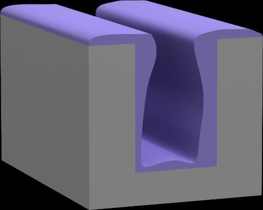
25 Lam Research Corp. 25 Other issues: Faceting and Necking Strasser, JVSTB, 2007 Lee, JECS, 2010 Faceting Generally due to increased yield per ion at a corner (Dependent on ion energy/flux) Necking Can be due to heavy polymer deposition at the top of the contact or from redeposition of polymer precursors, forward scattered from photoresist Position of neck may be dependent on the angle in the resist
26 Lam Research Corp. 26 Bowing Bowing of the feature sidewall can have several root causes Ion scattering from the resist mask (dependent on facet angle) Ion scattering in the sheath (lower pressure may help) Too much oxygen in the process (less sidewall polymer protection, leads to more isotropic etch) Exacerbated by polymers that deposit well at the top of features, but deposit poorly deeper down the feature


27 Lam Research Corp. 27 Microtrenching Clarycon Schaepkens, APL, (1998) Bogart, JVSTA, (2000) Microtrenching - Localized higher etch rate at bottom corners of trench Potential Mechanisms 1. Ion scattering from sloped trench sidewalls 2. Ion deflection due to differential charging of microstructures


28 Lam Research Corp. 28 Striations Extended roughness on the sidewalls of etched features Seen on both holes and trenches Due to roughness/striation formation in the resist being transferred to underlayers Exacerbated with 193nm resists Likely related to how plasma modifies the resists at different length scales Ions impact ~2nm of surface, causing graphitic-densified region VUV radiation may either chain scission or cross-link at deeper depths (~100nm) Different mechanical properties of modified layers can lead to resist buckling or roughening
29 Advanced Etch Strategies Lam Research Corp. 29
30 RF Pulsing Can Lower Ratio of High:Low Ion Energy Flux CW 2 MHz Bias CW 60 MHz Source Pulsing reduces the ratio of high to low energy ions (constant peak power) [G hi /G lo ] pulsed < [G hi /G lo ] cw Pulsed 2 MHz Bias CW 60 MHz Source RF pulsing can be used to access energy distributions not available in continuous operation RF pulsing can access new process regimes to break existing tradeoffs Lam Research Corp. 30

31 RF Pulsing Controls Neutral:Ion Flux Different decay time constants allows to vary Ion/Neutral flux over larger range Pulsing improves selectivity and controls ARDE Slide - 31 Lam Research Confidential
 High bias for increased etch rate,")
32 Lam Research Corp. 32 Bias pulsing can improve line edge roughness On just turned off Off Neutral Passivant Ion Ions sputter (can facet, lower selectivity, worse LER ) High bias for increased etch rate, less bow Passivants build-up, less LER, better selectivity Reactant still etching Neutrals saturated, reduces intracell loading repeat 3x Improvement on LER observed


33 Atomic Layer Etching How can we achieve a more precise etch?? Lam Research Corp. 33 Continuous Wave Plasma Processing 3 5 nm Time At the atomic scale, continuous plasmas surface precision degrades as we etch for longer times Ions are damaging surface Mixing occurring in the reaction layer (~3 5 nm thick)


34 Directional Atomic Layer Processing: The Penultimate Means of Reducing Variability Lam Research Corp. 34 Start Reaction A Switch Steps Reaction B End/Repeat Etch Ar+ Cl 2 Si Surface Si ALE Chlorination Ion Bombardment Deposition O Radical Si Source SiO 2 Added SiO 2 ALD Adsorption Adsorption Use separate, self-limiting steps for atomic layer removal


35 Avoid Use of Energetic Reactive Ions to Achieve Atomic Layer Precision ~3 nm ~0.5 nm Lam Research Corp. 35 Cl+ 50 ev Vs. Ar+ 50 ev Efficient in breaking bonds, creating more mixing and disorder Si Si Inert ions create disordered regions near surface and also recrystallize these regions Source: Humbird and Graves, 2004 Roughening effect, inhomogeneity Used in conventional etching: Smoothing effect Used in directional ALE schemes: 10 nm Source: 10 nm Si Lam, 2010 Si 1 nm Source: Agarwal & Kushner, 2007


 2.")
36 Lam Research Corp. 36 ALE Process Window Ion Energy too low Ideal Regime Excessive ion energy/bombardment Incomplete Removal ALE Window Sputtering 1. Saturate the surface with reactant (without ion bombardment) 2. Bombard surface with ions at the proper ion energy, in the absence of excess reactant


37 Lam Research Corp. 37 Profile benefits of using separated and self-limiting steps Conventional Deposition ALD Conventional Etch ALE


38 Other benefits from separated and self-limiting steps Lam Research Corp. 38


39 Lam Research Corp. 39 Atomic layer etch process Limitations But I am not afraid to consider the final question as to whether, ultimately---in the great future---we can arrange the atoms the way we want; the very atoms, all the way down! -Richard P. Feynman, Dec 29th 1959 at the annual meeting of American Physical Society Limitations from the process: Photon-induced etching and damage Ion-induced mixing and damage even with inert ions at low energies Steric hindrance preventing fully saturated coverage Adsorbed reactants on chamber walls compromise separation of dosing and activation steps Trade-off between atomic layer processing benefits and throughput ALD/ALE: Feynman s dream ALD/ALE: Penultimate reality
40 Etch Uniformity Control Lam Research Corp. 40
41 Lam Research Corp. 41 Etch uniformity control Leading edge wafer fabrication processes require very tight uniformity control across the wafer (Out to <3mm from the edge of the wafer; Require specs ~ <1 nm 3-sigma) Uniformity in etch depths Uniformity in critical dimensions Center-to-edge uniformity in plasma processes are difficult due to discontinuities that occur at the wafer edge Impact on local chemistry and ion flux Temperature gradients Plasma Wafer Advanced etch tools use a variety of compensation strategies to achieve uniformity across the wafer
42 Adjusting the gap distance between upper and lower electrodes tunes the plasma uniformity across the wafer Lam Research Corp. 42
43 For ion-limited etch regimes, etch rates can be flipped from center-fast to edge-fast by changing gap distance Pilot wafer measurement results CF 4 /Ar process 150 Ar/CF4 process 28 At wafer center Etch rate changes by ~2.1% Ion flux changes by ~2.2% TOX ER (nm/min.) Isat (ua) At wafer edge Etch rate changes by ~-8% gap 1.2 gap 0.85 gap Wafer radius (mm) Etch rate 24 Ion flux changes by ~-7% Isat (v3) Slide - 43 Lam Research Confidential
44 Gap changes can also impact etch uniformity of neutrallimited processes Lam Research Corp. 44
45 Effective Tuning Knobs for ER and CD Uniformity for In situ Mask + Dielectric Etching PR Typical Operation Mode ARC / Si-SOC Organic High gap (>1.07) + tuning gas TEM Low K Low gap (0.85) + tuning gas SiCN Medium gap (1.07) + tuning gas Sub-Si Enables all in one etching with optimized uniformity in each step (v3) Slide - 45 Lam Research Confidential
46 BARC(1.07gap)/ACL(1. 07)/PEOX(1.07) BARC(1.07gap)/ACL(0. 85)/PEOX(1.07) BARC(1.07gap)/ACL(0. 85)/PEOX(0.98) CD (nm) 3s (nm) Case study: Effect of gap and tuning gas on CD uniformity for in-situ mask + dielectric etching Case study: CD uniformity improvement with adjustable ACLgap and tuning gas Oxide Example: Line CD Uniformity Data on Patterned Wafers PR BARC SiON W BARC 1.07gap 1.07gap 1.07gap ACL 1.07gap 0.85gap 0.85gap OXIDE 1.07gap 1.07gap 0.98gap (v3) Slide - 46 While maintaining the average CD values, uniformity is improved by optimizing the gap height for each step. Lam Research Confidential


47 Increased temperature control across the wafer Lam Research Corp. 47

48 Multi-zone electrostatic chuck (ESC) temperature control allows precise etch rate tuning Lam Research Corp. 48
49 Plasma & Surface Diagnostics Lam Research Corp. 49
50 Lam Research Corp. 50 Plasma & Surface Diagnostics Because of the complexity of the chemical and physical environments in a plasma, a large array of techniques are required to characterize them Parameters that are of normal interest Electron and ion densities Neutral densities (both species created in the plasma and byproducts of etch process) Respective temperatures of these species Energy distributions Characterization of electric fields Surface modification Relative importance of different species within plasma
 is measured as a function of V. What can you measure?")
51 Lam Research Corp. 51 Plasma Diagnostics Langmuir Probe Conducting wire placed in the plasma with a variable bias, V, applied. The current (I) is measured as a function of V. What can you measure? Floating potential Plasma potential Plasma density Ion current density EEDF/Electron temperature
 examines photon emissions from the plasma Characteristic set of wavelengths emitted for a")
52 OES (arb. units) Plasma Diagnostics Residual Gas Analyzers uses mass spec to analyze gases present in vacuum environment What can you measure? Gas species analysis/leak detection Insight into reaction mechanisms Optical Emission Spectroscopy (OES) examines photon emissions from the plasma Characteristic set of wavelengths emitted for a given species What can you measure? Monitor species in the plasma End-pointing etch process Snapshot OES of N 2 /H 2 Plasma N2/H2 process Wavelength (nm) Lam Research Corp. 52


53 Lam Research Corp. 53 Plasma Diagnostics Optical Emissions OES continued Endpointing measure emission from a key species as a function of time to determine when to stop etch Troubleshoot chamber drifts Endpoint Detection Endpoint Endpoint Time Trend Charts Chamber excursion? Chamber drifting? Bad wafer?
54 Lam Research Corp. 54 Plasma Diagnostics Actinometry using OES add small/known amount of noble gas (e.g., Ar) to a reactive plasma and concurrently monitor the emissions of the noble gas and the reactive species (e.g., F). Infer densities of certain species (e.g., [F]) Many assumptions have to be met, so be careful Excited state emission energy of noble gas is similar to emission in reactive species Same group of electrons responsible for excitation of both levels Excitation efficiencies of these levels will have similar dependence on plasma parameters Absorption Spectroscopy use stable, well-defined light source to excite radicals from ground electronic state What can we measure? Measure absolute densities of plasma species
55 Lam Research Corp. 55 Plasma/Surface diagnostics Shaded structures Shaded structures structures or windows that are often placed on the substrate to shade or block out targeted species from the plasma What can be measured? Separate out the effects of radicals, radiation, and ions Impact of Radicals (block ions, radiation) Impact of Radicals, UV/VUV, and Radical+UV/VUV neutrals ions Si roof 0.6 mm gap Si wafer Measure neutral-driven deposition in ion-shaded region
56 Lam Research Corp. 56 Surface Diagnostics Spectroscopic ellipsometry Measure optical constants and film thickness Used ex-situ and in-situ to study plasma effects/kinetics IR absorption Provide chemical identification XPS Surface elemental analysis Chemical identification (bonding info, etc) Adsorbate coverage Spinning Wall (Donnelly group at UH) Elemental analysis and chemical identification (with proper diagnostic) Adsorbate coverages Recombination probabilities Plasmas causes a lot of damage to near surface region, so often will see significant oxidation when performing ex situ surface analysis

")

57 Lam Research Corp. 57 Check us out for career and internship opportunities! Bay Area, CA (Headquarters) Portland, OR Villach, Austria

58
ETCHING Chapter 10. Mask. Photoresist
 ETCHING Chapter 10 Mask Light Deposited Substrate Photoresist Etch mask deposition Photoresist application Exposure Development Etching Resist removal Etching of thin films and sometimes the silicon substrate
Plasma Chemistry Study in an Inductively Coupled Dielectric Etcher
 Plasma Chemistry Study in an Inductively Coupled Dielectric Etcher Chunshi Cui, John Trow, Ken Collins, Betty Tang, Luke Zhang, Steve Shannon, and Yan Ye Applied Materials, Inc. October 26, 2000 10/28/2008
Reactive Ion Etching (RIE)
") Reactive Ion Etching (RIE) RF 13.56 ~ MHz plasma Parallel-Plate Reactor wafers Sputtering Plasma generates (1) Ions (2) Activated neutrals Enhance chemical reaction 1 2 Remote Plasma Reactors Plasma Sources
Reactive Ion Etching (RIE) RF 13.56 ~ MHz plasma Parallel-Plate Reactor wafers Sputtering Plasma generates (1) Ions (2) Activated neutrals Enhance chemical reaction 1 2 Remote Plasma Reactors Plasma Sources
E SC 412 Nanotechnology: Materials, Infrastructure, and Safety Wook Jun Nam
 E SC 412 Nanotechnology: Materials, Infrastructure, and Safety Wook Jun Nam Lecture 10 Outline 1. Wet Etching/Vapor Phase Etching 2. Dry Etching DC/RF Plasma Plasma Reactors Materials/Gases Etching Parameters
CHAPTER 6: Etching. Chapter 6 1
 Chapter 6 1 CHAPTER 6: Etching Different etching processes are selected depending upon the particular material to be removed. As shown in Figure 6.1, wet chemical processes result in isotropic etching
Chapter 7 Plasma Basic
 Chapter 7 Plasma Basic Hong Xiao, Ph. D. hxiao89@hotmail.com www2.austin.cc.tx.us/hongxiao/book.htm Hong Xiao, Ph. D. www2.austin.cc.tx.us/hongxiao/book.htm 1 Objectives List at least three IC processes
Device Fabrication: Etch
 Device Fabrication: Etch 1 Objectives Upon finishing this course, you should able to: Familiar with etch terminology Compare wet and dry etch processes processing and list the main dry etch etchants Become
Etching: Basic Terminology
 Lecture 7 Etching Etching: Basic Terminology Introduction : Etching of thin films and sometimes the silicon substrate are very common process steps. Usually selectivity, and directionality are the first
Etching Issues - Anisotropy. Dry Etching. Dry Etching Overview. Etching Issues - Selectivity
 Etching Issues - Anisotropy Dry Etching Dr. Bruce K. Gale Fundamentals of Micromachining BIOEN 6421 EL EN 5221 and 6221 ME EN 5960 and 6960 Isotropic etchants etch at the same rate in every direction mask
Chapter 7. Plasma Basics
 Chapter 7 Plasma Basics 2006/4/12 1 Objectives List at least three IC processes using plasma Name three important collisions in plasma Describe mean free path Explain how plasma enhance etch and CVD processes
EE 527 MICROFABRICATION. Lecture 25 Tai-Chang Chen University of Washington
 EE 527 MICROFABRICATION Lecture 25 Tai-Chang Chen University of Washington ION MILLING SYSTEM Kaufmann source Use e-beam to strike plasma A magnetic field applied to increase ion density Drawback Low etch
Lecture 6 Plasmas. Chapters 10 &16 Wolf and Tauber. ECE611 / CHE611 Electronic Materials Processing Fall John Labram 1/68
 Lecture 6 Plasmas Chapters 10 &16 Wolf and Tauber 1/68 Announcements Homework: Homework will be returned to you on Thursday (12 th October). Solutions will be also posted online on Thursday (12 th October)
Lecture 11. Etching Techniques Reading: Chapter 11. ECE Dr. Alan Doolittle
 Lecture 11 Etching Techniques Reading: Chapter 11 Etching Techniques Characterized by: 1.) Etch rate (A/minute) 2.) Selectivity: S=etch rate material 1 / etch rate material 2 is said to have a selectivity
UNIT 3. By: Ajay Kumar Gautam Asst. Prof. Dev Bhoomi Institute of Technology & Engineering, Dehradun
 UNIT 3 By: Ajay Kumar Gautam Asst. Prof. Dev Bhoomi Institute of Technology & Engineering, Dehradun 1 Syllabus Lithography: photolithography and pattern transfer, Optical and non optical lithography, electron,
Section 3: Etching. Jaeger Chapter 2 Reader
 Section 3: Etching Jaeger Chapter 2 Reader Etch rate Etch Process - Figures of Merit Etch rate uniformity Selectivity Anisotropy d m Bias and anisotropy etching mask h f substrate d f d m substrate d f
Plasma Etching: Atomic Scale Surface Fidelity and 2D Materials
 1 Plasma Etching: Atomic Scale Surface Fidelity and 2D Materials Thorsten Lill, Keren J. Kanarik, Samantha Tan, Meihua Shen, Alex Yoon, Eric Hudson, Yang Pan, Jeffrey Marks, Vahid Vahedi, Richard A. Gottscho
4FNJDPOEVDUPS 'BCSJDBUJPO &UDI
 2010.5.4 1 Major Fabrication Steps in CMOS Process Flow UV light oxygen Silicon dioxide Silicon substrate Oxidation (Field oxide) photoresist Photoresist Coating Mask exposed photoresist Mask-Wafer Exposed
Wet and Dry Etching. Theory
 Wet and Dry Etching Theory 1. Introduction Etching techniques are commonly used in the fabrication processes of semiconductor devices to remove selected layers for the purposes of pattern transfer, wafer
Plasma Deposition (Overview) Lecture 1
 Lecture 1") Plasma Deposition (Overview) Lecture 1 Material Processes Plasma Processing Plasma-assisted Deposition Implantation Surface Modification Development of Plasma-based processing Microelectronics needs (fabrication
Plasma Deposition (Overview) Lecture 1 Material Processes Plasma Processing Plasma-assisted Deposition Implantation Surface Modification Development of Plasma-based processing Microelectronics needs (fabrication
LECTURE 5 SUMMARY OF KEY IDEAS
 LECTURE 5 SUMMARY OF KEY IDEAS Etching is a processing step following lithography: it transfers a circuit image from the photoresist to materials form which devices are made or to hard masking or sacrificial
EE 527 MICROFABRICATION. Lecture 24 Tai-Chang Chen University of Washington
 EE 527 MICROFABRICATION Lecture 24 Tai-Chang Chen University of Washington EDP ETCHING OF SILICON - 1 Ethylene Diamine Pyrocatechol Anisotropy: (100):(111) ~ 35:1 EDP is very corrosive, very carcinogenic,
Etching Applications and Discoveries Made Possible by Advanced Ion Energy Control
 Etching Applications and Discoveries Made Possible by Advanced Ion Energy Control Possible by Advanced Ion Energy Control V. M. Donnelly Department of Chemical and Biomolecular Engineering University of
EE C245 ME C218 Introduction to MEMS Design Fall 2007
 EE C245 ME C218 Introduction to MEMS Design Fall 2007 Prof. Clark T.-C. Nguyen Dept. of Electrical Engineering & Computer Sciences University of California at Berkeley Berkeley, CA 94720 Lecture 11: Bulk
DEPOSITION AND COMPOSITION OF POLYMER FILMS IN FLUOROCARBON PLASMAS*
 DEPOSITION AND COMPOSITION OF POLYMER FILMS IN FLUOROCARBON PLASMAS* Kapil Rajaraman and Mark J. Kushner 1406 W. Green St. Urbana, IL 61801 rajaramn@uiuc.edu mjk@uiuc.edu http://uigelz.ece.uiuc.edu November
MODELING OF SEASONING OF REACTORS: EFFECTS OF ION ENERGY DISTRIBUTIONS TO CHAMBER WALLS*
 MODELING OF SEASONING OF REACTORS: EFFECTS OF ION ENERGY DISTRIBUTIONS TO CHAMBER WALLS* Ankur Agarwal a) and Mark J. Kushner b) a) Department of Chemical and Biomolecular Engineering University of Illinois,
Plasma-Surface Interactions in Patterning High-k k Dielectric Materials
 Plasma-Surface Interactions in Patterning High-k k Dielectric Materials October 11, 4 Feature Level Compensation and Control Seminar Jane P. Chang Department of Chemical Engineering University of California,
PRINCIPLES OF PLASMA DISCHARGES AND MATERIALS PROCESSING
 PRINCIPLES OF PLASMA DISCHARGES AND MATERIALS PROCESSING Second Edition MICHAEL A. LIEBERMAN ALLAN J, LICHTENBERG WILEY- INTERSCIENCE A JOHN WILEY & SONS, INC PUBLICATION CONTENTS PREFACE xrrii PREFACE
The effect of the chamber wall on fluorocarbonassisted atomic layer etching of SiO 2 using cyclic Ar/C 4 F 8 plasma
 The effect of the chamber wall on fluorocarbonassisted atomic layer etching of SiO 2 using cyclic Ar/C 4 F 8 plasma Running title: The effect of the chamber wall on FC assisted atomic layer etching of
3.155J/6.152J Microelectronic Processing Technology Fall Term, 2004
 3.155J/6.152J Microelectronic Processing Technology Fall Term, 2004 Bob O'Handley Martin Schmidt Quiz Nov. 17, 2004 Ion implantation, diffusion [15] 1. a) Two identical p-type Si wafers (N a = 10 17 cm
Dry Etching Zheng Yang ERF 3017, MW 5:15-6:00 pm
 Dry Etching Zheng Yang ERF 3017, email: yangzhen@uic.edu, MW 5:15-6:00 pm Page 1 Page 2 Dry Etching Why dry etching? - WE is limited to pattern sizes above 3mm - WE is isotropic causing underetching -
Plasma-Surface Interactions and Impact on Electron Energy Distribution Function
 Plasma-Surface Interactions and Impact on Electron Energy Distribution Function N. Fox-Lyon(a), N. Ning(b), D.B. Graves(b), V. Godyak(c) and G.S. Oehrlein(a) (a) University of Maryland, College Park (b)
Plasma etching. Bibliography
 Plasma etching Bibliography 1. B. Chapman, Glow discharge processes, (Wiley, New York, 1980). - Classical plasma processing of etching and sputtering 2. D. M. Manos and D. L. Flamm, Plasma etching; An
Metal Deposition. Filament Evaporation E-beam Evaporation Sputter Deposition
 Metal Deposition Filament Evaporation E-beam Evaporation Sputter Deposition 1 Filament evaporation metals are raised to their melting point by resistive heating under vacuum metal pellets are placed on
Feature Profile Evolution during Shallow Trench Isolation (STI) Etch in Chlorine-based Plasmas
 Etch in Chlorine-based Plasmas") 1 Feature Profile Evolution during Shallow Trench Isolation (STI) Etch in Chlorine-based Plasmas Presentation November 14, 2005 Jane P. Chang and John Hoang Department of Chemical and Biomolecular Engineering
1 Feature Profile Evolution during Shallow Trench Isolation (STI) Etch in Chlorine-based Plasmas Presentation November 14, 2005 Jane P. Chang and John Hoang Department of Chemical and Biomolecular Engineering
UHF-ECR Plasma Etching System for Dielectric Films of Next-generation Semiconductor Devices
 UHF-ECR Plasma Etching System for Dielectric Films of Next-generation Semiconductor Devices 1 UHF-ECR Plasma Etching System for Dielectric Films of Next-generation Semiconductor Devices Katsuya Watanabe
INVESTIGATION of Si and SiO 2 ETCH MECHANISMS USING an INTEGRATED SURFACE KINETICS MODEL
 46 th AVS International Symposium Oct. 25-29, 1999 Seattle, WA INVESTIGATION of Si and SiO 2 ETCH MECHANISMS USING an INTEGRATED SURFACE KINETICS MODEL Da Zhang* and Mark J. Kushner** *Department of Materials
Effect of Spiral Microwave Antenna Configuration on the Production of Nano-crystalline Film by Chemical Sputtering in ECR Plasma
 THE HARRIS SCIENCE REVIEW OF DOSHISHA UNIVERSITY, VOL. 56, No. 1 April 2015 Effect of Spiral Microwave Antenna Configuration on the Production of Nano-crystalline Film by Chemical Sputtering in ECR Plasma
Introduction to Plasma
 What is a plasma? The fourth state of matter A partially ionized gas How is a plasma created? Energy must be added to a gas in the form of: Heat: Temperatures must be in excess of 4000 O C Radiation Electric
Effect of Noble Gas. Plasma Processing Laboratory University of Houston. Acknowledgements: DoE Plasma Science Center and NSF
 Ion Energy Distributions in Pulsed Plasmas with Synchronous DC Bias: Effect of Noble Gas W. Zhu, H. Shin, V. M. Donnelly and D. J. Economou Plasma Processing Laboratory University of Houston Acknowledgements:
Sensors and Metrology. Outline
 Sensors and Metrology A Survey 1 Outline General Issues & the SIA Roadmap Post-Process Sensing (SEM/AFM, placement) In-Process (or potential in-process) Sensors temperature (pyrometry, thermocouples, acoustic
Plasma-Surface Interactions, Erosion, and Impact on Plasma Distribution Functions
 Plasma-Surface Interactions, Erosion, and Impact on Plasma Distribution Functions N. Fox-Lyon, G.S. Oehrlein Department of Material Science and Engineering, Department of Physics, and Institute for Research
Lecture 15 Etching. Chapters 15 & 16 Wolf and Tauber. ECE611 / CHE611 Electronic Materials Processing Fall John Labram 1/76
 Lecture 15 Etching Chapters 15 & 16 Wolf and Tauber 1/76 Announcements Term Paper: You are expected to produce a 4-5 page term paper on a selected topic (from a list). Term paper contributes 25% of course
Plasma etch control by means of physical plasma parameter measurement with HERCULES Sematech AEC/APC Symposium X
 Plasma etch control by means of physical plasma parameter measurement with HERCULES A. Steinbach F. Bell D. Knobloch S. Wurm Ch. Koelbl D. Köhler -1- Contents - Introduction - Motivation - Plasma monitoring
CVD: General considerations.
 CVD: General considerations. PVD: Move material from bulk to thin film form. Limited primarily to metals or simple materials. Limited by thermal stability/vapor pressure considerations. Typically requires
Feature-level Compensation & Control
 Feature-level Compensation & Control 2 Plasma Eray Aydil, UCSB, Mike Lieberman, UCB and David Graves UCB Workshop November 19, 2003 Berkeley, CA 3 Feature Profile Evolution Simulation Eray S. Aydil University
ELEC 7364 Lecture Notes Summer Etching. by STELLA W. PANG. from The University of Michigan, Ann Arbor, MI, USA
 ELEC 7364 Lecture Notes Summer 2008 Etching by STELLA W. PANG from The University of Michigan, Ann Arbor, MI, USA Visiting Professor at The University of Hong Kong The University of Michigan on Visiting
K. Takechi a) and M. A. Lieberman Department of Electrical Engineering and Computer Sciences, University of California, Berkeley, California 94720
 and M. A. Lieberman Department of Electrical Engineering and Computer Sciences, University of California, Berkeley, California 94720") JOURNAL OF APPLIED PHYSICS VOLUME 90, NUMBER 7 1 OCTOBER 2001 Effect of Ar addition to an O 2 plasma in an inductively coupled, traveling wave driven, large area plasma source: O 2 ÕAr mixture plasma modeling
JOURNAL OF APPLIED PHYSICS VOLUME 90, NUMBER 7 1 OCTOBER 2001 Effect of Ar addition to an O 2 plasma in an inductively coupled, traveling wave driven, large area plasma source: O 2 ÕAr mixture plasma modeling
UNIVERSITY OF CALIFORNIA College of Engineering Department of Electrical Engineering and Computer Sciences. Fall Exam 1
 UNIVERSITY OF CALIFORNIA College of Engineering Department of Electrical Engineering and Computer Sciences EECS 143 Fall 2008 Exam 1 Professor Ali Javey Answer Key Name: SID: 1337 Closed book. One sheet
Chapter 6. Summary and Conclusions
 Chapter 6 Summary and Conclusions Plasma deposited amorphous hydrogenated carbon films (a-c:h) still attract a lot of interest due to their extraordinary properties. Depending on the deposition conditions
Numerical Simulation: Effects of Gas Flow and Rf Current Direction on Plasma Uniformity in an ICP Dry Etcher
 Appl. Sci. Converg. Technol. 26(6): 189-194 (2017) http://dx.doi.org/10.5757/asct.2017.26.6.189 Research Paper Numerical Simulation: Effects of Gas Flow and Rf Current Direction on Plasma Uniformity in
Plasma atomic layer etching using conventional plasma equipment
 Plasma atomic layer etching using conventional plasma equipment Ankur Agarwal a Department of Chemical and Biomolecular Engineering, University of Illinois, 600 S. Mathews Ave., Urbana, Illinois 61801
Plasma Processing in the Microelectronics Industry. Bert Ellingboe Plasma Research Laboratory
 Plasma Processing in the Microelectronics Industry Bert Ellingboe Plasma Research Laboratory Outline What has changed in the last 12 years? What is the relavant plasma physics? Sheath formation Sheath
H. Shin, W. Zhu, V. M. Donnelly, and D. J. Economou University of Houston. November 2, AVS 58h International Symposium, Nashville, TN, USA
 Near-Threshold Ion-Enhanced Silicon Etching H. Shin, W. Zhu, V. M. Donnelly, and D. J. Economou o ou University of Houston Acknowledgements: DOE Plasma Science Center, NSF and Varian Semiconductor Equipment
Plasma Technology September 15, 2005 A UC Discovery Project
 1 Feature-level Compensation & Control Plasma Technology September 15, 2005 A UC Discovery Project 9/15/05 - Plasma Technology 2 Plasma Technology Professors Jane P. Chang (UCLA), Michael A. Lieberman,
TMT4320 Nanomaterials November 10 th, Thin films by physical/chemical methods (From chapter 24 and 25)
") 1 TMT4320 Nanomaterials November 10 th, 2015 Thin films by physical/chemical methods (From chapter 24 and 25) 2 Thin films by physical/chemical methods Vapor-phase growth (compared to liquid-phase growth)
1 TMT4320 Nanomaterials November 10 th, 2015 Thin films by physical/chemical methods (From chapter 24 and 25) 2 Thin films by physical/chemical methods Vapor-phase growth (compared to liquid-phase growth)
Chapter 2 On-wafer UV Sensor and Prediction of UV Irradiation Damage
 Chapter 2 On-wafer UV Sensor and Prediction of UV Irradiation Damage Abstract UV radiation during plasma processing affects the surface of materials. Nevertheless, the interaction of UV photons with surface
Patterning Challenges and Opportunities: Etch and Film
 Patterning Challenges and Opportunities: Etch and Film Ying Zhang, Shahid Rauf, Ajay Ahatnagar, David Chu, Amulya Athayde, and Terry Y. Lee Applied Materials, Inc. SEMICON, Taiwan 2016 Sept. 07-09, 2016,
Fabrication Technology, Part I
 EEL5225: Principles of MEMS Transducers (Fall 2004) Fabrication Technology, Part I Agenda: Microfabrication Overview Basic semiconductor devices Materials Key processes Oxidation Thin-film Deposition Reading:
Enhanced High Aspect Ratio Etch Performance With ANAB Technology. Keywords: High Aspect Ratio, Etch, Neutral Particles, Neutral Beam I.
 Enhanced High Aspect Ratio Etch Performance With ANAB Technology. Keywords: High Aspect Ratio, Etch, Neutral Particles, Neutral Beam I. INTRODUCTION As device density increases according to Moore s law,
DOE WEB SEMINAR,
 DOE WEB SEMINAR, 2013.03.29 Electron energy distribution function of the plasma in the presence of both capacitive field and inductive field : from electron heating to plasma processing control 1 mm PR
PIC-MCC/Fluid Hybrid Model for Low Pressure Capacitively Coupled O 2 Plasma
 PIC-MCC/Fluid Hybrid Model for Low Pressure Capacitively Coupled O 2 Plasma Kallol Bera a, Shahid Rauf a and Ken Collins a a Applied Materials, Inc. 974 E. Arques Ave., M/S 81517, Sunnyvale, CA 9485, USA
Case Study of Electronic Materials Packaging with Poor Metal Adhesion and the Process for Performing Root Cause Failure Analysis
 Case Study of Electronic Materials Packaging with Poor Metal Adhesion and the Process for Performing Root Cause Failure Analysis Dr. E. A. Leone BACKGRUND ne trend in the electronic packaging industry
Photoresist Profile. Undercut: negative slope, common for negative resist; oxygen diffusion prohibits cross-linking; good for lift-off.
 Photoresist Profile 4-15 Undercut: negative slope, common for negative resist; oxygen diffusion prohibits cross-linking; good for lift-off undercut overcut Overcut: positive slope, common to positive resist,
Critical Plasma Processing Parameters for Improved Strength of Wire Bonds
 Critical Plasma Processing Parameters for Improved Strength of Wire Bonds Plasma surface-treatment techniques can improve wire bonding and molding. J. Getty, L. Wood, and C. Fairfield Nordson MARCH Concord,
Thin Film Deposition. Reading Assignments: Plummer, Chap 9.1~9.4
 Thin Film Deposition Reading Assignments: Plummer, Chap 9.1~9.4 Thermally grown Deposition Thin Film Formation Thermally grown SiO 2 Deposition SiO 2 Oxygen is from gas phase Silicon from substrate Oxide
PIC-MCC/Fluid Hybrid Model for Low Pressure Capacitively Coupled O 2 Plasma
 PIC-MCC/Fluid Hybrid Model for Low Pressure Capacitively Coupled O 2 Plasma Kallol Bera a, Shahid Rauf a and Ken Collins a a Applied Materials, Inc. 974 E. Arques Ave., M/S 81517, Sunnyvale, CA 9485, USA
Etching Capabilities at Harvard CNS. March 2008
 Etching Capabilities at Harvard CNS March 2008 CNS: A shared use facility for the Harvard Community and New England CNS Provides technical support, equipment and staff. Explicitly multi-disciplinary w/
Secondary ion mass spectrometry (SIMS)
") Secondary ion mass spectrometry (SIMS) ELEC-L3211 Postgraduate Course in Micro and Nanosciences Department of Micro and Nanosciences Personal motivation and experience on SIMS Offers the possibility to
Secondary ion mass spectrometry (SIMS) ELEC-L3211 Postgraduate Course in Micro and Nanosciences Department of Micro and Nanosciences Personal motivation and experience on SIMS Offers the possibility to
Optical plasma emission spectroscopy of etching plasmas used in Si-based semiconductor processing
 INSTITUTE OF PHYSICS PUBLISHING Plasma Sources Sci. Technol. (00) A A30 PLASMA SOURCES SCIENCE AND TECHNOLOGY PII: S093-05(0)3900-X Optical plasma emission spectroscopy of etching plasmas used in Si-based
PRINCIPLES OF PLASMA PROCESSING Course Notes: Prof. J. P. Chang PART B6: PLASMA SURFACE KINETICS
 Plasma Surface Kinetics 67 PRINCIPLES OF PLASMA PROCESSING Course Notes: Prof. J. P. Chang PART B6: PLASMA SURFACE KINETICS e _ Transport to Surface Adsorpt from Precursor Main Gas Flow Reg Radicals Desorpt
Modern Methods in Heterogeneous Catalysis Research: Preparation of Model Systems by Physical Methods
 Modern Methods in Heterogeneous Catalysis Research: Preparation of Model Systems by Physical Methods Methods for catalyst preparation Methods discussed in this lecture Physical vapour deposition - PLD
Plasma Chamber. Fortgeschrittenes Praktikum I. Supervisors: Baran Eren, Dr. Marco Wisse, Dr. Laurent Marot. Abstract
 Plasma Chamber Fortgeschrittenes Praktikum I Supervisors: Baran Eren, Dr. Marco Wisse, Dr. Laurent Marot Abstract The aims of this experiment are to be familiar with a vacuum chamber, to understand what
Secondary Ion Mass Spectroscopy (SIMS)
") Secondary Ion Mass Spectroscopy (SIMS) Analyzing Inorganic Solids * = under special conditions ** = semiconductors only + = limited number of elements or groups Analyzing Organic Solids * = under special
Secondary Ion Mass Spectroscopy (SIMS) Analyzing Inorganic Solids * = under special conditions ** = semiconductors only + = limited number of elements or groups Analyzing Organic Solids * = under special
Clean-Room microfabrication techniques. Francesco Rizzi Italian Institute of Technology
 Clean-Room microfabrication techniques Francesco Rizzi Italian Institute of Technology Miniaturization The first transistor Miniaturization The first transistor Miniaturization The first transistor Miniaturization
DEPOSITION OF THIN TiO 2 FILMS BY DC MAGNETRON SPUTTERING METHOD
 Chapter 4 DEPOSITION OF THIN TiO 2 FILMS BY DC MAGNETRON SPUTTERING METHOD 4.1 INTRODUCTION Sputter deposition process is another old technique being used in modern semiconductor industries. Sputtering
Influence of reactor wall conditions on etch processes in inductively coupled fluorocarbon plasmas
 Influence of reactor wall conditions on etch processes in inductively coupled fluorocarbon plasmas M. Schaepkens, R. C. M. Bosch, a) T. E. F. M. Standaert, and G. S. Oehrlein b) Department of Physics,
EE143 Fall 2016 Microfabrication Technologies. Lecture 6: Thin Film Deposition Reading: Jaeger Chapter 6
 EE143 Fall 2016 Microfabrication Technologies Lecture 6: Thin Film Deposition Reading: Jaeger Chapter 6 Prof. Ming C. Wu wu@eecs.berkeley.edu 511 Sutardja Dai Hall (SDH) 1 Vacuum Basics Units 1 atmosphere
arxiv: v1 [physics.plasm-ph] 10 Nov 2014
![arxiv: v1 [physics.plasm-ph] 10 Nov 2014](/thumbs/88/117240344.jpg "arxiv: v1 [physics.plasm-ph] 10 Nov 2014") arxiv:1411.2464v1 [physics.plasm-ph] 10 Nov 2014 Effects of fast atoms and energy-dependent secondary electron emission yields in PIC/MCC simulations of capacitively coupled plasmas A. Derzsi 1, I. Korolov
arxiv:1411.2464v1 [physics.plasm-ph] 10 Nov 2014 Effects of fast atoms and energy-dependent secondary electron emission yields in PIC/MCC simulations of capacitively coupled plasmas A. Derzsi 1, I. Korolov
6.5 Optical-Coating-Deposition Technologies
 92 Chapter 6 6.5 Optical-Coating-Deposition Technologies The coating process takes place in an evaporation chamber with a fully controlled system for the specified requirements. Typical systems are depicted
Hong Young Chang Department of Physics, Korea Advanced Institute of Science and Technology (KAIST), Republic of Korea
, Republic of Korea") Hong Young Chang Department of Physics, Korea Advanced Institute of Science and Technology (KAIST), Republic of Korea Index 1. Introduction 2. Some plasma sources 3. Related issues 4. Summary -2 Why is
Hong Young Chang Department of Physics, Korea Advanced Institute of Science and Technology (KAIST), Republic of Korea Index 1. Introduction 2. Some plasma sources 3. Related issues 4. Summary -2 Why is
Energy fluxes in plasmas for fabrication of nanostructured materials
 Energy fluxes in plasmas for fabrication of nanostructured materials IEAP, Universität Kiel 2nd Graduate Summer Institute "Complex Plasmas" August 5-13, 2010 in Greifswald (Germany) AG 1 Outline Motivation
Introduction to X-ray Photoelectron Spectroscopy (XPS) XPS which makes use of the photoelectric effect, was developed in the mid-1960
 XPS which makes use of the photoelectric effect, was developed in the mid-1960") Introduction to X-ray Photoelectron Spectroscopy (XPS) X-ray Photoelectron Spectroscopy (XPS), also known as Electron Spectroscopy for Chemical Analysis (ESCA) is a widely used technique to investigate
Introduction to X-ray Photoelectron Spectroscopy (XPS) X-ray Photoelectron Spectroscopy (XPS), also known as Electron Spectroscopy for Chemical Analysis (ESCA) is a widely used technique to investigate
Si etching in high-density SF 6 plasmas for microfabrication: surface roughness formation
 Microelectronic Engineering 73 74 (2004) 312 318 www.elsevier.com/locate/mee Si etching in high-density SF 6 plasmas for microfabrication: surface roughness formation E. Gogolides *, C. Boukouras, G. Kokkoris,
Characteristics of Neutral Beam Generated by a Low Angle Reflection and Its Etch Characteristics by Halogen-Based Gases
 Characteristics of Neutral Beam Generated by a Low Angle Reflection and Its Etch Characteristics by Halogen-Based Gases Geun-Young Yeom SungKyunKwan University Problems of Current Etch Technology Scaling
Table of Content. Mechanical Removing Techniques. Ultrasonic Machining (USM) Sputtering and Focused Ion Beam Milling (FIB)
 Sputtering and Focused Ion Beam Milling (FIB)") Table of Content Mechanical Removing Techniques Ultrasonic Machining (USM) Sputtering and Focused Ion Beam Milling (FIB) Ultrasonic Machining In ultrasonic machining (USM), also called ultrasonic grinding,
Table of Content Mechanical Removing Techniques Ultrasonic Machining (USM) Sputtering and Focused Ion Beam Milling (FIB) Ultrasonic Machining In ultrasonic machining (USM), also called ultrasonic grinding,
Study of C 4 F 8 ÕN 2 and C 4 F 8 ÕArÕN 2 plasmas for highly selective organosilicate glass etching over Si 3 N 4 and SiC
 Study of C 4 F 8 ÕN 2 and C 4 F 8 ÕArÕN 2 plasmas for highly selective organosilicate glass etching over Si 3 N 4 and SiC Xuefeng Hua, a) Department of Physics, University of Maryland, College Park, Maryland
Regents of the University of California
 Deep Reactive-Ion Etching (DRIE) DRIE Issues: Etch Rate Variance The Bosch process: Inductively-coupled plasma Etch Rate: 1.5-4 μm/min Two main cycles in the etch: Etch cycle (5-15 s): SF 6 (SF x+ ) etches
Nova 600 NanoLab Dual beam Focused Ion Beam IITKanpur
 Nova 600 NanoLab Dual beam Focused Ion Beam system @ IITKanpur Dual Beam Nova 600 Nano Lab From FEI company (Dual Beam = SEM + FIB) SEM: The Electron Beam for SEM Field Emission Electron Gun Energy : 500
Repetition: Practical Aspects
 Repetition: Practical Aspects Reduction of the Cathode Dark Space! E x 0 Geometric limit of the extension of a sputter plant. Lowest distance between target and substrate V Cathode (Target/Source) - +
EFFECT OF PRESSURE AND ELECTRODE SEPARATION ON PLASMA UNIFORMITY IN DUAL FREQUENCY CAPACITIVELY COUPLED PLASMA TOOLS *
 EFFECT OF PRESSURE AND ELECTRODE SEPARATION ON PLASMA UNIFORMITY IN DUAL FREQUENCY CAPACITIVELY COUPLED PLASMA TOOLS * Yang Yang a) and Mark J. Kushner b) a) Department of Electrical and Computer Engineering
Cl 2 -Based Dry Etching of GaN and InGaN Using Inductively Coupled Plasma
 Journal of The Electrochemical Society, 147 (5) 1859-1863 (2000) 1859 Cl 2 -Based Dry Etching of GaN and InGaN Using Inductively Coupled Plasma The Effects of Gas Additives Ji-Myon Lee, Ki-Myung Chang,
Surface processes during thin-film growth
 Plasma Sources Sci. Technol. 9 (2000) 455 467. Printed in the UK PII: S0963-0252(00)15187-4 Surface processes during thin-film growth Achim von Keudell Max-Planck-Institut für Plasmaphysik, Boltzmannstrasse
Resist-outgas testing and EUV optics contamination at NIST
 1 2012 International Workshop on EUVL, Maui, HI Resist-outgas testing and EUV optics contamination at NIST Shannon Hill, Nadir Faradzhev, Charles Tarrio, Steve Grantham, Lee Richter and Tom Lucatorto National
Dynamization evolution of Dry Etch Tools in Semiconductor Device Fabrication Gordon Cameron Intel Corp (November 2005)
") Dynamization evolution of Dry Etch Tools in Semiconductor Device Fabrication Gordon Cameron Intel Corp (November 2005) Abstract Engineering Systems follow recognized trends of evolution; the main parameters
Dynamization evolution of Dry Etch Tools in Semiconductor Device Fabrication Gordon Cameron Intel Corp (November 2005) Abstract Engineering Systems follow recognized trends of evolution; the main parameters
SIMULATION OF POROUS LOW-k DIELECTRIC SEALING BY COMBINED He AND NH 3 PLASMA TREATMENT *
 SIMULATION OF POROUS LOW-k DIELECTRIC SEALING BY COMBINED He AND NH 3 PLASMA TREATMENT * JULINE_ICOPS09_01 Juline Shoeb a) and Mark J. Kushner b) a) Department of Electrical and Computer Engineering Iowa
FRAUNHOFER IISB STRUCTURE SIMULATION
 FRAUNHOFER IISB STRUCTURE SIMULATION Eberhard Bär eberhard.baer@iisb.fraunhofer.de Page 1 FRAUNHOFER IISB STRUCTURE SIMULATION Overview SiO 2 etching in a C 2 F 6 plasma Ga ion beam sputter etching Ionized
Supplementary Figure 1 Detailed illustration on the fabrication process of templatestripped
 Supplementary Figure 1 Detailed illustration on the fabrication process of templatestripped gold substrate. (a) Spin coating of hydrogen silsesquioxane (HSQ) resist onto the silicon substrate with a thickness
MICROCHIP MANUFACTURING by S. Wolf
 by S. Wolf Chapter 15 ALUMINUM THIN-FILMS and SPUTTER-DEPOSITION 2004 by LATTICE PRESS CHAPTER 15 - CONTENTS Aluminum Thin-Films Sputter-Deposition Process Steps Physics of Sputter-Deposition Magnetron-Sputtering
INTRODUCTION TO THE HYBRID PLASMA EQUIPMENT MODEL
 INTRODUCTION TO THE HYBRID PLASMA EQUIPMENT MODEL Prof. Mark J. Kushner Department of Electrical and Computer Engineering 1406 W. Green St. Urbana, IL 61801 217-144-5137 mjk@uiuc.edu http://uigelz.ece.uiuc.edu
SCALING OF HOLLOW CATHODE MAGNETRONS FOR METAL DEPOSITION a)
") SCALING OF HOLLOW CATHODE MAGNETRONS FOR METAL DEPOSITION a) Gabriel Font b) Novellus Systems, Inc. San Jose, CA, 95134 USA and Mark J. Kushner Dept. of Electrical and Computer Engineering Urbana, IL,
SCALING OF HOLLOW CATHODE MAGNETRONS FOR METAL DEPOSITION a) Gabriel Font b) Novellus Systems, Inc. San Jose, CA, 95134 USA and Mark J. Kushner Dept. of Electrical and Computer Engineering Urbana, IL,