S. Bellucci, A. Sindona, D. Mencarelli, L. Pierantoni Electrical conductivity of graphene: a timedependent density functional theory study
|
|
|
- Oliver Carr
- 6 years ago
- Views:
Transcription

, Italy Univ.")

1 S. Bellucci, A. Sindona, D. Mencarelli, L. Pierantoni Electrical conductivity of graphene: a timedependent density functional theory study INFN Laboratori Nazionali Frascati (LNF), Italy Univ. Calabria, Cosenza, Italy Università Politecnica delle Marche, Ancona, Italy bellucci@lnf.infn.it FANEM 2015 Minsk
2 OUTLINE Graphene and Graphene NanoRibbons: an Electromagnetic Characterization through the eyes of Linear Response Density Functional Theory THz plasmonics in graphene by Density functional theory (DFT) and Kubo derived formulation

3 Graphene and Graphene NanoRibbons An Electromagnetic Characterization through the eyes of Linear Response Density Functional Theory


4 a = nm The Geometry An ideal Graphene Sheet. a = nm a =0.09nm and two simple Armchair and Zig- Zag Graphene Ribbons (Edges passivated by Hydrogen atoms)


5 Imagine we replicate the structures and obtain the following 3D Crystals Armchair GNR Zig-Zag GNR Graphene


6 Electron Density New electron density Then. we perform a 3D Density Functional Calculation Plane Wave (PW) DFT Bloch s Theorem FD Statistics Initial Guess Effective Kohn-Sham (KS) Potential Hartree b = band index k = wave vector in the 1 st BZ G = reciprocal lattice vectors Converged? No: Start Back Yes Atomic Nuclei Ground State Properties:Total Energy, Forces, Stresses Exchange and Correlation KS Equations


")

7 Graphene: Full electronic structure (DFT) Dirac s Electrons Brillouin ZONE (k Space) Exp: A. Bostwick et al, Nature 3, 36 (2007)


8 Graphene.zooming at the Dirac points (on the THz Scale)
 The valence and conduction")
9 Graphene.zooming at the Dirac points (on the THz Scale) The valence and conduction bands are asymmetrical above 120 THz Conical Approx. (ok below 100 THz)
10 Time Dependent DFT (Linear Response) Macroscopic Average Inverse Permittivity Tensor Resistivity Tensor

 Surface")
11 Observables Plasmon Resonances Absorption Spectrum Loss Function (Plasmon Spectrum) Surface Resistance Surface Reactance
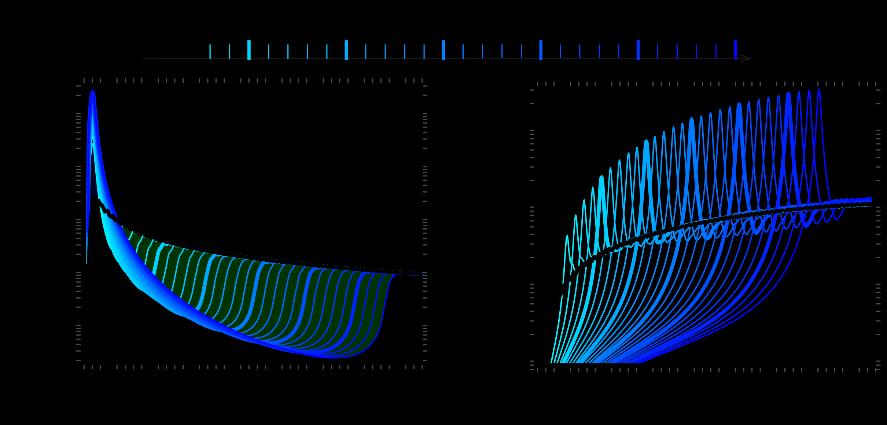
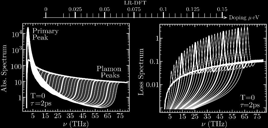
12 0T Permittivity Room T Permittivity


13 Conical Approximation & Optical Limit Kubo-Drude Formula Permittivity (LR-DFT vs KD)
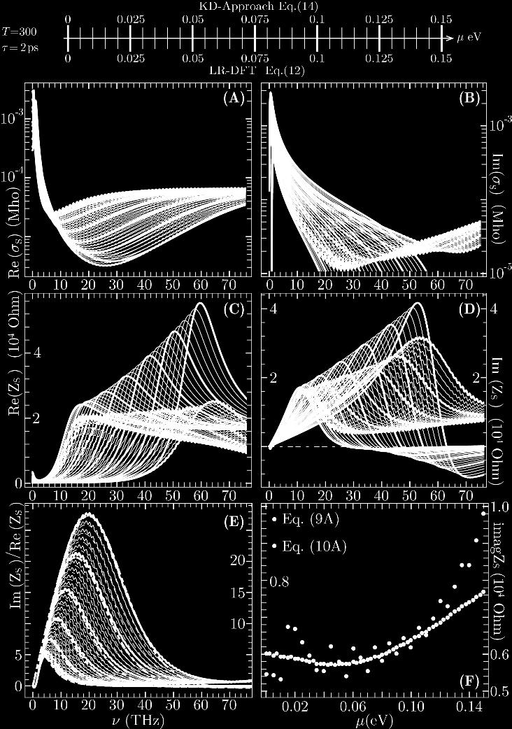
14 Conductivity-Resistivity (LR-DFT vs KD)


15 Conductivity vs Frequency Conductivity vs Time Resisitvity vs Frequency


16 Permittivity response of graphene vs an armchair nanoribbon Only LR-DFT can be used (no conical approx.)
17 We have presented advanced tools to study the linear electromagnetic response of graphene and graphene-like materials on the THz scale. Starting from an atomistic point of view, we have defined an ab initio approach in which the ground state properties of the material, i.e., energies, occupations, and one-electron wave-functions are computed by plane-wave DFT. These information are plugged in the relations of linear response theory to predict the EM response of the system, in the optical limit. Although several permittivity simulations have been performed, following similar guidelines, on pristine graphene on the ev scale, here we have defined a procedure to properly sample the electronic structure on the THz scale. At the same time, we have tested the reliability of the widely-used KD approach, operating in the same frequency range. Upon comparison of DFT-results with those obtained by the KD formulation, some significant differences have been pointed out. Nevertheless the KD formula seems to reasonably capture the main quantum features of graphene for EM applications. However, the proposed ab initio tool can be feasibly adapted to describe graphenelike systems with a more complex electronic structure than graphene, such as graphene multilayers, nano-ribbons, or nanotubes. More importantly, it has the potential to properly account for the role of metal contacts and substrate contacts. This is the object of current and future work.
18 OUTLINE Graphene and Graphene NanoRibbons: an Electromagnetic Characterization through the eyes of Linear Response Density Functional Theory THz plasmonics in graphene by Density functional theory (DFT) and Kubo derived formulation (i.e. going form theory to engineering device application)
 methods to achieve THz plasmons: spoof surface plasmons (SSP): structuring metals on a subwavelength scale (periodic corrugation, holes, etc.")
19 Motivations: THz plasmonics Science, Pendry et al., 305 (5685): o o possibility to have subwavelength confinement of the e.m. field possibility to bridge from Microwave to Optics (Conventional, i.e. non graphene like) methods to achieve THz plasmons: spoof surface plasmons (SSP): structuring metals on a subwavelength scale (periodic corrugation, holes, etc.) control dispersion by changing the geometry of the patterns use of highly doped materials, such as semiconductors and conducting polymers the conductivity can be altered by light, heat or a reversible reactions


20 THz graphene plasmonics The first plasmon observation in graphene dates back to 2012 [J. Chen et al., Nature 487, 2012] THz and mid infrared nanoimaging in graphene T. Low and P. Avouris, ACS Nano
 Some assumptions/approximations: Conical dispersion of the electron energy Plane-wave like")
21 1. Common Kubo-Drude formula for graphene Graphene je j fd fd (,,, T ) c d (1 j2 ) fd 2 fd d 2 (1 j2 ) 4 / (non-dispersive case) Some assumptions/approximations: Conical dispersion of the electron energy Plane-wave like wavefunctions
22 Linear Response Density Functional Theory (LR-DFT): a few formulas
23 1. In plane-wave DFT approaches to solid crystals, the (pseudo) band-electrons are probed the wave-functions ψ nk r = Ω 1/2 c nk+g ej k+g r G Eigenenergies ε nk Eigenbasis ψ nk 2. The corresponding band levels ε nk are populated according to the Fermi-Dirac distribution f εnk. 3. The electric displacement response to the applied electric field is given by the permittivity matrix 0 ε GG q, ω ± = ε 0 δ GG ε 0 V G q χ GG q, ω ± ε 0 V G q = q + G 2 where the independent-particle polarizability is 0 GG kq kq ( f f ) ( ) ( ) n n nn nn ( ) k k q G G q, ( ) k, nn nk n k q with the correlation terms kq ρ G nn = cnk+g c nk+q+g+g G
24 The central point is that: the DFT-based approach makes use of real electron wavefunctions Using Tight Binding wavefunctions could also be a good choice, but there are strong limits when extending the analysis to: nanoribbons, substrate effects, presence of defects, ecc.
25 DFT accuracy: experimental comparison Energy loss spectrum (directly related to the polarizability) Very good accordance up to high energies Relaxation time ~2.20 fs, and electron energy loss spectrum taken from the experiment, [T. Eberlein et al., Phys. Rev. B 77, (2008)]
 Real (Zs) Kubo")
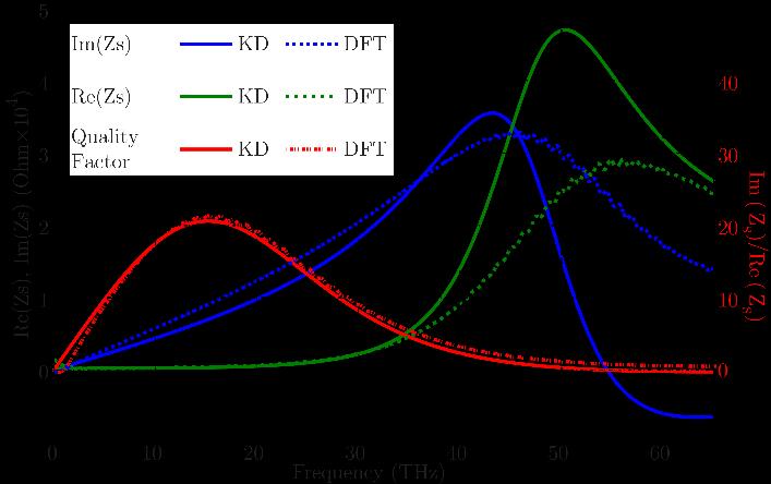
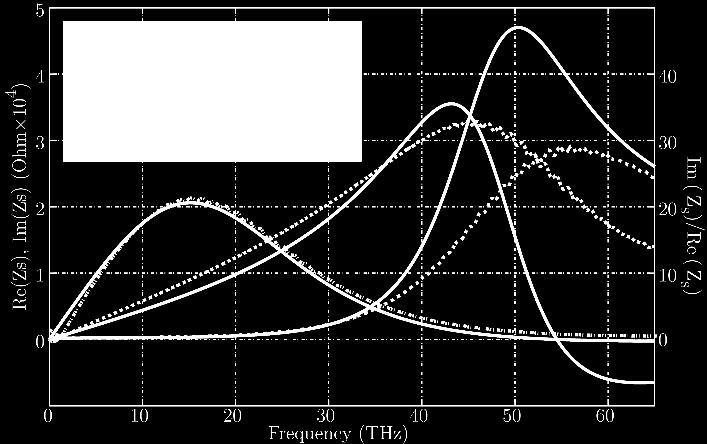
26 Comparison of the surface impedance of graphene, by DFT and Kubo-derived formula pristine and doped graphene at 300 K Imag (Zs) Real (Zs) Kubo formula DFT
/Real(Zs) Kubo formula")
27 Comparison of the plasmon quality factor, by DFT and Kubo-derived formula We define the plasmon quality factor as: Imag(Zs)/Real(Zs) Kubo formula DFT
28 Numerical example: plasmon excitation


29 Plasmon excitation by the near field of a wire antenna antenna Increasing losses (changing the mean life time) plasmon Graphene patch Some curves from the literature [2013 IEEE IELNANO, Balaban et al.]: dipole excitation of graphene disk (for different doping levels)
 strongly perturbed radiation S11 vs im(zs) high reflection")
30 Plasmon excitation Arrows: plasmon excitation Plasmon distribution vs im(zs) strongly perturbed radiation S11 vs im(zs) high reflection (detuning)
=1700 Ohm Im(Zs)=2000 Ohm E( z, r, ) G J j I 2 2 jk r r' z z' e 2 k 2 r r' z z' 2 J( z',")
31 Field radiated by the antenna (iso-surface) Low detuning High detuning through plasmon strong coupling antenna-patch Im(Zs)=1700 Ohm Im(Zs)=2000 Ohm E( z, r, ) G J j I 2 2 jk r r' z z' e 2 k 2 r r' z z' 2 J( z', r', ' ) dv '
32 Plasmon radial profile: e.m. simulation using Kubo and DFT responses Normalized electric field Fermi level ev 10 THz Kubo DFT 0 0 R/2 R Radial Position DFT plasmon with a linear increase of the charge density from the center to the edge n Normallized electric field Fermi level ev 16 THz with losses lossy neglected Increase of plasmon wavelength 0.2 R 0 0 R/2 R Radial position

 Band dispersions")
 DFT band and DOS for")
 Silicene")
33 A step forward - allowed by DFT - will be Plasmonics in 2D materials beyond graphene (in the following example: silicene) Band dispersions DOS for planar and buckled Silicene (DFT vs TB) DFT band and DOS for buckled (periodic tilt of atoms to give structural stability) Silicene and Graphene
34 Notes and conclusion 1. Up to a few THz, Kubo-Drude and DFT approaches provide similar results, but, above, differences cannot be neglected 2. Spatial dispersion (i.e. going beyond the optical limit) cannot be neglected at THz frequencies 1,2 - so the next work step: comparison between dispersive DFT and semiclassical dispersive approaches (like the Bhatnagar Gross Krook approximated model) [1] G. Lovat, G. W. Hanson t, R. Araneo and P. Burghignoli, EUCAP 2013 [2] D. C.-Serrano, J. S. G.-Diaz, and A. A.-Melcon, IEEE AWPL, Vol. 13, 2014
arxiv: v2 [cond-mat.mes-hall] 19 Sep 2015
![arxiv: v2 [cond-mat.mes-hall] 19 Sep 2015](/thumbs/89/99841565.jpg "arxiv: v2 [cond-mat.mes-hall] 19 Sep 2015") Spatial dispersion effects upon local excitation of extrinsic plasmons in a graphene micro-disk D. Mencarelli,2, S. Bellucci 2, A. Sindona 2,3, L. Pierantoni,2 Università Politecnica delle Marche, Ancona,
Spatial dispersion effects upon local excitation of extrinsic plasmons in a graphene micro-disk D. Mencarelli,2, S. Bellucci 2, A. Sindona 2,3, L. Pierantoni,2 Università Politecnica delle Marche, Ancona,
arxiv: v1 [cond-mat.mes-hall] 25 Jul 2015
![arxiv: v1 [cond-mat.mes-hall] 25 Jul 2015](/thumbs/73/69181135.jpg "arxiv: v1 [cond-mat.mes-hall] 25 Jul 2015") Spatial dispersion effects upon local excitation of extrinsic plasmons in a graphene micro-disk D. Mencarelli,2, S. Bellucci 2, A. Sindona 2,3, L. Pierantoni,2 Università Politecnica delle Marche, Ancona,
Spatial dispersion effects upon local excitation of extrinsic plasmons in a graphene micro-disk D. Mencarelli,2, S. Bellucci 2, A. Sindona 2,3, L. Pierantoni,2 Università Politecnica delle Marche, Ancona,
Optical & Transport Properties of Carbon Nanotubes II
 Optical & Transport Properties of Carbon Nanotubes II Duncan J. Mowbray Nano-Bio Spectroscopy Group European Theoretical Spectroscopy Facility (ETSF) Donostia International Physics Center (DIPC) Universidad
Optical Properties of Solid from DFT
 Optical Properties of Solid from DFT 1 Prof.P. Ravindran, Department of Physics, Central University of Tamil Nadu, India & Center for Materials Science and Nanotechnology, University of Oslo, Norway http://folk.uio.no/ravi/cmt15
Summary lecture VII. Boltzmann scattering equation reads in second-order Born-Markov approximation
 Summary lecture VII Boltzmann scattering equation reads in second-order Born-Markov approximation and describes time- and momentum-resolved electron scattering dynamics in non-equilibrium Markov approximation
Optical Properties of Semiconductors. Prof.P. Ravindran, Department of Physics, Central University of Tamil Nadu, India
 Optical Properties of Semiconductors 1 Prof.P. Ravindran, Department of Physics, Central University of Tamil Nadu, India http://folk.uio.no/ravi/semi2013 Light Matter Interaction Response to external electric
FYS Vår 2017 (Kondenserte fasers fysikk)
") FYS3410 - Vår 2017 (Kondenserte fasers fysikk) http://www.uio.no/studier/emner/matnat/fys/fys3410/v16/index.html Pensum: Introduction to Solid State Physics by Charles Kittel (Chapters 1-9, 11, 17, 18,
FYS3410 - Vår 2017 (Kondenserte fasers fysikk) http://www.uio.no/studier/emner/matnat/fys/fys3410/v16/index.html Pensum: Introduction to Solid State Physics by Charles Kittel (Chapters 1-9, 11, 17, 18,
Broadband Subwavelength Imaging with a Wire Medium Slab Loaded with Graphene Sheets
 Broadband Subwavelength Imaging with a Wire Medium Slab Loaded with Graphene Sheets Ali Forouzmand and Alexander B. Yakovlev Center for Applied Electromagnetic Systems Research (CAESR) Department of Electrical
Conductance of Graphene Nanoribbon Junctions and the Tight Binding Model
 Wu and Childs Nanoscale es Lett, 6:6 http://www.nanoscalereslett.com/content/6//6 NANO EXPE Open Access Conductance of Graphene Nanoribbon Junctions and the Tight Binding Model Y Wu, PA Childs * Abstract
An Extended Hückel Theory based Atomistic Model for Graphene Nanoelectronics
 Journal of Computational Electronics X: YYY-ZZZ,? 6 Springer Science Business Media, Inc. Manufactured in The Netherlands An Extended Hückel Theory based Atomistic Model for Graphene Nanoelectronics HASSAN
Nonlinear Electrodynamics and Optics of Graphene
 Nonlinear Electrodynamics and Optics of Graphene S. A. Mikhailov and N. A. Savostianova University of Augsburg, Institute of Physics, Universitätsstr. 1, 86159 Augsburg, Germany E-mail: sergey.mikhailov@physik.uni-augsburg.de
Electron energy loss spectroscopy (EELS)
") Electron energy loss spectroscopy (EELS) Phil Hasnip Condensed Matter Dynamics Group Department of Physics, University of York, U.K. http://www-users.york.ac.uk/~pjh503 Many slides courtesy of Jonathan
Electron energy loss spectroscopy (EELS) Phil Hasnip Condensed Matter Dynamics Group Department of Physics, University of York, U.K. http://www-users.york.ac.uk/~pjh503 Many slides courtesy of Jonathan
3-month progress Report
 3-month progress Report Graphene Devices and Circuits Supervisor Dr. P.A Childs Table of Content Abstract... 1 1. Introduction... 1 1.1 Graphene gold rush... 1 1.2 Properties of graphene... 3 1.3 Semiconductor
PBS: FROM SOLIDS TO CLUSTERS
 PBS: FROM SOLIDS TO CLUSTERS E. HOFFMANN AND P. ENTEL Theoretische Tieftemperaturphysik Gerhard-Mercator-Universität Duisburg, Lotharstraße 1 47048 Duisburg, Germany Semiconducting nanocrystallites like
Cloaking of Dielectric and Metallic Elliptical Cylinders with a Nanostructured Graphene Metasurface
 Cloaking of Dielectric and Metallic Elliptical Cylinders with a Nanostructured Graphene Metasurface Hossein M. Bernety and Alexander B. Yakovlev Center for Applied Electromagnetic Systems Research (CAESR)
Plan of the lectures
 Plan of the lectures 1. Introductory remarks on metallic nanostructures Relevant quantities and typical physical parameters Applications. Linear electron response: Mie theory and generalizations 3. Nonlinear
Project: IEEE P Working Group for Wireless Personal Area Networks (WPANs)
") Project: IEEE P802.15 Working Group for Wireless Personal Area Networks (WPANs) Title: Design of Graphene-based Nano-antennas for Terahertz Band Communication Date Submitted: 12 November, 2012 Source:
Project: IEEE P802.15 Working Group for Wireless Personal Area Networks (WPANs) Title: Design of Graphene-based Nano-antennas for Terahertz Band Communication Date Submitted: 12 November, 2012 Source:
Physical Properties of Mono-layer of
 Chapter 3 Physical Properties of Mono-layer of Silicene The fascinating physical properties[ 6] associated with graphene have motivated many researchers to search for new graphene-like two-dimensional
Graphene nanophotonics methods and devices: what can we learn from the microwave field?
 Graphene nanophotonics methods and devices: what can we learn from the microwave field? J. Perruisseau Carrier J. S. Gomez Diaz, M. Tamagnone, E. Carrasco, C. Moldovan, M. Esquius, P. Sharma, J. R. Mosig,
Plasmons in graphene: Recent progress and applications
 Plasmons in graphene: Recent progress and applications Xiaoguang Luo a, Teng Qiu a, *, Weibing Lu b, *, Zhenhua Ni a, * a Department of Physics and Key Laboratory of MEMS of the Ministry of Education,
Strained Silicon, Electronic Band Structure and Related Issues.
 Strained Silicon, Electronic Band Structure and Related Issues. D. Rideau, F. Gilibert, M. Minondo, C. Tavernier and H. Jaouen STMicroelectronics,, Device Modeling 850 rue Jean Monnet, BP 16, F-38926 Crolles
Lectures Graphene and
 Lectures 15-16 Graphene and carbon nanotubes Graphene is atomically thin crystal of carbon which is stronger than steel but flexible, is transparent for light, and conducts electricity (gapless semiconductor).
Transversal electric field effect in multilayer graphene nanoribbon
 Transversal electric field effect in multilayer graphene nanoribbon S. Bala kumar and Jing Guo a) Department of Electrical and Computer Engineering, University of Florida, Gainesville, Florida 32608, USA
Minimal Update of Solid State Physics
 Minimal Update of Solid State Physics It is expected that participants are acquainted with basics of solid state physics. Therefore here we will refresh only those aspects, which are absolutely necessary
Surface plasmon waveguides
 Surface plasmon waveguides Introduction Size Mismatch between Scaled CMOS Electronics and Planar Photonics Photonic integrated system with subwavelength scale components CMOS transistor: Medium-sized molecule
The electronic structure of materials 2 - DFT
 Quantum mechanics 2 - Lecture 9 December 19, 2012 1 Density functional theory (DFT) 2 Literature Contents 1 Density functional theory (DFT) 2 Literature Historical background The beginnings: L. de Broglie
Nanoscale optical circuits: controlling light using localized surface plasmon resonances
 Nanoscale optical circuits: controlling light using localized surface plasmon resonances T. J. Davis, D. E. Gómez and K. C. Vernon CSIRO Materials Science and Engineering Localized surface plasmon (LSP)
Lecture 11 - Phonons II - Thermal Prop. Continued
 Phonons II - hermal Properties - Continued (Kittel Ch. 5) Low High Outline Anharmonicity Crucial for hermal expansion other changes with pressure temperature Gruneisen Constant hermal Heat ransport Phonon
Quantum Condensed Matter Physics Lecture 9
 Quantum Condensed Matter Physics Lecture 9 David Ritchie QCMP Lent/Easter 2018 http://www.sp.phy.cam.ac.uk/drp2/home 9.1 Quantum Condensed Matter Physics 1. Classical and Semi-classical models for electrons
André Schleife Department of Materials Science and Engineering
 André Schleife Department of Materials Science and Engineering Yesterday you (should have) learned this: http://upload.wikimedia.org/wikipedia/commons/e/ea/ Simple_Harmonic_Motion_Orbit.gif 1. deterministic
Graphene and Carbon Nanotubes
 Graphene and Carbon Nanotubes 1 atom thick films of graphite atomic chicken wire Novoselov et al - Science 306, 666 (004) 100μm Geim s group at Manchester Novoselov et al - Nature 438, 197 (005) Kim-Stormer
PHYSICS OF SEMICONDUCTORS AND THEIR HETEROSTRUCTURES
 PHYSICS OF SEMICONDUCTORS AND THEIR HETEROSTRUCTURES Jasprit Singh University of Michigan McGraw-Hill, Inc. New York St. Louis San Francisco Auckland Bogota Caracas Lisbon London Madrid Mexico Milan Montreal
GRAPHENE NANORIBBONS TRANSPORT PROPERTIES CALCULATION. Jan VOVES
 GRAPHENE NANORIBBONS TRANSPORT PROPERTIES CALCULATION Jan VOVES Czech Technical University in Prague, Faculty of Electrical Engineering, Technicka 2, CZ-16627 Prague 6 Czech Republic, voves@fel.cvut.cz
Electrical Properties of Graphene for Interconnect Applications
 Appl. Sci. 14, 4, 35-317; doi:1.339/app435 Article OPEN ACCESS applied sciences ISSN 76-3417 www.mdpi.com/journal/applsci Electrical Properties of Graphene for Interconnect Applications Antonio Maffucci
Fig. 1: Raman spectra of graphite and graphene. N indicates the number of layers of graphene. Ref. [1]
![Fig. 1: Raman spectra of graphite and graphene. N indicates the number of layers of graphene. Ref. [1]](/thumbs/90/102653942.jpg "Fig. 1: Raman spectra of graphite and graphene. N indicates the number of layers of graphene. Ref. [1]") Vibrational Properties of Graphene and Nanotubes: The Radial Breathing and High Energy Modes Presented for the Selected Topics Seminar by Pierce Munnelly 09/06/11 Supervised by Sebastian Heeg Abstract
Vibrational Properties of Graphene and Nanotubes: The Radial Breathing and High Energy Modes Presented for the Selected Topics Seminar by Pierce Munnelly 09/06/11 Supervised by Sebastian Heeg Abstract
SCATTERING OF ELECTROMAGNETIC WAVES ON METAL NANOPARTICLES. Tomáš Váry, Juraj Chlpík, Peter Markoš
 SCATTERING OF ELECTROMAGNETIC WAVES ON METAL NANOPARTICLES Tomáš Váry, Juraj Chlpík, Peter Markoš ÚJFI, FEI STU, Bratislava E-mail: tomas.vary@stuba.sk Received xx April 2012; accepted xx May 2012. 1.
June 9, 2011, Crete, WavePro. Sergey Maksimenko, G. Ya. Slepyan Institute for Nuclear Problems, Belarus State University, Minsk, Belarus
 June 9, 2011, Crete, WavePro Carbon Nanotube as a Terahertz Delay Line: Manifestations and Potentiality in Nanoelectromagnetics Sergey Maksimenko, G. Ya. Slepyan Institute for Nuclear Problems, Belarus
Supplementary Information for Solution-Synthesized Chevron Graphene Nanoribbons Exfoliated onto H:Si(100)
") Supplementary Information for Solution-Synthesized Chevron Graphene Nanoribbons Exfoliated onto H:Si(100) Adrian Radocea,, Tao Sun,, Timothy H. Vo, Alexander Sinitskii,,# Narayana R. Aluru,, and Joseph
Supplementary Information for Solution-Synthesized Chevron Graphene Nanoribbons Exfoliated onto H:Si(100) Adrian Radocea,, Tao Sun,, Timothy H. Vo, Alexander Sinitskii,,# Narayana R. Aluru,, and Joseph
Microscopic Ohm s Law
 Microscopic Ohm s Law Outline Semiconductor Review Electron Scattering and Effective Mass Microscopic Derivation of Ohm s Law 1 TRUE / FALSE 1. Judging from the filled bands, material A is an insulator.
Is the peculiar behavior of 1/f noise. inhomogeneities?
 Is the peculiar behavior of 1/f noise in graphene the result of the interplay between band-structure and inhomogeneities? B. Pellegrini, P. Marconcini, M. Macucci, G. Fiori, and G. Basso Dipartimento di
From Graphene to Nanotubes
 From Graphene to Nanotubes Zone Folding and Quantum Confinement at the Example of the Electronic Band Structure Christian Krumnow christian.krumnow@fu-berlin.de Freie Universität Berlin June 6, Zone folding
Summary lecture VI. with the reduced mass and the dielectric background constant
 Summary lecture VI Excitonic binding energy reads with the reduced mass and the dielectric background constant Δ Statistical operator (density matrix) characterizes quantum systems in a mixed state and
sin[( t 2 Home Problem Set #1 Due : September 10 (Wed), 2008
, 2008") Home Problem Set #1 Due : September 10 (Wed), 008 1. Answer the following questions related to the wave-particle duality. (a) When an electron (mass m) is moving with the velocity of υ, what is the wave
Home Problem Set #1 Due : September 10 (Wed), 008 1. Answer the following questions related to the wave-particle duality. (a) When an electron (mass m) is moving with the velocity of υ, what is the wave
GRAPHENE NANORIBBONS Nahid Shayesteh,
 USC Department of Physics Graduate Seminar 1 GRAPHENE NANORIBBONS Nahid Shayesteh, Outlines 2 Carbon based material Discovery and innovation of graphen Graphene nanoribbons structure Application of Graphene
Outline. Introduction: graphene. Adsorption on graphene: - Chemisorption - Physisorption. Summary
 Outline Introduction: graphene Adsorption on graphene: - Chemisorption - Physisorption Summary 1 Electronic band structure: Electronic properties K Γ M v F = 10 6 ms -1 = c/300 massless Dirac particles!
Graphene for THz technology
 Graphene for THz technology J. Mangeney1, J. Maysonnave1, S. Huppert1, F. Wang1, S. Maero1, C. Berger2,3, W. de Heer2, T.B. Norris4, L.A. De Vaulchier1, S. Dhillon1, J. Tignon1 and R. Ferreira1 1 Laboratoire
Modeling of optical properties of 2D crystals: Silicene, germanene and stanene
 Modeling of optical properties of 2D crystals: Silicene, germanene and stanene Friedhelm Bechstedt 1 collaboration: L. Matthes 1 and O. Pulci 2 1 Friedrich-Schiller-Universität Jena, Germany 2 Università
Ab initio study of Mn doped BN nanosheets Tudor Luca Mitran
 Ab initio study of Mn doped BN nanosheets Tudor Luca Mitran MDEO Research Center University of Bucharest, Faculty of Physics, Bucharest-Magurele, Romania Oldenburg 20.04.2012 Table of contents 1. Density
Highly Sensitive and Wide-Band Tunable Terahertz Response of Plasma Wave based on Graphene Field Effect Transistors
 Supplementary Information Highly Sensitive and Wide-Band Tunable Terahertz Response of Plasma Wave based on Graphene Field Effect Transistors Lin Wang, Xiaoshuang Chen *, Anqi Yu, Yang Zhang, Jiayi Ding
chiral m = n Armchair m = 0 or n = 0 Zigzag m n Chiral Three major categories of nanotube structures can be identified based on the values of m and n
 zigzag armchair Three major categories of nanotube structures can be identified based on the values of m and n m = n Armchair m = 0 or n = 0 Zigzag m n Chiral Nature 391, 59, (1998) chiral J. Tersoff,
Introduction of XPS Absolute binding energies of core states Applications to silicone Outlook
 Core level binding energies in solids from first-principles Introduction of XPS Absolute binding energies of core states Applications to silicone Outlook TO and C.-C. Lee, Phys. Rev. Lett. 118, 026401
Supplemental Materials
 Supplemental Materials On the modeling of graphene layer by a thin dielectric Modeling graphene as a D surface having an appropriate value of surface conductivity σ is an accurate approach for a semiclassical
Highly Confined Tunable Mid-Infrared Plasmonics in Graphene Nanoresonators
 Supplementary Information for Highly Confined Tunable Mid-Infrared Plasmonics in Graphene Nanoresonators by Victor W. Brar, Min Seok Jang, Michelle Sherrott, Josue J. Lopez and Harry Atwater 1 Approximating
The Pennsylvania State University. The Graduate School. Electrical Engineering Department ANALYSIS AND DESIGN OF MICROWAVE AND OPTICAL
 The Pennsylvania State University The Graduate School Electrical Engineering Department ANALYSIS AND DESIGN OF MICROWAVE AND OPTICAL PLASMONIC ANTENNAS A Thesis in Electrical Engineering by Bingqian Lu
arxiv: v1 [cond-mat.mes-hall] 9 Mar 2016
![arxiv: v1 [cond-mat.mes-hall] 9 Mar 2016](/thumbs/72/68000826.jpg "arxiv: v1 [cond-mat.mes-hall] 9 Mar 2016") Dynamically controllable graphene three-port arxiv:1603.02936v1 [cond-mat.mes-hall] 9 Mar 2016 circulator Victor Dmitriev, Wagner Castro,, and Clerisson Nascimento Department of Electrical Engineering,
Dynamically controllable graphene three-port arxiv:1603.02936v1 [cond-mat.mes-hall] 9 Mar 2016 circulator Victor Dmitriev, Wagner Castro,, and Clerisson Nascimento Department of Electrical Engineering,
Summary lecture IX. The electron-light Hamilton operator reads in second quantization
 Summary lecture IX The electron-light Hamilton operator reads in second quantization Absorption coefficient α(ω) is given by the optical susceptibility Χ(ω) that is determined by microscopic polarization
Supplementary Information
 Ultrafast Dynamics of Defect-Assisted Electron-Hole Recombination in Monolayer MoS Haining Wang, Changjian Zhang, and Farhan Rana School of Electrical and Computer Engineering, Cornell University, Ithaca,
Chapter 6 Free Electron Fermi Gas
 Chapter 6 Free Electron Fermi Gas Free electron model: The valence electrons of the constituent atoms become conduction electrons and move about freely through the volume of the metal. The simplest metals
GRAPHENE the first 2D crystal lattice
 GRAPHENE the first 2D crystal lattice dimensionality of carbon diamond, graphite GRAPHENE realized in 2004 (Novoselov, Science 306, 2004) carbon nanotubes fullerenes, buckyballs what s so special about
NiS - An unusual self-doped, nearly compensated antiferromagnetic metal [Supplemental Material]
![NiS - An unusual self-doped, nearly compensated antiferromagnetic metal [Supplemental Material]](/thumbs/93/112859556.jpg "NiS - An unusual self-doped, nearly compensated antiferromagnetic metal [Supplemental Material]") NiS - An unusual self-doped, nearly compensated antiferromagnetic metal [Supplemental Material] S. K. Panda, I. dasgupta, E. Şaşıoğlu, S. Blügel, and D. D. Sarma Partial DOS, Orbital projected band structure
NiS - An unusual self-doped, nearly compensated antiferromagnetic metal [Supplemental Material] S. K. Panda, I. dasgupta, E. Şaşıoğlu, S. Blügel, and D. D. Sarma Partial DOS, Orbital projected band structure
Epsilon-Near-Zero and Plasmonic Dirac Point by using 2D materials
 Epsilon-Near-Zero and Plasmonic Dirac Point by using 2D materials Marios Mattheakis Co-authors: Prof. Efthimios Kaxiras Prof. Costas Valagiannopoulos 5-8 July 2016 NN16, Thessaloniki Graphene as Plasmonic
Introduction to Density Functional Theory with Applications to Graphene Branislav K. Nikolić
 Introduction to Density Functional Theory with Applications to Graphene Branislav K. Nikolić Department of Physics and Astronomy, University of Delaware, Newark, DE 19716, U.S.A. http://wiki.physics.udel.edu/phys824
Electronic Structure Methodology 1
 Electronic Structure Methodology 1 Chris J. Pickard Lecture Two Working with Density Functional Theory In the last lecture we learnt how to write the total energy as a functional of the density n(r): E
Metals: the Drude and Sommerfeld models p. 1 Introduction p. 1 What do we know about metals? p. 1 The Drude model p. 2 Assumptions p.
 Metals: the Drude and Sommerfeld models p. 1 Introduction p. 1 What do we know about metals? p. 1 The Drude model p. 2 Assumptions p. 2 The relaxation-time approximation p. 3 The failure of the Drude model
Radiation Diagram Control of Graphene Dipoles by Chemical Potential
 Radiation Diagram Control of Graphene Dipoles by Chemical Potential Gabriel ilva Pinto Dept. of Electrical Engineering Federal University of Para Belem, Brazil Email: gabrielp@ufpa.br Abstract This work
Road Map. Potential Applications of Antennas with Metamaterial Loading
 Road Map Potential Applications of Antennas with Metamaterial Loading Filiberto Bilotti Department of Applied Electronics University of Roma Tre Rome, Italy The history of metamaterials Metamaterial terminology
Supporting Information for Ultra-narrow metallic armchair graphene nanoribbons
 Supporting Information for Ultra-narrow metallic armchair graphene nanoribbons Supplementary Figure 1 Ribbon length statistics. Distribution of the ribbon lengths and the fraction of kinked ribbons for
Plasmonic eigenmodes in individual and bow-tie. graphene nanotriangles
 Plasmonic eigenmodes in individual and bow-tie graphene nanotriangles Weihua Wang,, Thomas Christensen,, Antti-Pekka Jauho,, Kristian S. Thygesen,, Martijn Wubs,, and N. Asger Mortensen,, DTU Fotonik,
Modern Theory of Solids
 Quantum Mechanical Approach to the Energy Bandgap Knowlton 1 Quantum Mechanical Approach to the Energy Bandgap a+ b = a o = d-spacing of 1D lattice (or plane in 3D) Knowlton 2 Symmetric vs- Asymmetric
Light Emission from Ultranarrow Graphene Nanoribbons Edge and Termini Effects. Deborah Prezzi CNR Nanoscience Institute, Modena, Italy
 Light Emission from Ultranarrow Graphene Nanoribbons Edge and Termini Effects Deborah Prezzi CNR Nanoscience Institute, Modena, Italy Graphene Nanostructures Quantum Confinement Open a band gap by confining
Supplementary Materials for
 advances.sciencemag.org/cgi/content/full/3/7/e1700704/dc1 Supplementary Materials for Giant Rashba splitting in 2D organic-inorganic halide perovskites measured by transient spectroscopies Yaxin Zhai,
Electronic and optical properties of graphene- and graphane-like SiC layers
 Electronic and optical properties of graphene- and graphane-like SiC layers Paola Gori, ISM, CNR, Rome, Italy Olivia Pulci, Margherita Marsili, Università di Tor Vergata, Rome, Italy Friedhelm Bechstedt,
Superconductivity Induced Transparency
 Superconductivity Induced Transparency Coskun Kocabas In this paper I will discuss the effect of the superconducting phase transition on the optical properties of the superconductors. Firstly I will give
Supplementary Figure 1 Magneto-transmission spectra of graphene/h-bn sample 2 and Landau level transition energies of three other samples.
 Supplementary Figure 1 Magneto-transmission spectra of graphene/h-bn sample 2 and Landau level transition energies of three other samples. (a,b) Magneto-transmission ratio spectra T(B)/T(B 0 ) of graphene/h-bn
Lecture 16: DFT for Metallic Systems
 The Nuts and Bolts of First-Principles Simulation Lecture 16: DFT for Metallic Systems Durham, 6th- 13th December 2001 CASTEP Developers Group with support from the ESF ψ k Network Overview of talk What
7.4. Why we have two different types of materials: conductors and insulators?
 Phys463.nb 55 7.3.5. Folding, Reduced Brillouin zone and extended Brillouin zone for free particles without lattices In the presence of a lattice, we can also unfold the extended Brillouin zone to get
Time-dependent density functional theory
 Time-dependent density functional theory E.K.U. Gross Max-Planck Institute for Microstructure Physics OUTLINE LECTURE I Phenomena to be described by TDDFT Some generalities on functional theories LECTURE
UNIT I: Electronic Materials.
 SIDDHARTH INSTITUTE OF ENGINEERING & TECHNOLOGY :: PUTTUR Siddharth Nagar, Narayanavanam Road 517583 QUESTION BANK (DESCRIPTIVE) Subject with Code: SEMICONDUCTOR PHYSICS (18HS0851) Course & Branch: B.Tech
Lecture 6 Photons, electrons and other quanta. EECS Winter 2006 Nanophotonics and Nano-scale Fabrication P.C.Ku
 Lecture 6 Photons, electrons and other quanta EECS 598-002 Winter 2006 Nanophotonics and Nano-scale Fabrication P.C.Ku From classical to quantum theory In the beginning of the 20 th century, experiments
Black phosphorus: A new bandgap tuning knob
 Black phosphorus: A new bandgap tuning knob Rafael Roldán and Andres Castellanos-Gomez Modern electronics rely on devices whose functionality can be adjusted by the end-user with an external knob. A new
Electronic Supplementary Material (ESI) for: Unconventional co-existence of plasmon and thermoelectric activity in In:ZnO nanowires
 for: Unconventional co-existence of plasmon and thermoelectric activity in In:ZnO nanowires") Electronic Supplementary Material (ESI) for RSC Advances. This journal is The Royal Society of Chemistry 25 Electronic Supplementary Material (ESI) for: Unconventional co-existence of plasmon and thermoelectric
Electronic Supplementary Material (ESI) for RSC Advances. This journal is The Royal Society of Chemistry 25 Electronic Supplementary Material (ESI) for: Unconventional co-existence of plasmon and thermoelectric
Electron bands in crystals Pseudopotentials, Plane Waves, Local Orbitals
 Electron bands in crystals Pseudopotentials, Plane Waves, Local Orbitals Richard M. Martin UIUC Lecture at Summer School Hands-on introduction to Electronic Structure Materials Computation Center University
Chapter 3 Properties of Nanostructures
 Chapter 3 Properties of Nanostructures In Chapter 2, the reduction of the extent of a solid in one or more dimensions was shown to lead to a dramatic alteration of the overall behavior of the solids. Generally,
Carbon nanotubes: Models, correlations and the local density of states
 Carbon nanotubes: Models, correlations and the local density of states Alexander Struck in collaboration with Sebastián A. Reyes Sebastian Eggert 15. 03. 2010 Outline Carbon structures Modelling of a carbon
Controlling Graphene Ultrafast Hot Carrier Response from Metal-like. to Semiconductor-like by Electrostatic Gating
 Controlling Graphene Ultrafast Hot Carrier Response from Metal-like to Semiconductor-like by Electrostatic Gating S.-F. Shi, 1,2* T.-T. Tang, 1 B. Zeng, 1 L. Ju, 1 Q. Zhou, 1 A. Zettl, 1,2,3 F. Wang 1,2,3
Band Structure of Isolated and Bundled Nanotubes
 Chapter 5 Band Structure of Isolated and Bundled Nanotubes The electronic structure of carbon nanotubes is characterized by a series of bands (sub- or minibands) arising from the confinement around the
Modal Interactions in Lossy Dielectric Metamaterial Slabs
 Modal Interactions in Lossy Dielectric Metamaterial Slabs A. B. Yakovlev (), G. Lovat (), P. Burghignoli (), and G. W. Hanson () () University of Mississippi () La Sapienza University of Rome () University
Optical Properties of Lattice Vibrations
 Optical Properties of Lattice Vibrations For a collection of classical charged Simple Harmonic Oscillators, the dielectric function is given by: Where N i is the number of oscillators with frequency ω
Spins and spin-orbit coupling in semiconductors, metals, and nanostructures
 B. Halperin Spin lecture 1 Spins and spin-orbit coupling in semiconductors, metals, and nanostructures Behavior of non-equilibrium spin populations. Spin relaxation and spin transport. How does one produce
2 Symmetry. 2.1 Structure of carbon nanotubes
 2 Symmetry Carbon nanotubes are hollow cylinders of graphite sheets. They can be viewed as single molecules, regarding their small size ( nm in diameter and µm length), or as quasi-one dimensional crystals
Appendix 1: List of symbols
 Appendix 1: List of symbols Symbol Description MKS Units a Acceleration m/s 2 a 0 Bohr radius m A Area m 2 A* Richardson constant m/s A C Collector area m 2 A E Emitter area m 2 b Bimolecular recombination
Monolayer Black Phosphorus
 Supporting Information: Localized Surface Plasmons in Nanostructured Monolayer Black Phosphorus Zizhuo Liu and Koray Aydin* Department of Electrical Engineering and Computer Science, Northwestern University,
(a) (b) Supplementary Figure 1. (a) (b) (a) Supplementary Figure 2. (a) (b) (c) (d) (e)
 (b) Supplementary Figure 1. (a) (b) (a) Supplementary Figure 2. (a) (b) (c) (d) (e)") (a) (b) Supplementary Figure 1. (a) An AFM image of the device after the formation of the contact electrodes and the top gate dielectric Al 2 O 3. (b) A line scan performed along the white dashed line
(a) (b) Supplementary Figure 1. (a) An AFM image of the device after the formation of the contact electrodes and the top gate dielectric Al 2 O 3. (b) A line scan performed along the white dashed line
Electron Interactions and Nanotube Fluorescence Spectroscopy C.L. Kane & E.J. Mele
 Electron Interactions and Nanotube Fluorescence Spectroscopy C.L. Kane & E.J. Mele Large radius theory of optical transitions in semiconducting nanotubes derived from low energy theory of graphene Phys.
Introduction to density functional perturbation theory for lattice dynamics
 Introduction to density functional perturbation theory for lattice dynamics SISSA and DEMOCRITOS Trieste (Italy) Outline 1 Lattice dynamic of a solid: phonons Description of a solid Equations of motion
City, University of London Institutional Repository
 City Research Online City, University of London Institutional Repository Citation: Themistos, C., Rahman, B. M., Markides, C., Uthman, M., Quadir, A. & Kejalakshmy, N. (214). Characterization of graphene-based
Nonlinear optical conductance in a graphene pn junction in the terahertz regime
 University of Wollongong Research Online Faculty of Engineering - Papers (Archive) Faculty of Engineering and Information Sciences 2010 Nonlinear optical conductance in a graphene pn junction in the terahertz
Mathematical Pattern of Plasmon Surface Selection Rules According to DrudeModel
 International Journal of Recent Research and Review, Vol. X, Issue 1, March 2017 ISSN 2277 8322 Mathematical Pattern of Plasmon Surface Selection Rules According to DrudeModel Raad A. Khamis 1,Hussam N.
The Physics of Nanoelectronics
 The Physics of Nanoelectronics Transport and Fluctuation Phenomena at Low Temperatures Tero T. Heikkilä Low Temperature Laboratory, Aalto University, Finland OXFORD UNIVERSITY PRESS Contents List of symbols
Problems. ECE 4070, Spring 2017 Physics of Semiconductors and Nanostructures Handout HW 1. Problem 1: Semiconductor History
 ECE 4070, Spring 2017 Physics of Semiconductors and Nanostructures Handout 4070 Problems Present your solutions neatly. Do not turn in rough unreadable worksheets - learn to take pride in your presentation.