Technology Excellence for Specialty Markets (and Etching Basics) Corporate Introduction
|
|
|
- Nora Magdalene Sims
- 6 years ago
- Views:
Transcription
 Corporate Introduction")
1 Technology Excellence for Specialty Markets (and Etching Basics) Corporate Introduction

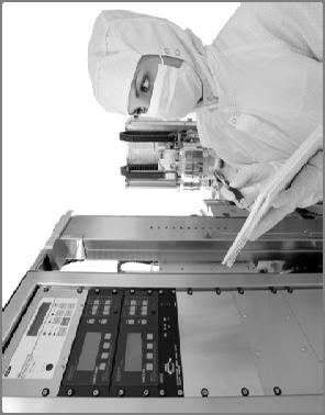
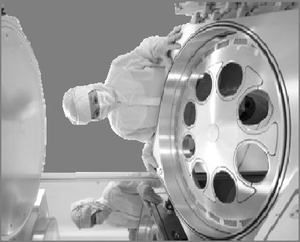
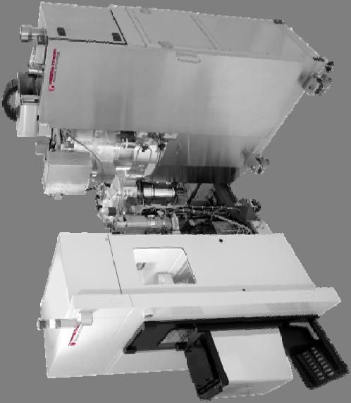
2 Semiconductor Equipment Manufacturing USA manufacturing Focus on high growth specialty markets Lab-to-Fab solutions Multiple production facilities ISO-9000/9001 Plasma-Therm, Florida, USA Advanced Vacuum Lomma, Sweden Rev-Tech, Florida, USA


3 Plasma-Therm long history of excellence Acquired by Incorporated Product Line extension Origin: RF power supplies Relocated to St. Petersburg, FL Industry first single wafer production plasma etch reactor First ever Photomask plasma etch system introduction Privately owned and operated company with headquarters in USA Industry first Plasma dicing System in production Critical machining capabilities 3


4 Etch and Deposition Solutions Leveraged Across Markets and Materials Adv. Photomask & Imprint Wireless Solid State Lighting Photonics MEMS NEMS Power Solar Data Storage Failure Analysis R&D Etch Solutions: ICP, RIE, PE, PHF-RIE, DRIE Deposition Solutions: PECVD, ICP CVD Plasma Dicing Solutions
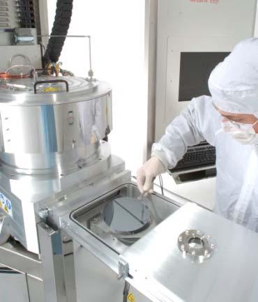
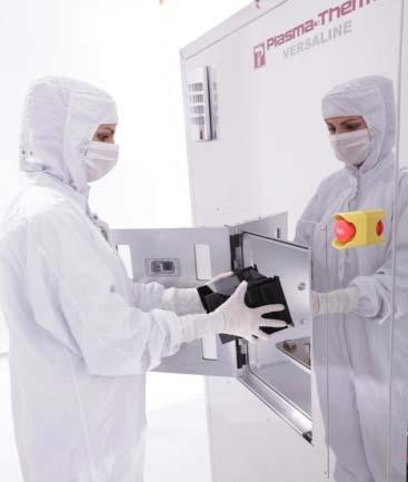
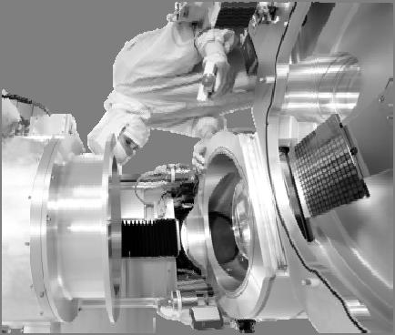
5 Configuration Flexibility From Lab to Fab Open Loadlock Cluster Fab Integration Single wafer Cassette-to-cassette

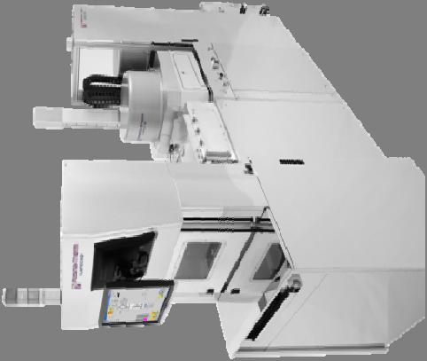


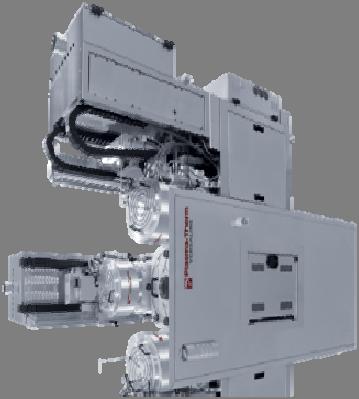

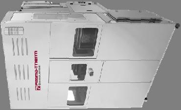

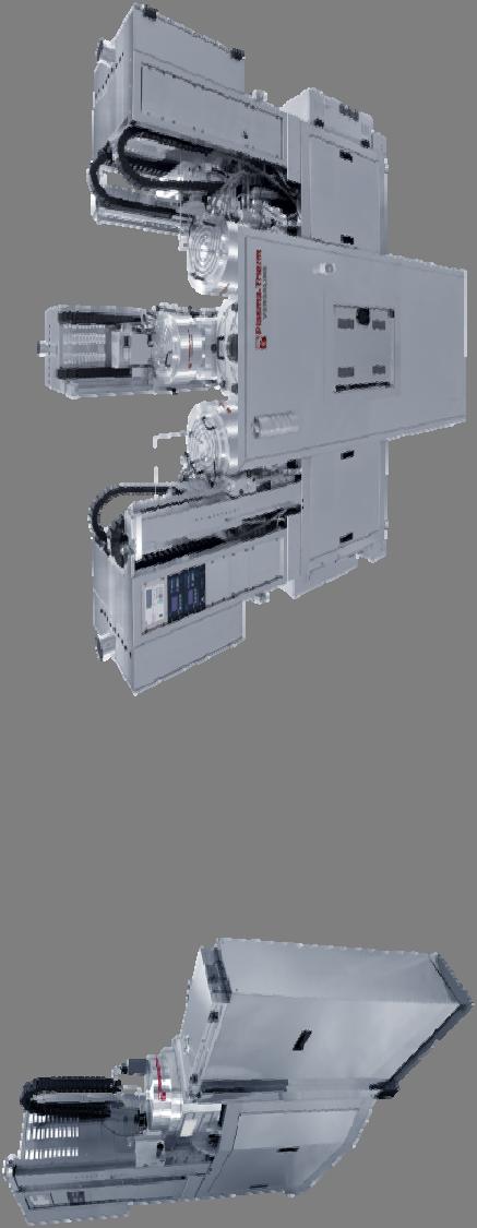
6 Product Innovation VERSALINE LAPECVD Singulator Etch and Deposition Mask Etcher


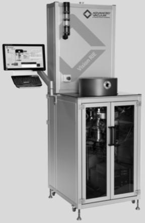
7 Advanced Vacuum product lineup Open load and single wafer loadlock Vision 300 Vision 400 Apex SLR


8 Supporting Over 640 Customers Worldwide EMEA France, Germany, Ireland, United Kingdom, Sweden, Israel, South Africa 1 Spares Warehouse Americas (St. Petersburg, FL) Sales and Service distributed throughout the US. 1 Spares warehouse location Asia-Pacific Japan, China, Taiwan, Australia, Indonesia, Korea, Singapore, India, Malaysia 4 Spares warehouses 13

9 Customer Recognized Service and Support Global service organization operating 24/7 Customer recognition of leadership VLSIresearch 10 BEST/THE BEST Awards for 17 years 2015 RANKED 1 st in Etch & Clean Equipment Suppliers 9


10 Etching Basics: Plasma Reactors Mechanisms Mask Etch Process Etching: creating faithful reproduction of a pattern 2015

 Trends and Tradeoffs Power Temperature Pressure Etching Ions Dry")
11 Plasma Etching: Fundamentals, Mechanisms, Applications Wet vs. Dry What is plasma? Hardware/reactors overview Basic Low-Pressure Processes Wet Physical Chemical etching Ion driven etching, Ion enhanced etching Ion enhanced + Inhibitor (sidewall passivation) Trends and Tradeoffs Power Temperature Pressure Etching Ions Dry Neutrals/ Radicals 11

12 Why all the Focus on Dry Etching? What s Wrong with Wet Etching? Disadvantages Limited CD geometry and control Benefits Purely chemical No physical damage Can be highly selective Wide choice of chemicals Can etch many materials Low capital cost vs. Isotropic and/or crystallographic Requires rinse and dry steps Hazardous or toxic chemicals Resist/wafer interface failure (undercutting) Potential contamination sources 3


13 Plasma Basics: Why Pursue Dry Etching? Many materials can be wet etched And plasma requires a lot of technology to make it work involves many environmental health and safety aspects is expensive But plasma can do things wet can t Less reactants required Higher purity reactants Lower contamination risk Compatible with other dry processes Anisotropic Etching (Isotropic possible) Pattern smaller geometries Improved CD control Directionality: Pattern fidelity 13
14 Plasma Basics: What is a Plasma Tornado in a Trashcan? Chemical soup, 4 th state of matter Neutrals Ions Electrons Overall charge quasi-neutral Most molecules/atoms not ionized Non-equilibrium, constant creation/loss of species Plasma electrons - small mass move fast ~9 x g Plasma ions - big mass move slow Plasma neutrals - big mass move slow Dynamic! 14

 Low")

15 Plasma Basics: How to make a plasma? Add enough energy to a gas to cause ionization Electrical Thermal Other e.g. electro-magnetic energy (radiation) Low Pressure Neon sign Very low pressure Inter-stellar space High Pressure Lightning Electric welding arc 15
16 Plasma Basics: What is an Ion? N e e - Ne + + e - Atom Electron Impact Ion + Ejected Electron 10 protons 10 electrons (2 + 8) Charge balanced Simplified view 10 protons 9 electrons (2 + 7) Extra positive charge
17 Plasma Basics: Formation of Radicals by Electron Impact (e.g. Cl 2 ) Cl 2 e - Cl + Cl Electron Impact + Cl 2 Molecule Charge balanced Happy to share an electron Full outer shell Cl Radicals Neutral but unhappy Hungry to have just one more electron to complete the outer shell Simplified view

18 Plasma Basics: What makes up plasma? Focus on RF Generated Plasma excitation frequency excitation power gas flow rate nature of gas n e = electrons concentration n o = neutral concentration n + i = positive ion concentration f(e) = distribution of energy = residence time pumping speed chamber design 7
19 Plasma Basics: Simple Plasma Processes Ion production X + e - X + + e - + e - Dissociation AB + e - A + B +e - (formation of neutrals and radicals) Ion loss mechanisms X + + e - X (unlikely) X + e - X - (electron attachment, e.g. SF 6 ) X + + wall (e - ) X (a major ion loss mechanism) Many more process than those shown Light emission X + e - X* + e - (excitation) X* X + h (photon emission) Emission at specific energy (wavelength) Used for endpoint 19
20 Basic Vacuum Processing System We ll talk about plasma a bit later Pressure Gauge Feedback Throttle Valve (controls pressure) Loadlock Plasma Process Module Turbo Mechanical Pump Pumping Speed Exhaust MFC MFC Pressure (Torr, mbar) Volume (l, cm 3, ft 3 ) Gas Flow Input MFC = mass flow controller 20


21 Basic Vacuum Processing System We ll talk about plasma in just a minute Slot valve Pressure Gauges Feedback Loadlock Plasma Process Module Turbo Mechanical Pump Exhaust Pressure Gauge MFC MFC MFC = mass flow controller Gas Flow Throttle Valve (controls pressure) 21
22 Plasma Basics: Equipment Configuration Need Low pressure Gas Electrical energy Generator - Power source Matching Network (to be discussed later) Minimizes reflected power Increases power dissipation in the discharge Protects the generator Acts as blocking capacitor RF Generator Matching Network Plasma Blocking Capacitor 22
23 Plasma Reactors: Low Density Plasma Sources Gas Inlet Matching Network RF RIE is a confusing name uses plasma (reactive species, ions) RIE technology includes other configurations RIE is a specific configuration ( plate) RIE = CCP ICP = RIE ICP Gas Inlet Powered Electrode Pump Only one RF supply No independent control of ions and radicals RF Matching Network Pump PE = Plasma Etching CCP = RIE = Reactive Ion Etching 23

24 Summary Etching is a Balance (ICP is a Good Compromise) Chemical controlled with ICP power Physical controlled with substrate bias power Neutrals - Chemical Ions - Physical Inhibitors complicate the balance 24


25 Plasma Reactors: High Density Plasma Sources B TCP MERIE ECR Magnetically Enhanced Two RF supplies More control of ions and radicals ICP 25
26 Plasma Etching Processes Many simultaneous processes Modeling gas dynamics, electromagnetics, reaction kinetics, surface interactions, etc. Excellent references to the study of plasma etching Plasma Etching: Fundamentals and Applications, M. Sugawara Handbook of Plasma Processing Technology, edited by S. Rossnagel, J. Cuomo, and W. Westwood Plasma Etching: An Introduction, D. Manos and D. Flamm misc/msc/msc1.htm D. Flamm, Pure & Appl. Chem., Vol. 62, No. 9, pp , 1990 Source: Oehrlein and Rembetski 26
27 Sputter Etching ( physical etching) High energy ions impact substrate surface and eject material - billiard ball effect Yield/Etch Rate typically decreases with increasing process pressure Etch Rate typically highest at low pressure (mtorr) Ion Sputtering 27
28 Sputter Etching Characterized by non-volatile byproducts Fluorine based chemistry (e.g. LiF, CaF: tungsten, titanium,, silicon) Chlorine based chemistry (CuCl2) No easily made byproducts (e.g. gold, platinum) High bond energies (e.g. GaN, Al 2 O 3 ), characterized by low selectivity 1/IA - Gaseous - Sputter etch 18/VIIIA H - Etchable at RT - Unknown He Li 2/IIA Be - May be able to etch 13/IIIA B 14/IVA C 15/VA N 16/VIA O 17/VIIA F Ne Na Mg VIIIB 3/IIIB 4/IVB 5/VB 6/VIB 7/VIIB /IB 12/IIB Al Si P S Cl Ar K Ca Sc Ti V Cr Mn Fe Co Ni Cu Zn Ga Ge As Se Br Kr Rb Sr Y Zr Nb Mo Tc Ru Rh Pd Ag Cd In Sn Sb Te I Xe Cs Ba * Lu Hf Ta W Re Os Ir Pt Au Hg Tl Pb Bi Po At Rn 28
29 Sputtering Process Ions create a cascade of collisions on the surface. Multiple collisions eject (or 'sputter') atoms from the surface. Sputter yield depends on : Target material (how tightly bound and density) Incoming ion mass (typically Ar, He too light, Xe too expensive, hard on turbos) Energy of the incoming ion Material Sputter Yield* Silver 3.4 Gold 2.8 Copper 2.3 Platinum 1.6 Nickel 1.5 Iron 1.3 Al 1.2 Si 0.5 Al 2 O Note: Si has very low sputter yield, so does graphite *600 ev Ar ions Source: Angstrom Sciences 29
30 Sputter Etching Purely physical Common Reactor Configuration RIE mode (common configuration) Sputtering mode with inert gas (usually Ar) Low etch rates but can remove non-volatile materials Profile may be directional (but rarely vertical) Inert Gas (e.g. Ar) Capacitive Plasma Ion energy, flux and radical conc. not independent Low selectivity- most materials sputter equally RF Matching Mask choice is important but not always a problem. Network May produce desired result Typically MHz Dirty Process products not volatile and accumulate on chamber and feature surfaces Substrate 30
31 Angular Dependence of Sputter Yield Sputter Rate θ max Max. sputter yield angle Results in enhanced etch rate at angle of max. value (θ max) Etch profile will develop at this angle faceting of mask 0 Angle (degrees) 90 θ max 31
 Not perfectly 90 at corner Resist erosion CD loss Substrate θ Example: resist after etching Angle approaches angle of max.")
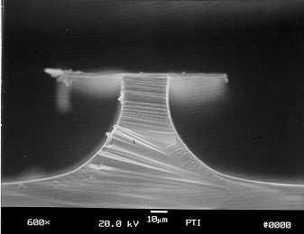
32 Sputter Etching and Development of Sloped Etch Profile As mask material is sputtered away it preferentially is lost at the corner (some part of the corner equals θ max ) Not perfectly 90 at corner Resist erosion CD loss Substrate θ Example: resist after etching Angle approaches angle of max. sputter rate 32


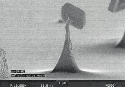
33 Sputter Etching: Mask Profile Can Affect Feature Profile Lateral erosion of resist mask can cause feature size shrinkage or roughness Photoresist Silicon Photoresist GaAs Oxide SiC Another description is that forward sputtering will always round a corner 33


34 Angled Profile Sometimes it s not a problem, it s a solution! Starting resist profile Beginning of mask faceting Mask slope transferring to feature Desired result (patterned sapphire for LED manufacturing 34

35 Sloped Masks Make Vertical Etching Difficult Selectivity = ER mask / ER film = tan(θ film )/tan(θ mask ) Use to predict slope. Selectivity Mask θ mask Best Profile


36 Sputter Etching: Can create grass or sidewall redisposition Micro-masking Often redeposited mask material Depends on mask material, bias, ion mass Tends to be less farther from masking material Not the only source of micromasking (e.g. excessive passivation, to be discussed later) 36


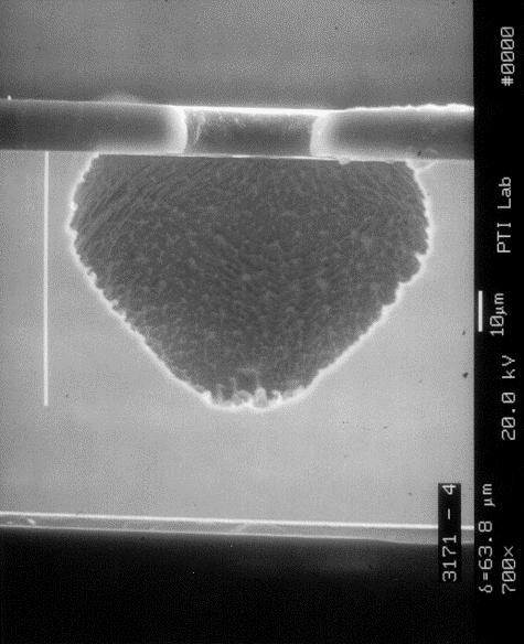
37 Sidewall redeposition Gold Etching Process Example After etch PR Re-sputter Gold Dog ears After mask removal 37


38 Sputter Etching: Can be a source of trenching Deflected ions Increased etch rate at mask edge Depends on mostly on bias and ion mass 200 W 250 W 300 W Bias Power 38
39 Chemical Etching Dominated by neutral reactive species (atoms, radicals, molecules) Radicals react with film surface Reaction is spontaneous ion assistance not required Purely isotropic (nondirectional) and low damage Reaction by-products are volatile Neutral Volatile Product Chemical Etching 39
40 Etch Product Volatility Guidance Source: C. Cardinaud et.al., Applied Surface Science 164, pp72-83 (2000) 40
41 Chemical Etching: Common Reactor Configurations RF + Match RF + Match Gas Inlet Gas Inlet Gas Inlet RF + Match Pump Pump RF + Match CCP = RIE = Reactive Ion Etching Lower electrode powered Run at low power to avoid unwanted sputtering PE = Plasma Etching Upper electrode powered Low density plasmas ICP = Inductively Coupled Plasma Etching Substrate bias and high density plasma High density plasmas 41
42 Chemical Etching Reactor Configuration PE configuration Little ion bombardment almost purely chemical etch Least flexible configuration RIE = CCP configuration High pressure operation to minimize ion reactions Low plasma/radical density (low etch rates) RF power/ion bombardment not independent ICP configuration High plasma/radical density (high etch rates) Can operate with no bias almost purely chemical etch Plasma density/ion bombardment are independent Low density plasmas High density plasmas 42
43 Chemical Etching: Examples Spontaneous etch reactions (examples) Si with SF 6 (F radical) SiN x with SF 6 (F radical) GaAs with Cl 2 (Cl radical) (Interestingly NOT etching Si with Cl 2 ) Al with Cl 2 (Cl radical) HC polymers (e.g. PR) with O 2 (O radical) Choice of chemistry can provide high selectivity SiN x /SiO 2 using SF 6 GaAs over InGaAs or AlGaAs using Cl 2 43


44 Chemical Etching: Examples Silicon trench, SF 6 GaAs, HCl (crystallographic) GaAs, Cl 2 Silicon pillar, SF 6 InP, HBr GaAs, Cl 2 44
45 Chemical Etching: Characteristics High etch rates possible High radical concentrations possible in plasma (particularly ICP) Higher density at higher pressure Rate limited by mass flow balance (what goes out, must come in) Load dependent etch rate Etch rate lower as etched area increases Consequence of mass flow balance Frequently classic bulls-eye uniformity profile Edge of substrate etches faster than center Same # radicals at substrate edge but less area 45

46 Chemical Etching: Edge Effect Edge has less area for available reactant flux Gas Phase Reactants film substrate Etch rate Edge Center Edge 46


47 Chemical Etching: Reduction of edge effect Gas Phase Reactants Physical barrier limits species access to edge film substrate Etch rate uncorrected corrected Edge Center Edge film substrate Other solutions: High pump speeds, dilution 47
48 Chemical Etching: Controlling Reaction Kinetics Modest changes in gas phase chemistry can have strong impact on etching In this case, adding ~15% O 2 increases etch rate ~4x Si + F SiF x Formation of F: CF 4 + e - CF 3 + F + e - (electron impact) CF 3 + e - CF 2 + F + e - Radical recombination: CF 3 + F CF 4 (loss of F) CF 2 + F CF 3 Addition of O 2 : (generation of F) CF 2 + O COF + F COF + O CO 2 + F Si Relative Etch Rate Addition of O 2 to CF 4 Silicon etch rate nm line intensity (F etching Si) O 2 % Source: C.J. Mogab, A.C. Adams, D.L. Flamm, J. Appl. Phys. 49, 3796 (1978) 0 Relative F Intensity 48

49 Chemistry Choice - Volatility of By-product(s) Chlorine based Fluorine based Log 10 P (mm) Refractory metals and silicides Fluorides Chlorides AlF AlCl sub Cu 2 F Cu 3 Cl TiF TiCl WF 6 18 WCl Source: T.P. Chow, A.J. Steckl, Electron Devices, IEEE Transactions, 11, 1983 Use vapor pressures when available or boiling points as a guide when they are not 49
50 Chemistry Choice - Volatility of By-product(s) Chemistry Primary Films Etched Cl based ( e.g. Cl 2, BCl 3, SiCl 4 ) Al (+ alloys), Ti, TiN, W, Cr, Hf, W, Mo F based (e.g. SF 6, CF 4, CHF 3 ) Ti, W, TiW, WN, Mo, Ta, silicides Other factors play a role: masking materials additive gases, film quality, desired results, etc. 50
51 Ion Enhanced Etching Physical and chemical components: individually slow but together increase the etch rate and anisotropy Combination of radicals and ions etch wafer Ions striking the surface enhance reactions and product desorption Ion Product Neutral Ion Enhanced 51
52 Ion Enhanced Etching: Common Reactor Configurations RF + Match Gas Inlet Gas Inlet RF + Match Pump CCP = RIE configuration Low pressure operation to maximize ion formation Low plasma/radical density (low etch rates) Ion density/ion energy not independent RF + Match ICP configuration High ion density Plasma density/ion bombardment are independent ICP power ion and radical densities Bias power Ion energy 52
 Tachi (1985) Damage & enhancement Coburn & Winters (1978) > 10x etch rate increase spontaneous sputtered Source: J.W. Coburn, H.")
53 Ion Enhanced Etching Experiment shows role of ions/radicals Illustrates the dramatic affect of combining radicals and ions Radicals Radicals + Ions Only Ions XeF 2 Ar+ Ar+ ion XeF gas ion + 2 beam gas only beam only Ion enhanced Models Reactive spot (energy addition) Tachi (1985) Damage & enhancement Coburn & Winters (1978) > 10x etch rate increase spontaneous sputtered Source: J.W. Coburn, H.F. Winters, J. Appl. Phys. 50, 3189 (1979) 53
54 Other early studies of ion effects Source: Pabst et al., Int. J. Mass Spect. Ion Phys. 20, 191 (1976) Source: J.W. Coburn, H.F. Winters, J. Appl. Phys. 50, 3189 (1979) Si etching with Ar+ CF 4 CF 4 is not adsorbed on Si surface Al with Ar+ + F 2 Low volatility of AlF 3, Al alone sputters faster Si etching with Ar+ Cl 2 SiCl 4 volatile Source: J.W. Coburn, H.F. Winters, J. Appl. Phys. 50, 3189 (1979) 54
55 Ion Enhanced Etching Ions contribute to anisotropy Example: XeF 2 etching of Si Anisotropy 1 Higher anisotropy with higher energy ions Penalty for anisiotropy by increasing ion flux or energy but typically lower selectivity, trenching, damage XeF 2 Flow rate Source: P. Martin, Vacuum Technology & Coating,, 28, (Nov. 2009) (Not the original reference) 55


56 Ion Enhanced Etching Examples SiC with SF 6 : ions assist formation of SiF x and CF x etch products Al 2 O 3 with BCl 3 : ions assist formation of AlCl x etch products SiO 2 with CF 4 : ions assist formation of Si and C etch products GaN with Cl 2 : ions assist desorption of GaCl x etch products 56
57 Ion Enhanced Etching Ion bombardment is necessary to break strong bonds Si O 8.2 ev Al O 9.3 ev By products must still be volatile (e.g. SiF 4, AlCl 3 ) Vertical ion bombardment vertical etch Mask erosion may result in sloped profile (similar to sputter etch) Choice of radicals can provide selectivity e.g. etching SiO 2 with CF 4 (CF 2 and CF 3 radicals) Selectivity less than Chemical etch and greater than Sputter etch Loading effects < chemical etch Rate rarely mass flow limited 57
 Inhibitor")
")


58 Ion Enhanced Etching + Inhibitor (Sidewall passivation) Inhibitor Reactant Ion Product Inhibitor Inhibitor (often polymer forming) can passivate surfaces Minimal ion bombardment on sidewalls to remove inhibitor Surface protected from etching Passivation removed from horizontal surfaces by ion bombardment Surface open for etching (chemical or ion assisted) 58

59 Ion Enhanced Etching + Inhibitor Most highly anisotropic processes fall in this category Inhibitor introduced intentionally Si etch using SF 6 plus C 4 F 8 Al etch using BCl 3 /Cl 2 plus CH 4 InP etch using HBr or Cl 2 plus N 2 undercut Inhibitor introduced unintentionally Etching using photo resist mask Resist etch by-product is polymer precursor Etch result depends on resist loading Anisotropic etch with resist mask, isotropic with hard mask e.g. GaAs via etch with resist mask Source: after M. Mieth and A. Barker, Semiconductor International, 5, 222 (May, 1984) 59
60 Materials which act as inhibitors Photoresist etch by-product (particularly from Cl etch) Hydrocarbons e.g. CH 4 Chlorinated hydrocarbons e.g. CHCl 3 (most banned) Freons CHF 3 ~= C 4 F 8 > C 2 F 6 > CF 4 F:C ratio and oxidation capability of surface determines effectiveness as polymer precursor (e.g. O from SiO2 can provide oxidation source) N 2 for some processes, e.g. Al, InP O 2 can oxidize sidewall e.g. silicon (e.g. cryo black silicon process) 60


61 Ion Enhanced Etching + Inhibitor Example: Multilayer InP/InGaAs/InP Isotropic etch induced notch in feature profile HBr/CH 4 /BCl 3 Preferentially etches InGaAs layer HBr/N 2 Inhibition of InGaAs etching Requires understanding of how inhibitors participate (e.g. CH 4 sometimes an inhibitor, sometimes an etchant 61
 using Ar/Cl 2 Resist by-products provide sidewall passivation")
62 Ion Enhanced Etching + Inhibitor Polymer provides sidewall protection Anisotropic GaAs etch (via etch) using Ar/Cl 2 Resist by-products provide sidewall passivation 62


 40 um vias Cl 2 partial")
63 GaAs Profile Control - Isotropic to Anisotropic Selectivity increases with Cl 2 partial pressure: etch rate and isotropy increases Resist implicated in controlling profile GaAs Etch Rate (um/min) Etch Selectivity (GaAs:PR) 40 um vias Cl 2 partial pressure (mtorr) 63


64 Tungsten Etch Example SF 6 / CF 4 / Ar F for reaction, CF 4 for passivation Vertical profile Sidewall roughness transferred from mask roughness PR Al W Before etch Al W Process temperature 20 C Selectivity to PR ~5:1 ~2000 A/min After etch 64
65 Tungsten Etching with Fluorine Chemistry Relative F Atom Density (arb. Units) CF 4 / O 2 Etch rate (nm/min) Relative F Atom Density (arb. Units) SF 6 / O 2 Etch rate (nm/min) CF 4 / O 2 vs. SF 6 / O 2 : Etch rate and Relative F Atom Density F is primary etchant (similar activation energies) for SF 6 and CF 4 O 2 increase rate for CF 4 /O 2 with more available F. O and F compete for W sites O 2 decrease rate for SF 6 /O 2, interaction with SF x and W? (adding O2 doesn t help) Source: Tang and Hess, J. Electrochem. Soc. 131, 115 (1984) Mark Salimian, Plasma Etching, Technologies and Processes,
66 Mask material is often important PR SiO 2 W RIE with SF 6 PR SiN x W SiO 2 W SiN x W Data suggests O from SiO 2 attacks sulfur (S) protection layer on W More efficient removal of inhibitor than N from SiNx Source: Sato et al, 7 th Plasma Process Symp. Proceedings Electrochem. Soc. 1988, p240 Source: Mark Salimian, Plasma Etching, Technologies and Processes,
67 Ion Enhanced Etching + Inhibitor Characteristics Often involved in achieving anisotropic profiles Balance of etchant and inhibitor Profile, uniformity sensitive to ratio Too little inhibitor, profile isotropic Too much inhibitor, etch rate decreases, polymer formation, micro-masking Excess inhibitor deposition causing grass Balance can change with Aspect ratio (mass transfer issues) Temperature sensitive Polymer deposition (affects profile) changes with temperature Potential for deposition on chamber surfaces Reduced at elevated temperatures 67
68 Al Etch General Considerations Typical Al process steps: Breakthrough (remove native oxide) Main etch Post etch treatment Material composition issues Al-Si: Si residues may require post F-plasma treatment (e.g. CF 4 ) to remove unetched Si (this may impact underlayer) Al-Cu: Cu difficult to etch, susceptible to grassing from precipitates Requires higher temperature and more ion bombardment Cu 3 Cl 3 a temperature of about 200 C Al deposition quality: no O 2 present Reduce Al 2 O 3 formation during deposition: no leaks, loadlock, high purity Ar Al 2 O 3 formation from poor vacuum conditions (e.g. leaks, outgassing) Mask profile (sloped, rough, or poor adhesion) Corrosion (post etch) 68
69 Al Etching Another example of sidewall passivation Photoresist erosion assists sidewall passivation Resist condition (e.g. slope, bake temperature) Surface AlCl 3 reacts with moisture exposure to make HCl which corrodes Al Cl residues in resist & sidewall deposits also react to form HCl Treatments In-situ PR strip (O 2 ash) (best) F replacement of Cl using CF 4 (O 2 ) (possibly SF 6 ) CHF 3 will deposit polymer protecting the wafer from moisture attack. Immediate rinsing of wafer and removal of resist after Al etch High temperature bake (usually not available due to PR) C O Photoresist Al Substrate Sidewall film Al Cl 69
70 Al Etching Breakthrough Removal of Native oxide Surface reacts to ambient atmosphere to make 20-50Å Al 2 O 3 Cl 2 alone won t work. Al 2 O 3 + Cl 2 AlCl 3 + O 2 (makes more Al 2 O 3 ) BCl 3 to needed to reduce Al 2 O 3 Al 2 O 3 + BCl 3 AlCl 3 + B 2 O 3 (BOCl) BCl 3 acts as an O 2 scavenger CCl x could be used but carcinogenic (Al 2 O 3 + CCl x (x 4) AlCl 3 + CO) Even with reducing chemistry and energetic ion bombardment, the etch rate of Al 2 O 3 is >300x less than Al Cl Cl Cl Cl Cl Cl Cl Cl Cl Surface oxide A 2 O 3 Al 2 O 3 Surface reoxidized Al Al + O 2 Cl 2 Al Al 70
71 Al Etching Main Etch Al (unlike Al 2 O 3 ) can be etched in Cl 2 (or with Br Cl 2 reacts spontaneously at RT (without plasma or ion bombardment) Cl Cl Cl Cl Cl Cl Cl Al 2 AlCl 3 or (AlCl 3 ) 2 Al Al AlCl 3 sufficiently volatile at 20 C to desorb Desire high pumping speed (low residence ) reduces AlCl 3 partial pressure Heated chamber walls (reduce re-deposition) Load lock (safety and low oxygen presence) Highly load dependent (chemical component) may require diffusion barriers to improve uniformity) Al not etched in F-containing gases. AlF 3 only volatile at elevated temperatures (i.e. chamber should be free of F) Al Al 71


72 Plasma Etch Feature Profile Defects Physical effects (ions) Mask faceting Ion scattering Off-angle ions Neutral beam solutions? Bowing Mask Facet Trenching Ion Reflection Undercut Under Passivation Chemical effects Over passivation Under passivation Taper Over passivation Notching Charging Re-entrance Ion Scatter Tilt-Skew Ion Trajectory Source: adapted from Donnelly, V. M. and Kornbilt, A., J. Vac. Sci. Technol. A 31, (2013)
 Recombination centers Surface morphology Insulator breakdown/leakage Depth can be surprisingly deep Surface to many 100s Å Many sources 73")
73 Damage Effects Process and device dependent Multiple types of damage can result from processes Ion damage to lattice (e.g. ion penetration, vacancies, interstitials) Carrier passivation (carrier concentrations) Surface contamination (surface states) (e.g. fluorocarbon layers) Recombination centers Surface morphology Insulator breakdown/leakage Depth can be surprisingly deep Surface to many 100s Å Many sources 73


74 Damage examples Source: Seiji Samukawa et al 2012 J. Phys. D: Appl. Phys Buried Quantum Well Photoluminescence for Monitoring Etch Damage Depth H ion penetrates ~5x deeper Source: Wong, Green, Liu, Lishan, Bellis, Hu, Petroff, Holtz, Merz, J. Vac. Sci. Technol. B 6 (6) 1906 (1988) UV/VUV penetrates deeper with O2 plasma but fewer defects near surface
75 Damage Example InP Etching: RIE vs. ICP CH 4 /H 2 chemistry RIE has lower etch rate RIE 2x P surface loss enhanced Source: Cardinaud, C, et al,., Appl. Surface Science, 164 (2000) RIE P depleted layer ~2x ICP RIE 2-3x thicker amorphous layer 75
76 Summary - Etching Mechanisms Ion Neutral Ion Product Sputtering Ion Enhanced Neutral Volatile Product Inhibitor Neutral Ion Product Inhibitor Chemical Ion Enhanced + Inhibitor 76
77 Summary Basic Low Pressure Etching Mechanisms Sputter Etching Ions strike surface and eject or sputter material Nonvolatile reaction products Chemical Etching Neutral dominated (atoms, radicals, molecules) Isotropic, non-directional, can be reagent limited Ion Driven Etching Ions strike surface and enhance reactions Both physical and chemical components Allows fast anisotropic etching Ion Enhanced + Inhibitor Formation Polymer forming components passivate sidewalls where ion bombardment is minimal Prevention of lateral etching 77
78 Pressure Effects Strong effects Ion Energy Physical (sputtering) Low pressure Stronger ion influence More directional (CD control) Potential for more damage Ion flux Neutral flux Ion Assisted (chemical and physical High pressure Requires additional control mechanism (e.g. passivation) More neutral influence Neutral flux Ion flux Chemical (radicals) Ratio of sheath thickness Pressure (mtorr) and mean free path of ion
79 Pressure Effects Strong effects Affects ion energy, density, bias, electron temperature Reduction in pressure increases electron temperature and this results in increase in DC bias (more electrons leave the plasma) Chemical based processes etch rate usually increases with pressure (longer residence time for reactants) Ion enhanced processes Etch rate might actually decrease with increasing pressure (lower ion energies) Profile affected: mass transport (lag), sidewall passivation 79

80 Power Effects Increased ICP power increased concentration of radicals Increased electrode bias power increased DC bias Increases the effect of ions (more energetic and more of them) Mask erosion increases selectivity decreases Possible to actually have better selectivity if material of interest etch rate goes up faster than mask erosion Wafer cooling becomes more important as either ICP or bias power increases Wafer gets hot with all the energy being delivered (and exothermic reactions) Need to manage thermal budget! 80
81 Temperature Effects Wafer temperature affects etch rate, selectivity, surface roughness and anisotropy Chemical processes affected the most Temperature, isotropy (and often roughness) Temperature, Etch rate Temperature, Selectivity (usually but not always) Consider Si etching masked by SiO 2 (example) Rate F(SiO2) = 6.14 x n F T 1/2 e /kT Å/min Rate F(Si) = 2.91 x n F T 1/2 e /kT Å/min Selectivity = R F(Si) /R F(SiO2) = 4.7 e /kT ( higher T, lower selectivity) Changes in T can have large effect on selectivity (e.g. InP etching) Photoresist etch rate increases with temperature Source: Flamm et al., VLSI Electronics, Vol. 8, Chap (1984) 81
82 General Process Trends Process Parameter Etch Rate Response with Increase in Process Parameter Selectivity (to mask) Mechanism Trend Uniformity Bias Power Increases Decreases More physical Weak effect Electrode Size (power density) Decreases Increases Less physical Weak effect Source Power Increases Increases More chemical Weak effect Pressure Substrate Temperature Usually increases Weak effect More chemical Usually worse Increases Depends More chemical Weak effect Important Caveat: material dependent 82
83 Advanced Plasma Developments Interest in removing ions & controlling neutral energies Multiple frequencies Pulsed gases Pulsing ICP source Pulsing bias Neutral control grids, ion filters ALE Atomic Layer Etching Temporal Spatial RF Bias Source: adapted from Ankur Agarwal et. al., J. of Applied Physics, 106, , (2009) 83
84 Temporal Etching Atomic Layer Etching (ALE) Flush Adsorb Volatize Flush 84
85 Time-Multiplexed Etching Atomic Layer Etching (ALE) Potential Benefits Monolayer control of etch Elimination of profile defects Elimination of ARDE Limitations Extremely low etch rates Narrow process window to achieve monolayer control Status Demonstrated in Si Cl-based chemistries 4 step cycle demonstrated 280 ALE cycles 150sec cycle times Source: Donnelly, V. M. and Kornbilt, A., J. Vac. Sci. Technol. A 31, (2013). 85

, 73-82 (2013).")
86 Spatially Multiplexed Etching DRIE Spatial DRIE Approach Spatial ALD Reactor Source: Roozeboom, F. et al., ECS Trans. 50 (32), (2013). 86
87 Summary Usually there are Tradeoffs Uniformity Profile Etching Rate Damage Selectivity Surface Morphology 87
88 Thank you
ETCHING Chapter 10. Mask. Photoresist
 ETCHING Chapter 10 Mask Light Deposited Substrate Photoresist Etch mask deposition Photoresist application Exposure Development Etching Resist removal Etching of thin films and sometimes the silicon substrate
Reactive Ion Etching (RIE)
") Reactive Ion Etching (RIE) RF 13.56 ~ MHz plasma Parallel-Plate Reactor wafers Sputtering Plasma generates (1) Ions (2) Activated neutrals Enhance chemical reaction 1 2 Remote Plasma Reactors Plasma Sources
Reactive Ion Etching (RIE) RF 13.56 ~ MHz plasma Parallel-Plate Reactor wafers Sputtering Plasma generates (1) Ions (2) Activated neutrals Enhance chemical reaction 1 2 Remote Plasma Reactors Plasma Sources
Etching Issues - Anisotropy. Dry Etching. Dry Etching Overview. Etching Issues - Selectivity
 Etching Issues - Anisotropy Dry Etching Dr. Bruce K. Gale Fundamentals of Micromachining BIOEN 6421 EL EN 5221 and 6221 ME EN 5960 and 6960 Isotropic etchants etch at the same rate in every direction mask
Plasma etching. Bibliography
 Plasma etching Bibliography 1. B. Chapman, Glow discharge processes, (Wiley, New York, 1980). - Classical plasma processing of etching and sputtering 2. D. M. Manos and D. L. Flamm, Plasma etching; An
Section 3: Etching. Jaeger Chapter 2 Reader
 Section 3: Etching Jaeger Chapter 2 Reader Etch rate Etch Process - Figures of Merit Etch rate uniformity Selectivity Anisotropy d m Bias and anisotropy etching mask h f substrate d f d m substrate d f
ORBITAL DIAGRAM - A graphical representation of the quantum number "map" of electrons around an atom.
 160 ORBITAL DIAGRAM - A graphical representation of the quantum number "map" of electrons around an atom. 4p 3d 4s 3p 3s 2p 2s 1s Each blank represents an ORBITAL, and can hold two electrons. The 4s subshell
Device Fabrication: Etch
 Device Fabrication: Etch 1 Objectives Upon finishing this course, you should able to: Familiar with etch terminology Compare wet and dry etch processes processing and list the main dry etch etchants Become
Etching: Basic Terminology
 Lecture 7 Etching Etching: Basic Terminology Introduction : Etching of thin films and sometimes the silicon substrate are very common process steps. Usually selectivity, and directionality are the first
ORBITAL DIAGRAM - A graphical representation of the quantum number "map" of electrons around an atom.
 178 (MAGNETIC) SPIN QUANTUM NUMBER: "spin down" or "spin up" - An ORBITAL (region with fixed "n", "l" and "ml" values) can hold TWO electrons. ORBITAL DIAGRAM - A graphical representation of the quantum
E SC 412 Nanotechnology: Materials, Infrastructure, and Safety Wook Jun Nam
 E SC 412 Nanotechnology: Materials, Infrastructure, and Safety Wook Jun Nam Lecture 10 Outline 1. Wet Etching/Vapor Phase Etching 2. Dry Etching DC/RF Plasma Plasma Reactors Materials/Gases Etching Parameters
CHEMICAL COMPOUNDS MOLECULAR COMPOUNDS
 48 CHEMICAL COMPOUNDS - Dalton's theory does not mention this, but there is more than one way for atoms to come together to make chemical compounds! - There are TWO common kinds of chemical compound, classified
CHEMICAL COMPOUNDS MOLECULAR COMPOUNDS
 48 CHEMICAL COMPOUNDS - Dalton's theory does not mention this, but there is more than one way for atoms to come together to make chemical compounds! - There are TWO common kinds of chemical compound, classified
How many grams of sodium metal is required to completely react with 2545 grams of chlorine gas?
 EXAMPLE PROBLEM: How many grams of sodium metal is required to completely react with 2545 grams of chlorine gas? 1 - Convert 2545 grams of chlorine to moles chlorine using formula weight 2 - Convert moles
EE 527 MICROFABRICATION. Lecture 25 Tai-Chang Chen University of Washington
 EE 527 MICROFABRICATION Lecture 25 Tai-Chang Chen University of Washington ION MILLING SYSTEM Kaufmann source Use e-beam to strike plasma A magnetic field applied to increase ion density Drawback Low etch
-"l" also contributes ENERGY. Higher values for "l" mean the electron has higher energy.
 170 - Giving the four parameters will uniquely identify an electron around an atom. No two electrons in the same atom can share all four. These parameters are called QUANTUM NUMBERS. PRINCIPAL QUANTUM
CHAPTER 6: Etching. Chapter 6 1
 Chapter 6 1 CHAPTER 6: Etching Different etching processes are selected depending upon the particular material to be removed. As shown in Figure 6.1, wet chemical processes result in isotropic etching
-"l" also contributes ENERGY. Higher values for "l" mean the electron has higher energy.
 175 - Giving the four parameters will uniquely identify an electron around an atom. No two electrons in the same atom can share all four. These parameters are called QUANTUM NUMBERS. PRINCIPAL QUANTUM
Experiment Three. Lab two: Parts 2B and 3. Halogens used in Parts 2 and 3. Lab one: Parts 1 and 2A. Halogens (Family VIIA) used in Parts 2 and 3
 used in Parts 2 and 3") Experiment Three Lab one: Parts 1 and 2A Lab two: Parts 2B and 3 1 1A 1 H 1s 1 2 IIA 3 Li 2s 1 1 1 Na 3s 1 1 9 K 4s 1 3 7 Rb 5s 1 5 5 Cs 6s 1 8 7 Fr 7s 1 4 Be 2s 2 1 2 Mg 3s 2 3 IIIB 4 IVB 5 VB 6 VIB 7
Experiment Three Lab one: Parts 1 and 2A Lab two: Parts 2B and 3 1 1A 1 H 1s 1 2 IIA 3 Li 2s 1 1 1 Na 3s 1 1 9 K 4s 1 3 7 Rb 5s 1 5 5 Cs 6s 1 8 7 Fr 7s 1 4 Be 2s 2 1 2 Mg 3s 2 3 IIIB 4 IVB 5 VB 6 VIB 7
CHEMICAL COMPOUNDS MOLECULAR COMPOUNDS
 48 CHEMICAL COMPOUNDS - Dalton's theory does not mention this, but there is more than one way for atoms to come together to make chemical compounds! - There are TWO common kinds of chemical compound, classified
Lewis dot structures for molecules
 1 Lewis dot structures for molecules In the dot structure of a molecule, - SHARED valence electrons are shown with dashes - one per pair. - UNSHARED valence electrons ("lone pairs") are represented by
... but using electron configurations to describe how aluminum bromide forms is a bit cumbersome! Can we simplify the picture a bit?
 193... but using electron configurations to describe how aluminum bromide forms is a bit cumbersome! Can we simplify the picture a bit? LEWIS NOTATION / ELECTRON-DOT NOTATION - Lewis notation represents
VIIIA He IIA IIIA IVA VA VIA VIIA. Li Be B C N O F Ne. Na Mg VIB VIIB VIIIB IB IIB S. K Ca Sc Ti V Cr Mn Fe Co Ni Cu Zn Ga Ge As Se Br
 188 THE FIRST TWO PERIODIC TRENDS IN A NUTSHELL LARGER IONIZATION ENERGY SMALLER RADIUS IA H IIA IIIA IVA VA VIA VIIA VIIIA He Li Be B C N O F Ne Na Mg IIIB IVB VB Al Si P VIB VIIB VIIIB IB IIB S Cl Ar
Example: Helium has an atomic number of 2. Every helium atom has two protons in its nucleus.
 59 Atomic terms - ATOMIC NUMBER: The number of protons in the atomic nucleus. Each ELEMENT has the SAME NUMBER OF PROTONS in every nucleus. In neutral atoms, the number of ELECTRONS is also equal to the
Placeholder zeros, even though they aren't SIGNIFICANT, still need to be included, so we know how big the number is!
 28 A few more math with significant figures examples: 15047 11 0.9876 Placeholder zeros, even though they aren't SIGNIFICANT, still need to be included, so we know how big the number is! Addition: 147.3
8. Relax and do well.
 CHEM 1314 3;30 pm Theory Exam III John III. Gelder November 13, 2002 Name TA's Name Lab Section INSTRUCTIONS: 1. This examination consists of a total of 8 different pages. The last page include a periodic
How many grams of sodium metal is required to completely react with 2545 grams of chlorine gas?
 146 EXAMPLE PROBLEM: How many grams of sodium metal is required to completely react with 2545 grams of chlorine gas? 1 - Convert 2545 grams of chlorine gas to moles. Use formula weight. 2 - Convert moles
CHEM 10113, Quiz 5 October 26, 2011
 CHEM 10113, Quiz 5 October 26, 2011 Name (please print) All equations must be balanced and show phases for full credit. Significant figures count, show charges as appropriate, and please box your answers!
Fall 2011 CHEM Test 4, Form A
 Fall 2011 CHEM 1110.40413 Test 4, Form A Part I. Multiple Choice: Clearly circle the best answer. (60 pts) Name: 1. The common constituent in all acid solutions is A) H 2 SO 4 B) H 2 C) H + D) OH 2. Which
Putting it together... - In the early 20th century, there was a debate on the structure of the atom. Thin gold foil
 36 Putting it together... - In the early 20th century, there was a debate on the structure of the atom. RUTHERFORD EXPERIMENT Where do the particles go? Radioactive material A few bounce back A few particles
The Stanford Nanofabrication Facility. Etch Area Overview. May 21, 2013
 The Stanford Nanofabrication Facility Etch Area Overview May 21, 2013 High Density Plasma Systems Etcher Materials Etched Gases available Wafer Size Applied Materials P5000 MRIE ChA Applied Materials P5000
Atomic weight: This is a decimal number, but for radioactive elements it is replaced with a number in parenthesis.
 47 Blocks on the periodic table 11 Sodium 22.99 Atomic number: This is always a whole number. The periodic table is arranged by atomic number! Element symbol: A one or two letter abbreviation for the name
- Light has properties of WAVES such as DIFFRACTION (it bends around small obstructions).
.") 170 LIGHT wavelength Diffraction frequency = wavelengths / time = - Light has properties of WAVES such as DIFFRACTION (it bends around small obstructions). - Einstein noted that viewing light as a particle
170 LIGHT wavelength Diffraction frequency = wavelengths / time = - Light has properties of WAVES such as DIFFRACTION (it bends around small obstructions). - Einstein noted that viewing light as a particle
CVD: General considerations.
 CVD: General considerations. PVD: Move material from bulk to thin film form. Limited primarily to metals or simple materials. Limited by thermal stability/vapor pressure considerations. Typically requires
WRITING AN IONIC FORMULA
 WRITING AN IONIC FORMULA - if you know the ions that make up a compound, all you need to do is find the smallest ratio of cation to anion the compound needs to have an overall charge of zero Example: If
Halogens HALOGENS. Parts 2A and 2B. Chem : Feb. 19, 20 and March 3. Compare the properties and reactivity of the halogens and halides
 Chem. 125-126: Feb. 19, 20 and March 3 Experiment 3 Session 2 (Three hour lab) Complete Experiment 3 Parts 2B and 3 Complete team report Complete discussion presentation Parts 2A and 2B Compare the properties
CHEMICAL COMPOUNDS. - Dalton's theory does not mention this, but there is more than one way for atoms to come together to make chemical compounds!
 69 CHEMICAL COMPOUNDS - Dalton's theory does not mention this, but there is more than one way for atoms to come together to make chemical compounds! - There are TWO common kinds of chemical compound, classified
Periodic Table. Modern periodic table
 41 Periodic Table - Mendeleev (1869): --- When atoms are arranged in order of their atomic weight, some of their chemical and physical properties repeat at regular intervals (periods) --- Some of the physical
- Atomic line spectra are UNIQUE to each element. They're like atomic "fingerprints".
 - Atomic line spectra are UNIQUE to each element. They're like atomic "fingerprints". - Problem was that the current model of the atom completely failed to explain why atoms emitted these lines. An orbit
(FIRST) IONIZATION ENERGY
 IONIZATION ENERGY") 181 (FIRST) IONIZATION ENERGY - The amount of energy required to remove a single electron from the outer shell of an atom. - Relates to reactivity for metals. The easier it is to remove an electron, the
181 (FIRST) IONIZATION ENERGY - The amount of energy required to remove a single electron from the outer shell of an atom. - Relates to reactivity for metals. The easier it is to remove an electron, the
- Some properties of elements can be related to their positions on the periodic table.
 179 PERIODIC TRENDS - Some properties of elements can be related to their positions on the periodic table. ATOMIC RADIUS - The distance between the nucleus of the atoms and the outermost shell of the electron
The Periodic Table of the Elements
 The Periodic Table of the Elements All matter is composed of elements. All of the elements are composed of atoms. An atom is the smallest part of an element which still retains the properties of that element.
Atomic weight: This is a decimal number, but for radioactive elements it is replaced with a number in parenthesis.
 47 Blocks on the periodic table 11 Sodium 22.99 Atomic number: This is always a whole number. The periodic table is arranged by atomic number! Element symbol: A one or two letter abbreviation for the name
Periodic Table. - Mendeleev was able to predict the properties of previously unknown elements using his "periodic law" Modern periodic table
 74 Periodic Table - Mendeleev (1869): --- When atoms are arranged in order of their atomic weight, some of their chemical and physical properties repeat at regular intervals (periods) --- Some of the physical
EE 527 MICROFABRICATION. Lecture 24 Tai-Chang Chen University of Washington
 EE 527 MICROFABRICATION Lecture 24 Tai-Chang Chen University of Washington EDP ETCHING OF SILICON - 1 Ethylene Diamine Pyrocatechol Anisotropy: (100):(111) ~ 35:1 EDP is very corrosive, very carcinogenic,
Periodic Table. Modern periodic table
 41 Periodic Table - Mendeleev (1869): --- When atoms are arranged in order of their atomic weight, some of their chemical and physical properties repeat at regular intervals (periods) --- Some of the physical
Atomic terms. Example: Helium has an atomic number of 2. Every helium atom has two protons in its nucleus.
 Atomic terms - ATOMIC NUMBER: The number of protons in the atomic nucleus. Each ELEMENT has the SAME NUMBER OF PROTONS in every nucleus. In neutral atoms, the number of ELECTRONS is also equal to the atomic
VIIIA H PREDICTING CHARGE
 58 IA PREDICTING CHARGE VIIIA H IIA IIIA IVA VA VIA VIIA You can reliably determine the charge using our method for Groups IA, IIA, IIIB, Aluminum, and the Group VA, VIA, and VIIA NONMETALS Li Be B C N
NUCLEAR MODEL. Electron cloud. Electron cloud. Nucleus. Nucleus
 37 NUCLEAR MODEL - Atoms are mostly empty space - NUCLEUS, at the center of the atom, contains protons and neutrons. This accounts for almost all the mass of an atom - Electrons are located in a diffuse
- A CHEMICAL BOND is a strong attractive force between the atoms in a compound. attractive forces between oppositely charged ions
 191 CHEMICAL BONDS - A CHEMICAL BOND is a strong attractive force between the atoms in a compound. 3 TYPES OF CHEMICAL BOND Ionic bonds attractive forces between oppositely charged ions sodium chloride
Example: If a simple ionic compound is made of these two ions, what is its formula? In the final formula, don't write the charges on the ions!
 88 WRITING AN IONIC FORMULA - if you know the ions that make up a compound, all you need to do is find the smallest ratio of cation to anion the compound needs to have an overall charge of zero Example:
CHEMICAL COMPOUNDS MOLECULAR COMPOUNDS
 48 CHEMICAL COMPOUNDS - Dalton's theory does not mention this, but there is more than one way for atoms to come together to make chemical compounds! - There are TWO common kinds of chemical compound, classified
Solutions and Ions. Pure Substances
 Class #4 Solutions and Ions CHEM 107 L.S. Brown Texas A&M University Pure Substances Pure substance: described completely by a single chemical formula Fixed composition 1 Mixtures Combination of 2 or more
- Some properties of elements can be related to their positions on the periodic table.
 186 PERIODIC TRENDS - Some properties of elements can be related to their positions on the periodic table. ATOMIC RADIUS - The distance between the nucleus of the atoms and the outermost shell of the electron
- Some properties of elements can be related to their positions on the periodic table.
 180 PERIODIC TRENDS - Some properties of elements can be related to their positions on the periodic table. ATOMIC RADIUS - The distance between the nucleus of the atoms and the outermost shell of the electron
Lecture 15 Etching. Chapters 15 & 16 Wolf and Tauber. ECE611 / CHE611 Electronic Materials Processing Fall John Labram 1/76
 Lecture 15 Etching Chapters 15 & 16 Wolf and Tauber 1/76 Announcements Term Paper: You are expected to produce a 4-5 page term paper on a selected topic (from a list). Term paper contributes 25% of course
Atomic structure. The subatomic particles. - a small, but relatively massive particle that carres an overall unit POSITIVE CHARGE
 35 Atomic structure - Until the early 20th century, chemists considered atoms to be indivisible particles. - The discovery of SUBATOMIC PARTICLES changed the way we view atoms! PROTON NEUTRON ELECTRON
WRITING AN IONIC FORMULA
 55 WRITING AN IONIC FORMULA - if you know the ions that make up a compound, all you need to do is find the smallest ratio of cation to anion the compound needs to have an overall charge of zero Example:
- Dalton's theory sets LIMITS on what can be done with chemistry. For example:
 34 - Dalton's theory sets LIMITS on what can be done with chemistry. For example: Chemistry can't convert lead (an element) into gold (another element). Sorry, alchemists! You can't have a compound form
(please print) (1) (18) H IIA IIIA IVA VA VIA VIIA He (2) (13) (14) (15) (16) (17)
 (1) (18) H IIA IIIA IVA VA VIA VIIA He (2) (13) (14) (15) (16) (17)") CHEM 10113, Quiz 3 September 28, 2011 Name (please print) All equations must be balanced and show phases for full credit. Significant figures count, show charges as appropriate, and please box your answers!
CHEM 10113, Quiz 3 September 28, 2011 Name (please print) All equations must be balanced and show phases for full credit. Significant figures count, show charges as appropriate, and please box your answers!
- Why are phase labels required? Because phase changes either absorb or release energy. ... what does this mean?
 157 SINCE the enthalpy change does NOT depend on path, this means that we can use standard values for enthalpy to predict the heat change in reactions that we have not tested in a calorimeter. THERMOCHEMICAL
- A CHEMICAL BOND is a strong attractive force between the atoms in a compound. attractive forces between oppositely charged ions
 CHEMICAL BONDS - A CHEMICAL BOND is a strong attractive force between the atoms in a compound. 3 TYPES OF CHEMICAL BOND Ionic bonds attractive forces between oppositely charged ions sodium chloride Covalent
1.02 Elements, Symbols and Periodic Table
 .0 Elements, Symbols and Periodic Table Dr. Fred O. Garces Chemistry Miramar College.0 Elements, Symbols and the Periodic Table January 0 The Elements: Building block of Matter The periodic table of the
INSTRUCTIONS: Exam III. November 10, 1999 Lab Section
 CHEM 1215 Exam III John III. Gelder November 10, 1999 Name TA's Name Lab Section INSTRUCTIONS: 1. This examination consists of a total of 7 different pages. The last page includes a periodic table and
Lecture 11. Etching Techniques Reading: Chapter 11. ECE Dr. Alan Doolittle
 Lecture 11 Etching Techniques Reading: Chapter 11 Etching Techniques Characterized by: 1.) Etch rate (A/minute) 2.) Selectivity: S=etch rate material 1 / etch rate material 2 is said to have a selectivity
IONIC COMPOUNDS. - USUALLY form from metals combining with nonmetals, or from metals combining with metalloids
 52 IONIC COMPOUNDS - USUALLY form from metals combining with nonmetals, or from metals combining with metalloids Examples: - almost always solid at room temperature, and usually have relatively high melting
Plasma Deposition (Overview) Lecture 1
 Lecture 1") Plasma Deposition (Overview) Lecture 1 Material Processes Plasma Processing Plasma-assisted Deposition Implantation Surface Modification Development of Plasma-based processing Microelectronics needs (fabrication
Plasma Deposition (Overview) Lecture 1 Material Processes Plasma Processing Plasma-assisted Deposition Implantation Surface Modification Development of Plasma-based processing Microelectronics needs (fabrication
WRITING AN IONIC FORMULA
 55 WRITING AN IONIC FORMULA - if you know the ions that make up a compound, all you need to do is find the smallest ratio of cation to anion the compound needs to have an overall charge of zero Example:
Course theme. Three hours of lab Complete E1 (Parts 1, 2, 3, 4, and 5B) Prepare discussion presentation Prepare team report.
 Prepare discussion presentation Prepare team report.") Experiment Session 2 Electrons and Solution Color Three hours of lab Complete E (Parts, 2, 3, 4, and 5B) Prepare discussion presentation Prepare team report. Course theme There are structure and property
Experiment Session 2 Electrons and Solution Color Three hours of lab Complete E (Parts, 2, 3, 4, and 5B) Prepare discussion presentation Prepare team report. Course theme There are structure and property
Three hours of lab Complete E1 (Parts 1, 2, 3, 4, and 5B) Prepare discussion presentation Prepare team report. Course theme
 Prepare discussion presentation Prepare team report. Course theme") Experiment 1 Session 2 Electrons and Solution Color Three hours of lab Complete E1 (Parts 1, 2, 3, 4, and 5B) Prepare discussion presentation Prepare team report. Course theme There are structure and property
Experiment 1 Session 2 Electrons and Solution Color Three hours of lab Complete E1 (Parts 1, 2, 3, 4, and 5B) Prepare discussion presentation Prepare team report. Course theme There are structure and property
E5 Lewis Acids and Bases: lab 2. Session two lab Parts 2B, 3, and 4. Session one lab Parts 1and 2A. Aquo Complex Ions. Aquo Complex Ion Reactions
 E5 Lewis Acids and Bases: lab 2 Session one lab Parts 1and 2A Part 2B. Complexation, Structure and Periodicity Compare the reactivity of aquo complex ions containing pre-transition, transition, and post-transition
VIIIA H PREDICTING CHARGE
 58 IA PREDICTING CHARGE VIIIA H IIA IIIA IVA VA VIA VIIA You can reliably determine the charge using our method for Groups IA, IIA, IIIB, Aluminum, and the Group VA, VIA, and VIIA NONMETALS Li Be B C N
Chapter 7 Plasma Basic
 Chapter 7 Plasma Basic Hong Xiao, Ph. D. hxiao89@hotmail.com www2.austin.cc.tx.us/hongxiao/book.htm Hong Xiao, Ph. D. www2.austin.cc.tx.us/hongxiao/book.htm 1 Objectives List at least three IC processes
8. Relax and do well.
 CHEM 1515 Exam II John II. Gelder October 14, 1993 Name TA's Name Lab Section INSTRUCTIONS: 1. This examination consists of a total of 8 different pages. The last two pages include a periodic table, a
EXAMPLES. He VIA VIIA Li Be B C N O F Ne
 59 IA EXAMPLES VIIIA H IIA IIIA IVA VA He VIA VIIA Li Be B C N O F Ne Na Mg IIIB IVB VB Al Si P VIB VIIB VIIIB IB IIB S Cl Ar K Ca Sc Ti V Cr Mn Fe Co Ni Cu Zn Ga Ge As Se Br Kr Rb Sr Y Zr Nb Mo Tc Ru
4.06 Periodic Table and Periodic Trends
 4.06 Periodic Table and Periodic Trends Dr. Fred Omega Garces Chemistry 100, Miramar College 1 4.06 Periodic Table and Periodic Trend The Periodic Table and the Elements What is the periodic table? What
E5 Lewis Acids and Bases: lab 2. Session two lab Parts 2B, 3, and 4. Session one lab Parts 1and 2A. Aquo Complex Ions
 E5 Lewis Acids and Bases: lab 2 Session one lab Parts 1and 2A Session two lab Parts 2B, 3, and 4 Part 2B. Complexation, Structure and Periodicity Compare the reactivity of aquo complex ions containing
8. Relax and do well.
 CHEM 1014 Exam I John I. Gelder September 16, 1999 Name TA's Name Lab Section Please sign your name below to give permission to post your course scores on homework, laboratories and exams. If you do not
Acids. Lewis Acids and Bases. Lewis Acids. Lewis acids: H + Cu 2+ Al 3+ E5 Lewis Acids and Bases (Session 1) March 19-24
 March 19-24") E5 Lewis Acids and Bases (Session 1) March 19-24 Session one Pre-lab (p.151) due 1st hour discussion of E4 Lab (Parts 1and 2A) Session two Lab: Parts 2B, 3 and 4 Acids Bronsted: Acids are proton donors.
E5 Lewis Acids and Bases (Session 1) March 19-24 Session one Pre-lab (p.151) due 1st hour discussion of E4 Lab (Parts 1and 2A) Session two Lab: Parts 2B, 3 and 4 Acids Bronsted: Acids are proton donors.
Wet and Dry Etching. Theory
 Wet and Dry Etching Theory 1. Introduction Etching techniques are commonly used in the fabrication processes of semiconductor devices to remove selected layers for the purposes of pattern transfer, wafer
E5 Lewis Acids and Bases. Acids. Acids. Session one. Session two Lab: Parts 2B, 3 and 4
 E5 Lewis Acids and Bases Session one Pre-lab (p.141) due at start of lab. First hour: Discussion of E4 Lab: Parts 1and 2A Session two Lab: Parts 2B, 3 and 4 Acids Bronsted: Acids are proton donors and
- Some properties of elements can be related to their positions on the periodic table.
 179 PERIODIC TRENDS - Some properties of elements can be related to their positions on the periodic table. ATOMIC RADIUS - The distance between the nucleus of the atoms and the outermost shell of the electron
8. Relax and do well.
 CHEM 34.02 and 34.03 Name Exam III John III. Gelder TA's Name November 5, 2000 Lab Section INSTRUCTIONS:. This examination consists of a total of 9 different pages. The last three pages include a periodic
UNIT 3. By: Ajay Kumar Gautam Asst. Prof. Dev Bhoomi Institute of Technology & Engineering, Dehradun
 UNIT 3 By: Ajay Kumar Gautam Asst. Prof. Dev Bhoomi Institute of Technology & Engineering, Dehradun 1 Syllabus Lithography: photolithography and pattern transfer, Optical and non optical lithography, electron,
4FNJDPOEVDUPS 'BCSJDBUJPO &UDI
 2010.5.4 1 Major Fabrication Steps in CMOS Process Flow UV light oxygen Silicon dioxide Silicon substrate Oxidation (Field oxide) photoresist Photoresist Coating Mask exposed photoresist Mask-Wafer Exposed
Circle the letters only. NO ANSWERS in the Columns! (3 points each)
") Chemistry 1304.001 Name (please print) Exam 4 (100 points) April 12, 2017 On my honor, I have neither given nor received unauthorized aid on this exam. Signed Date Circle the letters only. NO ANSWERS in
Chemistry 1304.001 Name (please print) Exam 4 (100 points) April 12, 2017 On my honor, I have neither given nor received unauthorized aid on this exam. Signed Date Circle the letters only. NO ANSWERS in
Atomic Emission Spectra. and. Flame Tests. Burlingame High School Chemistry
 Atomic Structure Atomic Emission Spectra and Flame Tests Flame Tests Sodium potassium lithium When electrons are excited they bump up to a higher energy level. As they bounce back down they release energy
Lecture 6 Plasmas. Chapters 10 &16 Wolf and Tauber. ECE611 / CHE611 Electronic Materials Processing Fall John Labram 1/68
 Lecture 6 Plasmas Chapters 10 &16 Wolf and Tauber 1/68 Announcements Homework: Homework will be returned to you on Thursday (12 th October). Solutions will be also posted online on Thursday (12 th October)
Regents of the University of California
 Deep Reactive-Ion Etching (DRIE) DRIE Issues: Etch Rate Variance The Bosch process: Inductively-coupled plasma Etch Rate: 1.5-4 μm/min Two main cycles in the etch: Etch cycle (5-15 s): SF 6 (SF x+ ) etches
INSTRUCTIONS: CHEM Exam I. September 13, 1994 Lab Section
 CHEM 1314.05 Exam I John I. Gelder September 13, 1994 Name TA's Name Lab Section Please sign your name below to give permission to post, by the last 4 digits of your student I.D. number, your course scores
Bronsted: Acids are proton donors. Session one Pre-lab (p.151) due 1st hour discussion of E4 Lab (Parts 1and 2A)
 due 1st hour discussion of E4 Lab (Parts 1and 2A)") E5 Lewis Acids and Bases (Session 1) November 5-11 Acids Bronsted: Acids are proton donors. Session one Pre-lab (p.151) due 1st hour discussion of E4 Lab (Parts 1and 2A) Problem Compounds containing cations
E5 Lewis Acids and Bases (Session 1) November 5-11 Acids Bronsted: Acids are proton donors. Session one Pre-lab (p.151) due 1st hour discussion of E4 Lab (Parts 1and 2A) Problem Compounds containing cations
4.01 Elements, Symbols and Periodic Table
 .0 Elements, Symbols and Periodic Table Dr. Fred O. Garces Chemistry 00 Miramar College.0 Elements, symbols and the Periodic Table Aug The Elements: Building block of Matter The periodic table of the chemical
8. Relax and do well.
 CHEM 1215 Exam III John III. Gelder November 11, 1998 Name TA's Name Lab Section INSTRUCTIONS: 1. This examination consists of a total of 7 different pages. The last page includes a periodic table and
Chapter 12 The Atom & Periodic Table- part 2
 Chapter 12 The Atom & Periodic Table- part 2 Electrons found outside the nucleus; negatively charged Protons found in the nucleus; positive charge equal in magnitude to the electron s negative charge Neutrons
7. Relax and do well.
 CHEM 1215 Exam II John II. Gelder October 7, 1998 Name TA's Name Lab Section INSTRUCTIONS: 1. This examination consists of a total of 5 different pages. The last page includes a periodic table and a solubility
Plasma Chemistry Study in an Inductively Coupled Dielectric Etcher
 Plasma Chemistry Study in an Inductively Coupled Dielectric Etcher Chunshi Cui, John Trow, Ken Collins, Betty Tang, Luke Zhang, Steve Shannon, and Yan Ye Applied Materials, Inc. October 26, 2000 10/28/2008
LECTURE 5 SUMMARY OF KEY IDEAS
 LECTURE 5 SUMMARY OF KEY IDEAS Etching is a processing step following lithography: it transfers a circuit image from the photoresist to materials form which devices are made or to hard masking or sacrificial
Three hour lab. Chem : Feb Experiment 2 Session 2. Experiment 2 Session 2 Electrons and Solution Color
 Chem.25-26: Feb. 5 - Experiment 2 Session 2 Preparation Pre-lab prep and reading for E2, Parts 3-5 Experiment 2 Session 2 Electrons and Solution Color Three hour lab Complete E2 (Parts - 5) Prepare discussion
HANDOUT SET GENERAL CHEMISTRY II
 HANDOUT SET GENERAL CHEMISTRY II Periodic Table of the Elements 1 2 3 4 5 6 7 1 2 3 4 5 6 7 8 9 10 11 12 13 14 15 16 17 18 IA VIIIA 1 2 H He 1.00794 IIA IIIA IVA VA VIA VIIA 4.00262 3 Li 6.941 11 Na 22.9898
8. Relax and do well.
 CHEM 1314 Name Exam IV TA Name John IV. Gelder December 14, 1992 Lab Section INSTRUCTIONS: 1. This examination consists of a total of 9 different pages. The last three pages includes a periodic table and
CHEM 130 Exp. 8: Molecular Models
 CHEM 130 Exp. 8: Molecular Models In this lab, we will learn and practice predicting molecular structures from molecular formulas. The Periodic Table of the Elements IA 1 H IIA IIIA IVA VA VIA VIIA 3 5