CHEMICAL VAPOR DEPOSITION (CVD)
|
|
|
- Roland McBride
- 6 years ago
- Views:
Transcription
1
2 CHEMICAL VAPOR DEPOSITION (CVD) A process of formation of a non-volatile solid film on a substrate from the reaction of vapor phase chemical reactants containing the right proportion of constituents. ELEMETRY STEPS IN CVD : Introduction of reactive species into a reactor Diffusion and Adsorption of the reactants onto the surface Reaction at the surface to form the solid Desorption of by products from the surface Diffusion of by products and un-reacted reactants away from the surface and transport of by products out of the reactor
3 Deposition rate is determined by rate limiting step Effluents out of the reactor Effluents out of the reactor Substrate ZnS (s) + H2 (g), H Zn Adsorption & reaction H2S Ar Zn fu f i D Diffusion of by-products Zn Ar e h t of n sio ts n a ct a e r H2 S H2 S fu f i D Ar Zn + Ar ts n a act H y-products Diffusion of b H H2S (g) + Zn (g) re e Ar th of n sio H2 S Ar H2 S H2S Ar Ar Zn H2S + Ar Reactive species into a reactor
4 CONTROL OF ELEMENTARY STEPS Chemical Reactions Reactor Type and Geometry Process parameters (Temperature, Pressure, Flow rate and time) Transport phenomena (Mass and Heat) Kinetics and Thermodynamics Hence, CVD technique combines several scientific and engineering disciplines
5 CVD Reactor Types CVD Type Advantageous Disadvantages APCVD 100 mbar mbar Simple, Fast, Low temperature Contamination Non uniformity LPCVD 1 mbar 30 mbar Purity, Uniformity Slower, Vacuum, High Temperature PECVD 1 mbar 10 mbar 100kHz to 2.45 GHz Fast, Low temp. Contamination Cost Laser Induced CVD Metal-organic CVD Plasma Assisted CVD High Density CVD L-CVD MOCVD PACVD HDCVD Vapor Phase Epitaxy Atomic Layer Deposition VPE ALCVDD Cold wall CVD : Only substrate heating by Inductive heating( RF, eddy), Optical heating (lamp), Resistive heating ( suceptor) Adv/Disadv. No deposition in chamber walls but temp. monitoring and uniformity are issues. Hot Wall CVD : Heat entire system and generally used.
6 TYPICAL CVD REACTIONS Example : CH4 + TiCl4 TIC + 4HCl BCl3 + NH3 BN + 3HCl SIH4 + NH3 Si3N4 +H2 CH3Cl3Si +H2 SiC + 3HCl Mastering the process chemical reaction by the mastering the technology


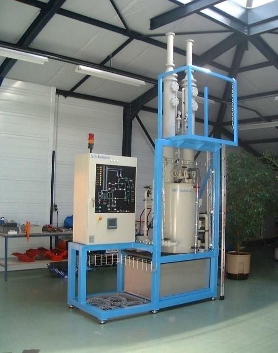
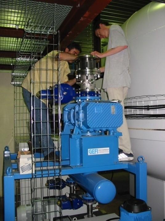
7 MPA Industrie expertizes : Design and construction of customized turn key CVD reactors. Chemical and physical engineering of reactor Special gas handling ( toxic, corosive, explosible) Liquid source handling (storage and dosing) specialist Solid source development : high temperature chlorination of metal Vacuum technic and effluent trapping Process control


8 SPECIAL GAS AND LIQUID SOURCE HANDLING


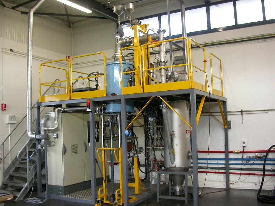
9 Reactor design whatever the size Temperature up to 2200 C RF, DC, MW plasmas
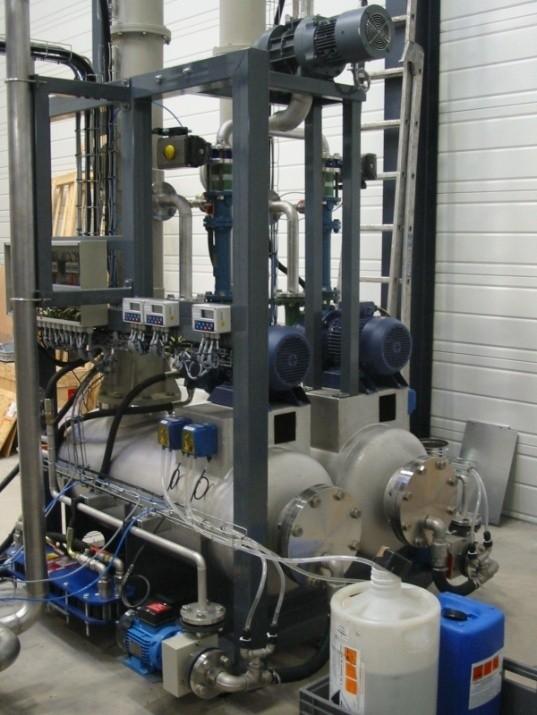
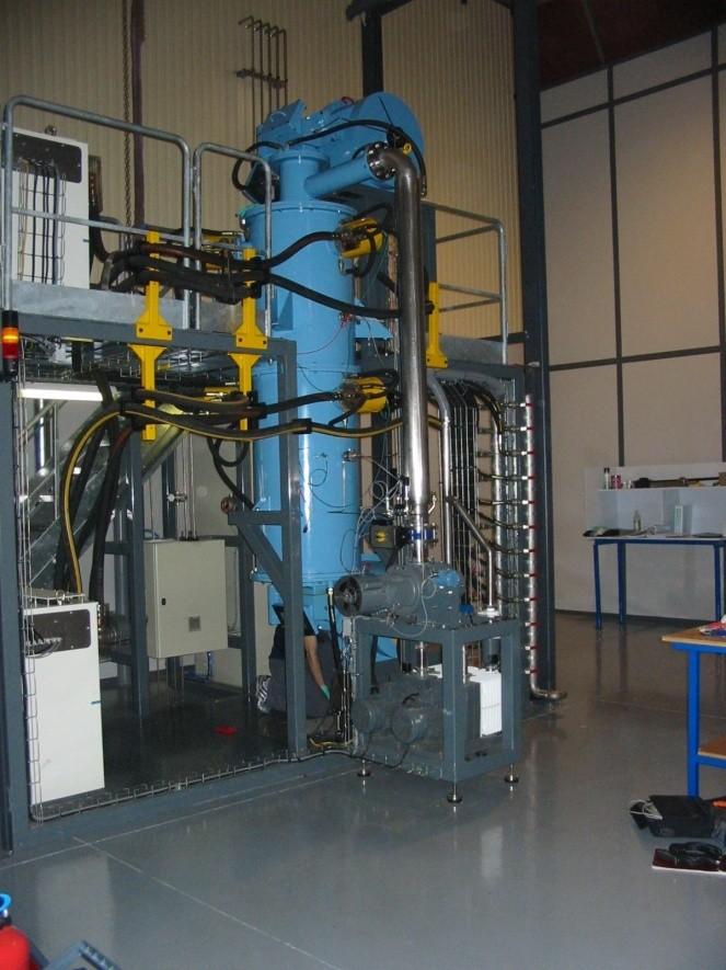
10 Vacuum techniques applied to CVD processes Dry and wet scrubbing stations

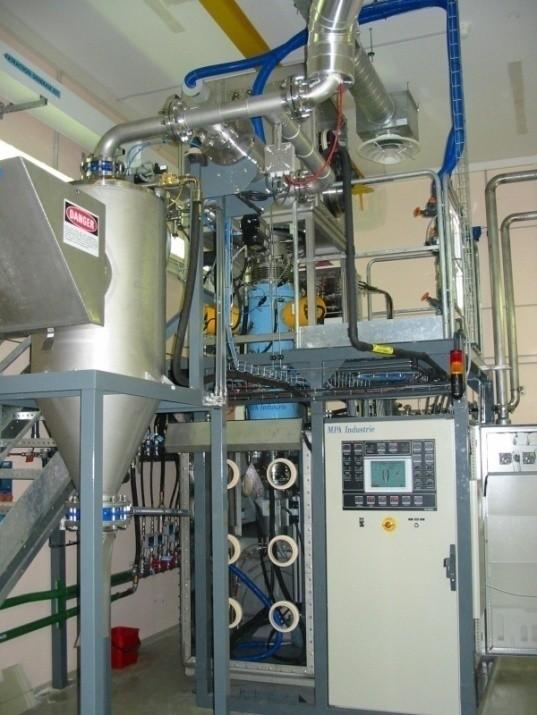
11 PROCESS CONTROL


12 FULL OFFER Hazardous analysis Chemical field knowledge Nuclear field knowledge CVD consultancy CAD departement


13 LARGE FIELD OF ACTION FROM LABORATORY SCALE TO INDUSTRIAL SCALE

14 Process mastering: Thermodynamic Reactor geometry Caracterization ( X, MEB,Transmission IF


15 Example: metallurgy Coated Hard metal for machining Coated steel for steel forming Target is hardness, low friction coefficient, thermal resistance Materials: TiC/TiCN/TIN/Al203


16 Example: Flat glasses Infra red filter self cleaning layer- TC0 Example : Bio material Low friction coefficient combined with body compatibilty Example : Nuclear Neutron caption, fission element trapping Example : Space Space mirror, heat shield


17 Example: Aircraft, launcher C/C for brake pad, random, C/SiC composite Example : Infra red vision ZnS dome for laser guiding Other examples : Solar cell, nano materials
18 MPA Indutrie force According to a large expérience and technology mastering, the compagny is able to respond to any customer requirements. MPA Industrie strategy is : To develop partnership with end users


19 And to become a major actor in the CVD technologies to develop special collaboration with abroad countries (EEC, India, China, USA, Brazil).

20 RELEVANT REFERENCES

21 ORGANIZATION

22 Sylvain Bentivegna, CEO, managing director. Master s degree in physical engineering from ENSEA (French national graduate school in electronic engineering). Euring tittle. He set up the compagny in 1992 Plasma and thermical expertize Contribute to reactor design for process development for a wide range of materials and applications PACVD CVD - CVI consultancy EEC expert

23 ZA Est du Puits de la chaux BP 18 France Saint Jean Bonnefonds
TMT4320 Nanomaterials November 10 th, Thin films by physical/chemical methods (From chapter 24 and 25)
") 1 TMT4320 Nanomaterials November 10 th, 2015 Thin films by physical/chemical methods (From chapter 24 and 25) 2 Thin films by physical/chemical methods Vapor-phase growth (compared to liquid-phase growth)
1 TMT4320 Nanomaterials November 10 th, 2015 Thin films by physical/chemical methods (From chapter 24 and 25) 2 Thin films by physical/chemical methods Vapor-phase growth (compared to liquid-phase growth)
Modern Methods in Heterogeneous Catalysis Research: Preparation of Model Systems by Physical Methods
 Modern Methods in Heterogeneous Catalysis Research: Preparation of Model Systems by Physical Methods Methods for catalyst preparation Methods discussed in this lecture Physical vapour deposition - PLD
Fabrication Technology, Part I
 EEL5225: Principles of MEMS Transducers (Fall 2004) Fabrication Technology, Part I Agenda: Microfabrication Overview Basic semiconductor devices Materials Key processes Oxidation Thin-film Deposition Reading:
CVD: General considerations.
 CVD: General considerations. PVD: Move material from bulk to thin film form. Limited primarily to metals or simple materials. Limited by thermal stability/vapor pressure considerations. Typically requires
Technology for Micro- and Nanostructures Micro- and Nanotechnology
 Lecture 10: Deposition Technology for Micro- and Nanostructures Micro- and Nanotechnology Peter Unger mailto: peter.unger @ uni-ulm.de Institute of Optoelectronics University of Ulm http://www.uni-ulm.de/opto
Wafer holders. Mo- or Ta- made holders Bonding: In (Ga), or In-free (clamped) Quick and easy transfer
, or In-free (clamped) Quick and easy transfer") Wafer holders Mo- or Ta- made holders Bonding: In (Ga), or In-free (clamped) Quick and easy transfer Image: In-free, 3-inch sample holder fitting a quarter of a 2- inch wafer Reflection High Energy Electron
Wafer holders Mo- or Ta- made holders Bonding: In (Ga), or In-free (clamped) Quick and easy transfer Image: In-free, 3-inch sample holder fitting a quarter of a 2- inch wafer Reflection High Energy Electron
Plasma Deposition (Overview) Lecture 1
 Lecture 1") Plasma Deposition (Overview) Lecture 1 Material Processes Plasma Processing Plasma-assisted Deposition Implantation Surface Modification Development of Plasma-based processing Microelectronics needs (fabrication
Plasma Deposition (Overview) Lecture 1 Material Processes Plasma Processing Plasma-assisted Deposition Implantation Surface Modification Development of Plasma-based processing Microelectronics needs (fabrication
Film Deposition Part 1
 1 Film Deposition Part 1 Chapter 11 : Semiconductor Manufacturing Technology by M. Quirk & J. Serda Spring Semester 2013 Saroj Kumar Patra Semidonductor Manufacturing Technology, Norwegian University of
Chemical Vapor Deposition *
 OpenStax-CNX module: m25495 1 Chemical Vapor Deposition * Andrew R. Barron This work is produced by OpenStax-CNX and licensed under the Creative Commons Attribution License 3.0 note: This module was developed
3.155J/6.152J Microelectronic Processing Technology Fall Term, 2004
 3.155J/6.152J Microelectronic Processing Technology Fall Term, 2004 Bob O'Handley Martin Schmidt Quiz Nov. 17, 2004 Ion implantation, diffusion [15] 1. a) Two identical p-type Si wafers (N a = 10 17 cm
Introduction to Thin Film Processing
 Introduction to Thin Film Processing Deposition Methods Many diverse techniques available Typically based on three different methods for providing a flux of atomic or molecular material Evaporation Sputtering
Chemical Vapor Deposition (CVD)
") Chemical Vapor Deposition (CVD) source chemical reaction film substrate More conformal deposition vs. PVD t Shown here is 100% conformal deposition ( higher temp has higher surface diffusion) t step 1
Chemical Vapor Deposition (CVD) source chemical reaction film substrate More conformal deposition vs. PVD t Shown here is 100% conformal deposition ( higher temp has higher surface diffusion) t step 1
Thin Film Deposition. Reading Assignments: Plummer, Chap 9.1~9.4
 Thin Film Deposition Reading Assignments: Plummer, Chap 9.1~9.4 Thermally grown Deposition Thin Film Formation Thermally grown SiO 2 Deposition SiO 2 Oxygen is from gas phase Silicon from substrate Oxide
Repetition: Practical Aspects
 Repetition: Practical Aspects Reduction of the Cathode Dark Space! E x 0 Geometric limit of the extension of a sputter plant. Lowest distance between target and substrate V Cathode (Target/Source) - +
Plasma etching. Bibliography
 Plasma etching Bibliography 1. B. Chapman, Glow discharge processes, (Wiley, New York, 1980). - Classical plasma processing of etching and sputtering 2. D. M. Manos and D. L. Flamm, Plasma etching; An
EE C245 ME C218 Introduction to MEMS Design Fall 2007
 EE C245 ME C218 Introduction to MEMS Design Fall 2007 Prof. Clark T.-C. Nguyen Dept. of Electrical Engineering & Computer Sciences University of California at Berkeley Berkeley, CA 94720 Lecture 4: Film
Device Fabrication: Etch
 Device Fabrication: Etch 1 Objectives Upon finishing this course, you should able to: Familiar with etch terminology Compare wet and dry etch processes processing and list the main dry etch etchants Become
Lecture 1: Vapour Growth Techniques
 PH3EC2 Vapour Growth and Epitaxial Growth Lecturer: Dr. Shinoj V K Lecture 1: Vapour Growth Techniques 1.1 Vapour growth The growth of single crystal materials from the vapour phase. Deposition from the
Nanostructure. Materials Growth Characterization Fabrication. More see Waser, chapter 2
 Nanostructure Materials Growth Characterization Fabrication More see Waser, chapter 2 Materials growth - deposition deposition gas solid Physical Vapor Deposition Chemical Vapor Deposition Physical Vapor
DEPOSITION OF THIN TiO 2 FILMS BY DC MAGNETRON SPUTTERING METHOD
 Chapter 4 DEPOSITION OF THIN TiO 2 FILMS BY DC MAGNETRON SPUTTERING METHOD 4.1 INTRODUCTION Sputter deposition process is another old technique being used in modern semiconductor industries. Sputtering
Surface Engineering of Nanomaterials Dr. Kaushik Pal Department of Mechanical and Industrial Engineering Indian Institute of Technology, Roorkee
 Surface Engineering of Nanomaterials Dr. Kaushik Pal Department of Mechanical and Industrial Engineering Indian Institute of Technology, Roorkee Lecture 11 Deposition and Surface Modification Methods So,
CHAPTER 6: Etching. Chapter 6 1
 Chapter 6 1 CHAPTER 6: Etching Different etching processes are selected depending upon the particular material to be removed. As shown in Figure 6.1, wet chemical processes result in isotropic etching
6.5 Optical-Coating-Deposition Technologies
 92 Chapter 6 6.5 Optical-Coating-Deposition Technologies The coating process takes place in an evaporation chamber with a fully controlled system for the specified requirements. Typical systems are depicted
Section 3: Etching. Jaeger Chapter 2 Reader
 Section 3: Etching Jaeger Chapter 2 Reader Etch rate Etch Process - Figures of Merit Etch rate uniformity Selectivity Anisotropy d m Bias and anisotropy etching mask h f substrate d f d m substrate d f
Etching Issues - Anisotropy. Dry Etching. Dry Etching Overview. Etching Issues - Selectivity
 Etching Issues - Anisotropy Dry Etching Dr. Bruce K. Gale Fundamentals of Micromachining BIOEN 6421 EL EN 5221 and 6221 ME EN 5960 and 6960 Isotropic etchants etch at the same rate in every direction mask
Vacuum Pumps. Two general classes exist: Gas transfer physical removal of matter. Mechanical, diffusion, turbomolecular
 Vacuum Technology Vacuum Pumps Two general classes exist: Gas transfer physical removal of matter Mechanical, diffusion, turbomolecular Adsorption entrapment of matter Cryo, sublimation, ion Mechanical
Basic Digestion Principles
 Basic Digestion Principles 1 From Samples to Solutions Direct Analytical Method Solid Sample Problems: Mech. Sample Preparation (Grinding, Sieving, Weighing, Pressing, Polishing,...) Solid Sample Autosampler
Reactive Ion Etching (RIE)
") Reactive Ion Etching (RIE) RF 13.56 ~ MHz plasma Parallel-Plate Reactor wafers Sputtering Plasma generates (1) Ions (2) Activated neutrals Enhance chemical reaction 1 2 Remote Plasma Reactors Plasma Sources
Reactive Ion Etching (RIE) RF 13.56 ~ MHz plasma Parallel-Plate Reactor wafers Sputtering Plasma generates (1) Ions (2) Activated neutrals Enhance chemical reaction 1 2 Remote Plasma Reactors Plasma Sources
Semiconductor Technology
 Semiconductor Technology from A to Z Deposition www.halbleiter.org Contents Contents List of Figures II 1 Deposition 1 1.1 Plasma, the fourth aggregation state of a material............. 1 1.1.1 Plasma
EE143 Fall 2016 Microfabrication Technologies. Lecture 6: Thin Film Deposition Reading: Jaeger Chapter 6
 EE143 Fall 2016 Microfabrication Technologies Lecture 6: Thin Film Deposition Reading: Jaeger Chapter 6 Prof. Ming C. Wu wu@eecs.berkeley.edu 511 Sutardja Dai Hall (SDH) 1 Vacuum Basics Units 1 atmosphere
Solutions for Assignment-6
 Solutions for Assignment-6 Q1. What is the aim of thin film deposition? [1] (a) To maintain surface uniformity (b) To reduce the amount (or mass) of light absorbing materials (c) To decrease the weight
ETCHING Chapter 10. Mask. Photoresist
 ETCHING Chapter 10 Mask Light Deposited Substrate Photoresist Etch mask deposition Photoresist application Exposure Development Etching Resist removal Etching of thin films and sometimes the silicon substrate
Agenda. 1. Atomic Layer Deposition Technology
 Agenda 1. Atomic Layer Deposition Technology 2. What is ALD? Atomic Layer Deposition is invented in 1977 by T. Suntola et al. - New Deposition Method for Electro-Luminescent Display (ZnS:Mn Thin Films)
Chapter 7 Plasma Basic
 Chapter 7 Plasma Basic Hong Xiao, Ph. D. hxiao89@hotmail.com www2.austin.cc.tx.us/hongxiao/book.htm Hong Xiao, Ph. D. www2.austin.cc.tx.us/hongxiao/book.htm 1 Objectives List at least three IC processes
EE 527 MICROFABRICATION. Lecture 24 Tai-Chang Chen University of Washington
 EE 527 MICROFABRICATION Lecture 24 Tai-Chang Chen University of Washington EDP ETCHING OF SILICON - 1 Ethylene Diamine Pyrocatechol Anisotropy: (100):(111) ~ 35:1 EDP is very corrosive, very carcinogenic,
Clean-Room microfabrication techniques. Francesco Rizzi Italian Institute of Technology
 Clean-Room microfabrication techniques Francesco Rizzi Italian Institute of Technology Miniaturization The first transistor Miniaturization The first transistor Miniaturization The first transistor Miniaturization
CVD-3 LFSIN SiN x Process
 CVD-3 LFSIN SiN x Process Top Electrode, C Bottom Electrode, C Pump to Base Time (s) SiH 4 Flow Standard LFSIN Process NH 3 Flow N 2 HF (watts) LF (watts) Pressure (mtorr Deposition Time min:s.s Pump to
TiO2/sapphire Beam Splitter for High-order Harmonics
 Technical Communication TiO2/sapphire Beam Splitter for High-order Harmonics Y. Sanjo*1, M. Murata*1, Y. Tanaka*1, H. Kumagai*1, and M. Chigane*2 *1 Graduate School of Engineering,Osaka City University,
Thin Film Deposition
 Thin Film Deposition Physical processes Evaporation: Thermal, E-beam, Laser, Ion-plating. Sputtering: DC, RF, Magnetron, Reactive. Spray: Flame, Plasma. Chemical processes Chemical Vapor Deposition (CVD):
Introduction to Plasma
 What is a plasma? The fourth state of matter A partially ionized gas How is a plasma created? Energy must be added to a gas in the form of: Heat: Temperatures must be in excess of 4000 O C Radiation Electric
PHYSICAL VAPOR DEPOSITION OF THIN FILMS
 PHYSICAL VAPOR DEPOSITION OF THIN FILMS JOHN E. MAHAN Colorado State University A Wiley-Interscience Publication JOHN WILEY & SONS, INC. New York Chichester Weinheim Brisbane Singapore Toronto CONTENTS
Deposition of volatile chlorohydric acid on Copper wafer depending on humidity and HCl airborne concentration
 2018 SPCC Surface Preparation and Cleaning Conference Minh-Phuong TRAN, CEA-Leti, minh-phuong.tran@cea.fr Hervé FONTAINE, CEA-Leti, herve.fontaine@cea.fr Paola GONZÁLEZ-AGUIRRE, Entegris, paola.gonzalez@entegris.com
Step Coverage by ALD Films: Theory and Examples
 Step Coverage by ALD Films: Theory and Examples of Ideal and Non-Ideal Reactions Roy G. Gordon Cambridge, MA 1 L Step Coverage in Holes with High Aspect Ratio Step coverage = (b/a) x 100% a Aspect ratio
VACUUM TECHNOLOGIES NEEDED FOR 3D DEVICE PROCESSING
 VACUUM TECHNOLOGIES NEEDED FOR 3D DEVICE PROCESSING Future ICs will use more 3D device structures such as finfets and gate-all-around (GAA) transistors, and so vacuum deposition processes are needed that
Physics and Material Science of Semiconductor Nanostructures
 Physics and Material Science of Semiconductor Nanostructures PHYS 570P Prof. Oana Malis Email: omalis@purdue.edu Course website: http://www.physics.purdue.edu/academic_programs/courses/phys570p/ Today
Dry Etching Zheng Yang ERF 3017, MW 5:15-6:00 pm
 Dry Etching Zheng Yang ERF 3017, email: yangzhen@uic.edu, MW 5:15-6:00 pm Page 1 Page 2 Dry Etching Why dry etching? - WE is limited to pattern sizes above 3mm - WE is isotropic causing underetching -
LECTURE 5 SUMMARY OF KEY IDEAS
 LECTURE 5 SUMMARY OF KEY IDEAS Etching is a processing step following lithography: it transfers a circuit image from the photoresist to materials form which devices are made or to hard masking or sacrificial
In-situ Monitoring of Thin-Film Formation Processes by Spectroscopic Ellipsometry
 In-situ Monitoring of Thin-Film Formation Processes by Spectroscopic Ellipsometry Alexey Kovalgin Chair of Semiconductor Components MESA+ Institute for Nanotechnology Motivation Advantages of in-situ over
4FNJDPOEVDUPS 'BCSJDBUJPO &UDI
 2010.5.4 1 Major Fabrication Steps in CMOS Process Flow UV light oxygen Silicon dioxide Silicon substrate Oxidation (Field oxide) photoresist Photoresist Coating Mask exposed photoresist Mask-Wafer Exposed
Plasma based modification of thin films and nanoparticles. Johannes Berndt, GREMI,Orléans
 Plasma based modification of thin films and nanoparticles Johannes Berndt, GREMI,Orléans What is a plasma? A plasma is a ionized quasineutral gas! + electron electrons Neon bottle Ne atom Ne ion: Ne +
Wet and Dry Etching. Theory
 Wet and Dry Etching Theory 1. Introduction Etching techniques are commonly used in the fabrication processes of semiconductor devices to remove selected layers for the purposes of pattern transfer, wafer
Report on Visit to Ruhr University Bochum by International Training Program From October 1st to November 29th 2010
 Report on Visit to Ruhr University Bochum by International Training Program From October 1st to November 29th 2010 Graduate school of Engineering, Hori-Sekine Lab. Doctor course student Yusuke Abe Ruhr
Atomic layer deposition of titanium nitride
 Atomic layer deposition of titanium nitride Jue Yue,version4, 04/26/2015 Introduction Titanium nitride is a hard and metallic material which has found many applications, e.g.as a wear resistant coating[1],
Introduction to Photolithography
 http://www.ichaus.de/news/72 Introduction to Photolithography Photolithography The following slides present an outline of the process by which integrated circuits are made, of which photolithography is
Gas Chromatography. Presented By Mr. Venkateswarlu Mpharm KTPC
 Gas Chromatography Gas Chromatography Presented By Mr. Venkateswarlu Mpharm KTPC What is Gas Chromatography? It is also known as Gas-Liquid Chromatography (GLC) GAS CHROMATOGRAPHY Separation of gaseous
UNIT 3. By: Ajay Kumar Gautam Asst. Prof. Dev Bhoomi Institute of Technology & Engineering, Dehradun
 UNIT 3 By: Ajay Kumar Gautam Asst. Prof. Dev Bhoomi Institute of Technology & Engineering, Dehradun 1 Syllabus Lithography: photolithography and pattern transfer, Optical and non optical lithography, electron,
Harris: Quantitative Chemical Analysis, Eight Edition CHAPTER 23: GAS CHROMATOGRAPHY
 Harris: Quantitative Chemical Analysis, Eight Edition CHAPTER 23: GAS CHROMATOGRAPHY Chapter 23. Gas Chromatography What did they eat in the year 1,000? GC of Cholesterol and other lipids extracted from
Cover Page. The handle holds various files of this Leiden University dissertation.
 Cover Page The handle http://hdl.handle.net/1887/44295 holds various files of this Leiden University dissertation. Author: Badan, C. Title: Surface-structure dependence of water-related adsorbates on platinum
Supplementary Information. Rapid Stencil Mask Fabrication Enabled One-Step. Polymer-Free Graphene Patterning and Direct
 Supplementary Information Rapid Stencil Mask Fabrication Enabled One-Step Polymer-Free Graphene Patterning and Direct Transfer for Flexible Graphene Devices Keong Yong 1,, Ali Ashraf 1,, Pilgyu Kang 1,
Prentice Hall: Conceptual Physics 2002 Correlated to: Tennessee Science Curriculum Standards: Physics (Grades 9-12)
") Tennessee Science Curriculum Standards: Physics (Grades 9-12) 1.0 Mechanics Standard: The student will investigate the laws and properties of mechanics. The student will: 1.1 investigate fundamental physical
Tennessee Science Curriculum Standards: Physics (Grades 9-12) 1.0 Mechanics Standard: The student will investigate the laws and properties of mechanics. The student will: 1.1 investigate fundamental physical
Supporting Information
 Electronic Supplementary Material (ESI) for Journal of Materials Chemistry A. This journal is The Royal Society of Chemistry 2014 Supporting Information Sustainable photocatalytic production of hydrogen
Effect of Spiral Microwave Antenna Configuration on the Production of Nano-crystalline Film by Chemical Sputtering in ECR Plasma
 THE HARRIS SCIENCE REVIEW OF DOSHISHA UNIVERSITY, VOL. 56, No. 1 April 2015 Effect of Spiral Microwave Antenna Configuration on the Production of Nano-crystalline Film by Chemical Sputtering in ECR Plasma
Regents of the University of California
 Deep Reactive-Ion Etching (DRIE) DRIE Issues: Etch Rate Variance The Bosch process: Inductively-coupled plasma Etch Rate: 1.5-4 μm/min Two main cycles in the etch: Etch cycle (5-15 s): SF 6 (SF x+ ) etches
Physics 25 Exam #4 December 2, 2008 Dr. Alward Page 1
 1. Light with a wavelength of 589 nm in a vacuum strikes the surface of an unknown liquid at an angle of 31.2 with respect to the normal to the surface. If the light travels at a speed of 1.97 10 8 m/s
Tutorial on Plasma Polymerization Deposition of Functionalized Films
 Tutorial on Plasma Polymerization Deposition of Functionalized Films A. Michelmore, D.A. Steele, J.D. Whittle, J.W. Bradley, R.D. Short University of South Australia Based upon review article RSC Advances,
Magnetic Intervention Dump Concepts
 Magnetic Intervention Dump Concepts A. René Raffray UCSD With contributions from: A. E. Robson, D. Rose and J. Sethian HAPL Meeting Santa Fe, NM April 8-9, 2008 1 Recap on Magnetic Intervention from Last
Novel Tooling for Scaling of High Quality CVD Graphene Production. Karlheinz Strobl, Mathieu Monville, Riju Singhal and Samuel Wright
 Novel Tooling for Scaling of High Quality CVD Graphene Production Karlheinz Strobl, Mathieu Monville, Riju Singhal and Samuel Wright 1 Commercialization of Nano Materials Commercialization Volume production
Chapter 7. Plasma Basics
 Chapter 7 Plasma Basics 2006/4/12 1 Objectives List at least three IC processes using plasma Name three important collisions in plasma Describe mean free path Explain how plasma enhance etch and CVD processes
Lecture 11. Etching Techniques Reading: Chapter 11. ECE Dr. Alan Doolittle
 Lecture 11 Etching Techniques Reading: Chapter 11 Etching Techniques Characterized by: 1.) Etch rate (A/minute) 2.) Selectivity: S=etch rate material 1 / etch rate material 2 is said to have a selectivity
Lecture 6 Plasmas. Chapters 10 &16 Wolf and Tauber. ECE611 / CHE611 Electronic Materials Processing Fall John Labram 1/68
 Lecture 6 Plasmas Chapters 10 &16 Wolf and Tauber 1/68 Announcements Homework: Homework will be returned to you on Thursday (12 th October). Solutions will be also posted online on Thursday (12 th October)
Micro Chemical Vapor Deposition System: Design and Verification
 Micro Chemical Vapor Deposition System: Design and Verification Q. Zhou and L. Lin Berkeley Sensor and Actuator Center, Department of Mechanical Engineering, University of California, Berkeley 2009 IEEE
Finite element analysis of the temperature field in a vertical MOCVD reactor by induction heating
 Vol. 30, No. 11 Journal of Semiconductors November 2009 Finite element analysis of the temperature field in a vertical MOCVD reactor by induction heating Li Zhiming( ), Xu Shengrui( ), Zhang Jincheng(
Molecular Modeling as an Enabling Tool in Advanced Material Research
 Molecular Modeling as an Enabling Tool in Advanced Material Research Luke E. K. Achenie, Professor Virginia Polytechnic Institute and State University Chemical Engineering Department NSF (US/China) Workshop
RADIOLOGICAL CHARACTERIZATION Laboratory Procedures
 RADIOLOGICAL CHARACTERIZATION Laboratory Procedures LORNA JEAN H. PALAD Health Physics Research Unit Philippine Nuclear Research Institute Commonwealth Avenue, Quezon city Philippines 3-7 December 2007
NANOSIZED- & NANO-STRUCTURED MATERIALS MADE by NATURE and MAN: FUNDAMENTALS AND APPLICATIONS
 2 8 & 2 9 J U N E, 2 0 1 5 M U N I C H - G E R M A N Y NANOSIZED- & NANO-STRUCTURED MATERIALS MADE by NATURE and MAN: FUNDAMENTALS AND APPLICATIONS INSTRUCTOR: PROF. DR. PROF. H.C. DR. H.C. STAN VEPREK
Quantum Technology: Supplying the Picks and Shovels
 Quantum Technology: Supplying the Picks and Shovels Dr John Burgoyne Quantum Control Engineering: Mathematical Solutions for Industry Open for Business Event 7 th August 2014, 12.30-17.00, Isaac Newton
Dielectric Based HG Structures II: Diamond Structures; BBU and Multipactor
 Dielectric Based HG Structures II: Diamond Structures; BBU and Multipactor P. Schoessow, A. Kanareykin, C. Jing, A. Kustov Euclid Techlabs W. Gai, J. Power ANL R. Gat Coating Technology Solutions More
Atmospheric pressure Plasma Enhanced CVD for large area deposition of TiO 2-x electron transport layers for PV. Heather M. Yates
 Atmospheric pressure Plasma Enhanced CVD for large area deposition of TiO 2-x electron transport layers for PV Heather M. Yates Why the interest? Perovskite solar cells have shown considerable promise
Vacuum Technology and film growth. Diffusion Resistor
 Vacuum Technology and film growth Poly Gate pmos Polycrystaline Silicon Source Gate p-channel Metal-Oxide-Semiconductor (MOSFET) Drain polysilicon n-si ion-implanted Diffusion Resistor Poly Si Resistor
k T m 8 B P m k T M T
 I. INTRODUCTION AND OBJECTIVE OF THE EXPERIENT The techniques for evaporation of chemicals in a vacuum are widely used for thin film deposition on rigid substrates, leading to multiple applications: production
Chapter 3 Engineering Science for Microsystems Design and Fabrication
 Lectures on MEMS and MICROSYSTEMS DESIGN and MANUFACTURE Chapter 3 Engineering Science for Microsystems Design and Fabrication In this Chapter, we will present overviews of the principles of physical and
Neutronics calculations for the ITER Collective Thomson Scattering Diagnostics
 Neutronics calculations for the ITER Collective Thomson Scattering Diagnostics 17 th Meeting on Reactor Physics in the Nordic Countries Göteborg, Sweden May 11-12, 2015 E. Nonbøl 1, E. Klinkby 1, B. Lauritzen
Repetition: Physical Deposition Processes
 Repetition: Physical Deposition Processes PVD (Physical Vapour Deposition) Evaporation Sputtering Diode-system Triode-system Magnetron-system ("balanced/unbalanced") Ion beam-system Ionplating DC-glow-discharge
Fabrication and Characterization of Silicon Rich Oxide (SRO) Thin Film Deposited by Plasma Enhanced CVD for Si Quantum Dot
 Thin Film Deposited by Plasma Enhanced CVD for Si Quantum Dot") Fabrication and Characterization of Silicon Rich Oxide (SRO) Thin Film Deposited by Plasma Enhanced CVD for Si Quantum Dot By Tian Zhang School of Photovoltaic and Renewable Energy Engineering Technology
Fabrication and Characterization of Silicon Rich Oxide (SRO) Thin Film Deposited by Plasma Enhanced CVD for Si Quantum Dot By Tian Zhang School of Photovoltaic and Renewable Energy Engineering Technology
A New Dielectrophoretic Coating Process for Depositing Thin Uniform Coatings on Films and Fibrous Surfaces
 A New Dielectrophoretic Coating Process for Depositing Thin Uniform Coatings on Films and Fibrous Surfaces by Angelo Yializis Ph.D., Xin Dai Ph.D. Sigma Technologies International Tucson, AZ USA SIGMA
Supplementary Figure 1 Detailed illustration on the fabrication process of templatestripped
 Supplementary Figure 1 Detailed illustration on the fabrication process of templatestripped gold substrate. (a) Spin coating of hydrogen silsesquioxane (HSQ) resist onto the silicon substrate with a thickness
Supporting Information
 Supporting Information Assembly and Densification of Nanowire Arrays via Shrinkage Jaehoon Bang, Jonghyun Choi, Fan Xia, Sun Sang Kwon, Ali Ashraf, Won Il Park, and SungWoo Nam*,, Department of Mechanical
NanoEngineering of Hybrid Carbon Nanotube Metal Composite Materials for Hydrogen Storage Anders Nilsson
 NanoEngineering of Hybrid Carbon Nanotube Metal Composite Materials for Hydrogen Storage Anders Nilsson Stanford Synchrotron Radiation Laboratory (SSRL) and Stockholm University Coworkers and Ackowledgement
LATEST TECHNOLOGY IN Safe handling & Recovery OF Solvents in Pharma Industry
 LATEST TECHNOLOGY IN Safe handling & Recovery OF Solvents in Pharma Industry TYPICAL SOLVENT USE IN Pharma Industry Usage of solvents in an API process development is for: Diluent to carry out reaction
Soft X-ray multilayer mirrors by ion assisted sputter deposition
 Soft X-ray multilayer mirrors by ion assisted sputter deposition Valentino Rigato INFN Laboratori Nazionali di Legnaro Bologna, September 21, 2010 Source: INFN-LNL-2009 V. RIGATO 1 SIF- Bologna September
Influence of RF ICP PECVD process parameters of diamond-like carbon films on DC bias and optical emission spectra
 Optica Applicata, Vol. XLIII, No. 1, 213 DOI: 1.5277/oa13114 Influence of RF ICP PECVD process parameters of diamond-like carbon films on DC bias and optical emission spectra WALDEMAR OLESZKIEWICZ 1*,
EE C245 ME C218 Introduction to MEMS Design Fall 2007
 EE C245 ME C218 Introduction to MEMS Design Fall 2007 Prof. Clark T.-C. Nguyen Dept. of Electrical Engineering & Computer Sciences University of California at Berkeley Berkeley, CA 94720 Lecture 12: Mechanics
THIN FILM GROWTH by PECVD
 THIN FILM GROWTH by PECVD This manual consists of four sections: section 1 and 2 provide a brief introduction to chemical vapour deposition and plasma technique respectively, section 3 gives the detailed
Supporting Information. Fast Synthesis of High-Performance Graphene by Rapid Thermal Chemical Vapor Deposition
 1 Supporting Information Fast Synthesis of High-Performance Graphene by Rapid Thermal Chemical Vapor Deposition Jaechul Ryu, 1,2, Youngsoo Kim, 4, Dongkwan Won, 1 Nayoung Kim, 1 Jin Sung Park, 1 Eun-Kyu
Plasma & Fusion on Earth: merging age-old natural phenomena into your present and future
 Plasma & Fusion on Earth: merging age-old natural phenomena into your present and future Presented by Rick Lee Chief Operator, DIII-D Operations Manager, Energy/Fusion Outreach Program General Atomics
Tailored surface modification of substrates by atmospheric plasma for improved compatibility with specific adhesive Nicolas Vandencasteele
 1 oating Plasma Innovation Tailored surface modification of substrates by atmospheric plasma for improved compatibility with specific adhesive Nicolas Vandencasteele 2 Plasma Applications Adhesion improvement
EE C245 ME C218 Introduction to MEMS Design Fall 2007
 EE C245 ME C218 Introduction to MEMS Design Fall 2007 Prof. Clark T.-C. Nguyen Dept. of Electrical Engineering & Computer Sciences University of California at Berkeley Berkeley, CA 94720 Lecture 5: ALD,
Light-Induced Atom Desorption in Alkali Vapor Cells
 Fundamental Physics Using Atoms, 2010/08/09, Osaka Light-Induced Atom Desorption in Alkali Vapor Cells A. Hatakeyama (Tokyo Univ. Agr. Tech.) K. Hosumi K. Kitagami Alkali vapor cells UHV cell for laser
Keywords. 1=magnetron sputtering, 2= rotatable cathodes, 3=substrate temperature, 4=anode. Abstract
 Managing Anode Effects and Substrate Heating from Rotatable Sputter Targets. F. Papa*, V. Bellido-Gonzalez**, Alex Azzopardi**, Dr. Dermot Monaghan**, *Gencoa Technical & Business Support in US, Davis,
E SC 412 Nanotechnology: Materials, Infrastructure, and Safety Wook Jun Nam
 E SC 412 Nanotechnology: Materials, Infrastructure, and Safety Wook Jun Nam Lecture 10 Outline 1. Wet Etching/Vapor Phase Etching 2. Dry Etching DC/RF Plasma Plasma Reactors Materials/Gases Etching Parameters