Mie resonators on silicon Fabrication and optical properties
|
|
|
- Priscilla Garrison
- 6 years ago
- Views:
Transcription
1 Mie resonators on silicon Fabrication and optical properties Marco Abbarchi 1, Meher Naffouti 1,4, Thomas David 1, Benjamin Vial 2, Abdelmalek Benkouider 1, Laurent Lermusiaux 3,Luc Favre 1, Antoine Ronda 1, Se bastien Bidault 3, Isabelle Berbezier 1, Nicolas Bonod 2 (1) CNRS, Aix-Marseille Universite, IM2NP, UMR 7334, Campus de St. Jerome, Marseille, France, (2) CNRS, Aix-Marseille Universite, Centrale Marseille, Institut Fresnel, UMR 7249, Campus de St. Jerome, Marseille, France, (3) Institut Langevin, ESPCI ParisTech, CNRS UMR 7587, Paris, France, (4) Laboratoire de Micro-opto electronique et Nanostructures, Faculte des Sciences de Monastir, 5019 Monastir, Tunisia


2 STANDARD METHODS FOR LIGHT MANIPULATION AT THE NANOSCALE: SEMICONDUCTOR MICROCAVITIES: FABRY-PEROT RESONATORS θ METALLIC NANOPARTICLES: PLASMONIC RESONATORS Top DBR Bottom DBR Cavity Bragg mirror GaAs/AlAs HAMAMATSU Cavity Bragg mirror GaAs/AlAs TEM, G. Patriarche, LPN
3 STANDARD METHODS FOR LIGHT MANIPULATION AT THE NANOSCALE: PURCELL EFFECT: enhancement of spontaneous emission rate of two-level system F P Q V QUALITY FACTOR ( photon life ) MODE VOLUME SEMICONDUCTOR MICROCAVITIES: FABRY-PEROT RESONATORS METALLIC NANOPARTICLES: PLASMONIC RESONATORS Q= V~,>l 3.small ohmic losses and very large Q but relatively large modal volume V. Vahala NATURE 2003 V<<l 3 Q~100.but very small particles suffer from significant ohmic losses, which scale with volume V. Fan, SCIENCE 2010

![REP 2012 DIELECTRIC PARTICLE l n D 2R [ ] the polarization of the electric field is antiparallel](/docs-images/78/76833957/images/4-1.jpg "at opposite boundaries of the sphere, which gives rise to strong coupling to circulation")
4 A NOVEL SOLUTION FOR LIGHT MANIPULATION AT THE NANOSCALE: DIELECTRIC MIE RESONATORS Garcıa-Etxarri OPT. EXP 2011 Kuznetsov, SCI. REP 2012 DIELECTRIC PARTICLE l n D 2R [ ] the polarization of the electric field is antiparallel at opposite boundaries of the sphere, which gives rise to strong coupling to circulation displacement currents while magnetic field oscillates up and down in the middle.


5 FABRICATION METHODS FOR DIELECTRIC MIE RESONATORS LASER ABLATION E-BEAM & RIE of SOI COLLOIDS Staude, ACS nano 2013 Person, NANO Letters 2013 Coenen, ACS nano, 2013 NANOIMPRINT Shi, ADV. MAT Shi, NAT. COMM 2013 Garin, NAT. COMM CHEMICAL ALKALINE ETCHING Evlyukhin, NANO letter 2012 Kuznetsov, SCI. REP 2012 Yan, NAT. COMM 2015 Permyakov, APL 2015 Spinelli, NAT. COMM Proust, ADV. OPTICAL MATER. 2015


6 FABRICATION OF Si AND SiGe-BASED MIE RESONATORS VIA S.O.I. DEWETTING SEM -SPONTANEOUS S.O.I. DEWETTING Ultra large surfaces -ASSISTED S.O.I. DEWETTING Organization of arrays and complex oligomers
7 INSTABILITY OF THIN FILMS ULTRA-THIN LAYERS (liquids, metals, polymers, etc.) ARE NOT STABLE UNDER PERTURBATION ENERGY -THIN SILICON ON INSULTOR (S.O.I.) ~10 nm ANNEALED AT HIGH TEMPERATURES (~ C) DEWETS AND FORMS 3D ISLANDS (Rayleigh-like instability) METASTABLE STATE Danielson JOURN. APPL. PHYS 2006 Pierre-Louis PHYS. REV LETT 2007, 2009 Jiang, ACTA MAT Aouassa New Journal of Physics 2012 Wang, PHYS. REV B D NEW EQUILIBRIUM STATE 3D TIME
 -ANNEALED AT HIGH")
 BUSSMAN New Journal of Physics 2011")
8 INSTABILITY OF THIN FILMS: THE CASE OF THIN S.O.I. -ULTRA-THIN SOI (~ 10 nm) -ANNEALED AT HIGH TEMPETARURES ( C) -IN ULTRA-HIGH VACUUM (< 10-9 Torr) BUSSMAN New Journal of Physics 2011 ABBARCHI ACS nano 2014


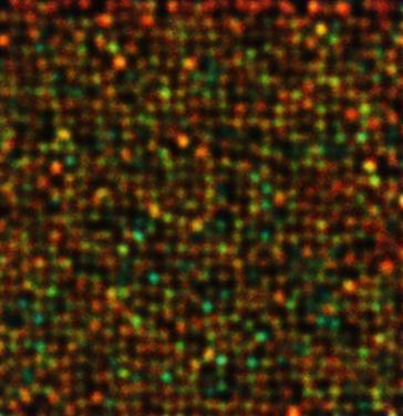
9 DARK FIELD OPTICAL MICROSCOPY OF DEWETTED SURFACES


10 DARK FIELD SPECTROSCOPY DARK FIELD MICROSCOPY OF INDIVIDUAL Si ISLANDS ATOMIC FORCE MICROSCOPY EXPERIMENT FEM SIMULATION ABBARCHI ACS nano 2014


11 ABBARCHI ACS nano 2014 SPONTANEOUS DEWETTING vs ASSISTED DEWETTING ANNEALING INDEPENDENT FROM SAMPLE SIZE!! TIME, TEMPERATURE E-BEAM AND RIE+ ANNEALING CONTROL OF SIZE AND SPACING
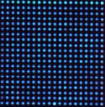
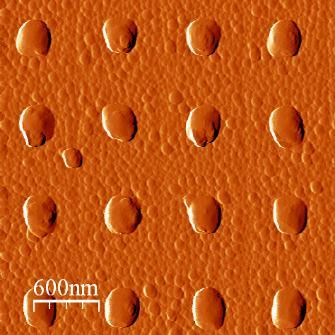
12 ASSISTED DEWETTING: FOCUSED ION BEAM 500 nm 750 nm 1000 nm ISLANDS SIZE
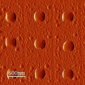
13 ASSISTED DEWETTING: FOCUSED ION BEAM LOW TEMPERATURE ANNEALING (SLOW DEWETTING REGIME): INDIVIDUAL MIE RESONATORS


14 FOCUSED ION BEAM + LOW TEMPERATURE DEWETTING: INDIVIDUAL RESONATOR ABBARCHI ACS nano 2014 ISHIKAWA, Appl. Surf. Sci.2002 MD ED MQ??
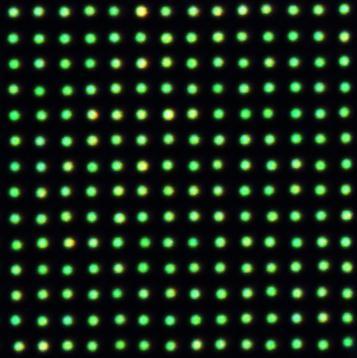
15 ASSISTED DEWETTING: FOCUSED ION BEAM HIGH TEMPERATURE ANNEALING (FAST DEWETTING REGIME): MIE RESONATOR OLIGOMERS
16 FOCUSED ION BEAM+HIGH TEMPERATURE DEWETTING: MIE RESONATORS OLIGOMERS ABBARCHI ACS nano 2014


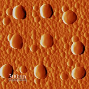
17 FOCUSED ION BEAM+DEWETTING + Ge DEPOSITION: MIE RESONATORS OLIGOMERS Ge deposition induces the collapse of the islands number IB PATTERN

18 FOCUSED ION BEAM+DEWETTING + Ge DEPOSITION:MIE RESONATORS OLIGOMERS


19 MIE RESONATORS OLIGOMERS: size and position distributions Silicon Silicon-germanium Silicon-germanium 3 mm


20 CONCLUSION: DEWETTING IS A RELEVANT FABRICATION METHOD FOR DIELECTRIC RESONATORS -PERFECTLY CRYSTALLINE ISLANDS WITH ATOMIC SMOOTH SURFACES -ONE STEP FABRICATION PROCESS, INDEPENDENT FROM THE SAMPLE SIZE!! -ALLOWS FOR A PRECISE CONTROL OF THE RESONATOR NUMBER -ELECTRIC CONTROL IS POSSIBLE


21 Meher Naffouti Thomas David THANK YOU!
NFO-School PROGRAM - Sunday August 26 UTT Room N101
 PROGRAM - Sunday August 26 UTT Room N101 8:45 WELCOME Lukas NOVOTNY, ETH Zurich, Switzerland. 9:00-10:30 Nicolas BONOD, CNRS, Institut Fresnel, Marseille, France. 20 Min Coffee Break Resonant Interaction
Wednesday 3 September Session 3: Metamaterials Theory (16:15 16:45, Huxley LT308)
") Session 3: Metamaterials Theory (16:15 16:45, Huxley LT308) (invited) TBC Session 3: Metamaterials Theory (16:45 17:00, Huxley LT308) Light trapping states in media with longitudinal electric waves D McArthur,
Session 3: Metamaterials Theory (16:15 16:45, Huxley LT308) (invited) TBC Session 3: Metamaterials Theory (16:45 17:00, Huxley LT308) Light trapping states in media with longitudinal electric waves D McArthur,
Laser-synthesized oxide-passivated bright Si quantum dots for bioimaging
 Supplementary Information to Laser-synthesized oxide-passivated bright Si quantum dots for bioimaging M. B. Gongalsky 1, L.A. Osminkina 1,2, A. Pereira 3, A. A. Manankov 1, A. A. Fedorenko 1, A. N. Vasiliev
Oscillateur paramétrique optique en
 C. Ozanam 1, X. Lafosse 2, I. Favero 1, S. Ducci 1, G. Leo 1 1 Université Paris Diderot, Sorbonne Paris Cité, Laboratoire MPQ, CNRS-UMR 7162, Paris, France, 2 Laboratoire de Photonique et Nanostructures,
Photonic Crystal Nanocavities for Efficient Light Confinement and Emission
 Journal of the Korean Physical Society, Vol. 42, No., February 2003, pp. 768 773 Photonic Crystal Nanocavities for Efficient Light Confinement and Emission Axel Scherer, T. Yoshie, M. Lončar, J. Vučković
High efficiency solar cells by nanophotonic design
 High efficiency solar cells by nanophotonic design Piero Spinelli Claire van Lare Jorik van de Groep Bonna Newman Mark Knight Paula Bronsveld Frank Lenzmann Ruud Schropp Wim Sinke Albert Polman Center
Wafer Scale Formation of Monocrystalline Silicon-Based Mie Resonators via Silicon-on-Insulator Dewetting
 Wafer Scale Formation of Monocrystalline Silicon-Based Mie Resonators via Silicon-on-Insulator Dewetting Marco Abbarchi,*, Meher Naffouti,, Benjamin Vial, Abdelmalek Benkouider, Laurent Lermusiaux, Luc
GeSi Quantum Dot Superlattices
 GeSi Quantum Dot Superlattices ECE440 Nanoelectronics Zheng Yang Department of Electrical & Computer Engineering University of Illinois at Chicago Nanostructures & Dimensionality Bulk Quantum Walls Quantum
Photonic Micro and Nanoresonators
 Photonic Micro and Nanoresonators Hauptseminar Nanooptics and Nanophotonics IHFG Stuttgart Overview 2 I. Motivation II. Cavity properties and species III. Physics in coupled systems Cavity QED Strong and
Nanomaterials and their Optical Applications
 Nanomaterials and their Optical Applications Winter Semester 2012 Lecture 08 rachel.grange@uni-jena.de http://www.iap.uni-jena.de/multiphoton Outline: Photonic crystals 2 1. Photonic crystals vs electronic
Crystalline Surfaces for Laser Metrology
 Crystalline Surfaces for Laser Metrology A.V. Latyshev, Institute of Semiconductor Physics SB RAS, Novosibirsk, Russia Abstract: The number of methodological recommendations has been pronounced to describe
Seminars in Nanosystems - I
 Seminars in Nanosystems - I Winter Semester 2011/2012 Dr. Emanuela Margapoti Emanuela.Margapoti@wsi.tum.de Dr. Gregor Koblmüller Gregor.Koblmueller@wsi.tum.de Seminar Room at ZNN 1 floor Topics of the
Nanojet and Surface Enhanced Raman Spectroscopy (NASERS) for Highly Reproducible and Controllable Single Molecule Detection
 for Highly Reproducible and Controllable Single Molecule Detection") Nanojet and Surface Enhanced Raman Spectroscopy (NASERS) for Highly Reproducible and Controllable Single Molecule Detection Te-Wei Chang, Manas Ranjan Gartia and Gang Logan Liu Department of Electrical
Nanojet and Surface Enhanced Raman Spectroscopy (NASERS) for Highly Reproducible and Controllable Single Molecule Detection Te-Wei Chang, Manas Ranjan Gartia and Gang Logan Liu Department of Electrical
Photonics Beyond Diffraction Limit:
 Photonics Beyond Diffraction Limit: Plasmon Cavity, Waveguide and Lasers Xiang Zhang University of California, Berkeley Light-Matter Interaction: Electrons and Photons Photons Visible / IR ~ 1 m Electrons
Nanocomposite photonic crystal devices
 Nanocomposite photonic crystal devices Xiaoyong Hu, Cuicui Lu, Yulan Fu, Yu Zhu, Yingbo Zhang, Hong Yang, Qihuang Gong Department of Physics, Peking University, Beijing, P. R. China Contents Motivation
Light Trapping on Plasmonic-Photonic Nanostructured Fluorine- Doped Tin Oxide
 pubs.acs.org/jpcc Light Trapping on Plasmonic-Photonic Nanostructured Fluorine- Doped Tin Oxide Fengli Wang, Qian Wang, Guowei Xu, Rongqing Hui, and Judy Wu* The University of Kansas, Lawrence, Kansas
Supporting file. Pulse Laser Induced Size-controllable and Symmetrical Ordering of Single Crystal Si
 Electronic Supplementary Material (ESI) for Nanoscale. This journal is The Royal Society of Chemistry 2018 Supporting file Pulse Laser Induced Size-controllable and Symmetrical Ordering of Single Crystal
Laser matter interaction
 Laser matter interaction PH413 Lasers & Photonics Lecture 26 Why study laser matter interaction? Fundamental physics Chemical analysis Material processing Biomedical applications Deposition of novel structures
Nanomaterials and their Optical Applications
 Nanomaterials and their Optical Applications Winter Semester 2013 Lecture 02 rachel.grange@uni-jena.de http://www.iap.uni-jena.de/multiphoton Lecture 2: outline 2 Introduction to Nanophotonics Theoretical
Supplementary Information. Light Manipulation for Organic Optoelectronics Using Bio-inspired Moth's Eye. Nanostructures
 Supplementary Information Light Manipulation for Organic Optoelectronics Using Bio-inspired Moth's Eye Nanostructures Lei Zhou, Qing-Dong Ou, Jing-De Chen, Su Shen, Jian-Xin Tang,* Yan-Qing Li,* and Shuit-Tong
The fabrication of periodic metal nanodot arrays through pulsed laser melting induced fragmentation of metal nanogratings
 IOP PUBLISHING Nanotechnology 20 (2009) 285310 (5pp) NANOTECHNOLOGY doi:10.1088/0957-4484/20/28/285310 The fabrication of periodic metal nanodot arrays through pulsed laser melting induced fragmentation
Nanostrukturphysik (Nanostructure Physics)
") Nanostrukturphysik (Nanostructure Physics) Prof. Yong Lei & Dr. Yang Xu Fachgebiet 3D-Nanostrukturierung, Institut für Physik Contact: yong.lei@tu-ilmenau.de; yang.xu@tu-ilmenau.de Office: Unterpoerlitzer
Nanostrukturphysik (Nanostructure Physics) Prof. Yong Lei & Dr. Yang Xu Fachgebiet 3D-Nanostrukturierung, Institut für Physik Contact: yong.lei@tu-ilmenau.de; yang.xu@tu-ilmenau.de Office: Unterpoerlitzer
NANOCOMPOSITE THIN FILMS:
 NANOCOMPOSITE THIN FILMS: Assembly, Characterizations, & Applications Chaoyang Jiang Department of Chemistry The University of South Dakota St. Louis, June 26, 2008 Forest Products &Nanocomposite P. Monteiro@UC
Nanophysics: Main trends
 Nano-opto-electronics Nanophysics: Main trends Nanomechanics Main issues Light interaction with small structures Molecules Nanoparticles (semiconductor and metallic) Microparticles Photonic crystals Nanoplasmonics
Nanostructure. Materials Growth Characterization Fabrication. More see Waser, chapter 2
 Nanostructure Materials Growth Characterization Fabrication More see Waser, chapter 2 Materials growth - deposition deposition gas solid Physical Vapor Deposition Chemical Vapor Deposition Physical Vapor
EPSILON-NEAR-ZERO (ENZ) AND MU-NEAR-ZERO (MNZ) MATERIALS
 AND MU-NEAR-ZERO (MNZ) MATERIALS") EPSILON-NEAR-ZERO (ENZ) AND MU-NEAR-ZERO (MNZ) MATERIALS SARAH NAHAR CHOWDHURY PURDUE UNIVERSITY 1 Basics Design ENZ Materials Lumped circuit elements Basics Decoupling Direction emission Tunneling Basics
EPSILON-NEAR-ZERO (ENZ) AND MU-NEAR-ZERO (MNZ) MATERIALS SARAH NAHAR CHOWDHURY PURDUE UNIVERSITY 1 Basics Design ENZ Materials Lumped circuit elements Basics Decoupling Direction emission Tunneling Basics
Fabrication of microcraters on silicon substrate by UV nanosecond photonic nanojets from microspheres
 UVX 2012, 02003 (2013) DOI: 10.1051/uvx/201302003 C Owned by the authors, published by EDP Sciences, 2013 Fabrication of microcraters on silicon substrate by UV nanosecond photonic nanojets from microspheres
Revealing High Fidelity of Nanomolding Process by Extracting the Information from AFM Image with Systematic Artifacts
 Revealing High Fidelity of Nanomolding Process by Extracting the Information from AFM Image with Systematic Artifacts Sajal Biring* Department of Electronics Engineering and Organic Electronics Research
Resonator Fabrication for Cavity Enhanced, Tunable Si/Ge Quantum Cascade Detectors
 Resonator Fabrication for Cavity Enhanced, Tunable Si/Ge Quantum Cascade Detectors M. Grydlik 1, P. Rauter 1, T. Fromherz 1, G. Bauer 1, L. Diehl 2, C. Falub 2, G. Dehlinger 2, H. Sigg 2, D. Grützmacher
PLASMONICS/METAMATERIALS
 PLASMONICS/METAMATERIALS Interconnects Optical processing of data Subwavelength confinement Electrodes are in place Coupling to other on-chip devices Combination of guiding, detection, modulation, sensing
arxiv: v1 [physics.optics] 12 Dec 2015
![arxiv: v1 [physics.optics] 12 Dec 2015](/thumbs/94/119526498.jpg "arxiv: v1 [physics.optics] 12 Dec 2015") Laser fabrication of crystalline silicon nanoresonators from an amorphous film for low-loss all-dielectric nanophotonics P. A. Dmitriev, 1 S. V. Makarov, 1 V. A. Milichko, 1 I. S. Mukhin, 1,2 A. S. Gudovskikh,
Laser fabrication of crystalline silicon nanoresonators from an amorphous film for low-loss all-dielectric nanophotonics P. A. Dmitriev, 1 S. V. Makarov, 1 V. A. Milichko, 1 I. S. Mukhin, 1,2 A. S. Gudovskikh,
Micro- and Nano-Technology... for Optics
 Micro- and Nano-Technology...... for Optics U.D. Zeitner Fraunhofer Institut für Angewandte Optik und Feinmechanik Jena Today: 1. Introduction E. Bernhard Kley Institute of Applied Physics Friedrich-Schiller
Optics of complex micro structures
 Optics of complex micro structures dielectric materials λ L disordered partially ordered ordered random multiple scattering liquid crystals quasi crystals (Fibonacci) photonic crystals Assembly of photonic
Fabrication and optical measurements of silicon on insulator photonic nanostructures
 Microelectronic Engineering 61 62 (2002) 529 536 www.elsevier.com/ locate/ mee Fabrication and optical measurements of silicon on insulator photonic nanostructures * M. Agio, L.C. Andreani, E. Silberstein,
Song Fengqi, Zhang Lu, Zhu Lianzhong, Ge Jun, Wang Guanghou *
 Low energy cluster beam deposited BN films as the cascade for Field Emission 一 Song Fengqi, Zhang Lu, Zhu Lianzhong, Ge Jun, Wang Guanghou * National laboratory of Solid State Microstructures, Department
Südliche Stadtmauerstr. 15a Tel: D Erlangen Fax:
 Curriculum Vitae Lionel Santinacci 19.10.1974 Nationality: French Südliche Stadtmauerstr. 15a Tel: + 49 9131 852 7587 D-91054 Erlangen Fax: + 49 9131 852 7582 Germany e-mail: lionel@ww.uni-erlangen.de
Very large plasmon band shift in strongly coupled metal nanoparticle chain arrays.
 Mat. Res. Soc. Symp. Proc. Vol. 797 2004 Materials Research Society W4.6.1 Very large plasmon band shift in strongly coupled metal nanoparticle chain arrays. L. A. Sweatlock 1, J. J. Penninkhof 2, S. A.
NSF EPSCoR Kansas Center for Solar Energy Research Annual Program Review June 12-14, 2011
 NSF EPSCoR Kansas Center for Solar Energy Research Annual Program Review June 12-14, 2011 Plasmonic and Photonic Photovoltaics based on graphene and other carbon nanostructures Fengli Wang, Guowei Xu,
The Photonic Band Gap and Colloidal Crystals. Focus: Photonic Band Gap
 The Photonic Band Gap and Colloidal Crystals David J. Norris Chemical Engineering & Materials Science University of Minnesota Focus: Photonic Band Gap What is it? Why is it interesting? How do colloidal
Large-Area and Uniform Surface-Enhanced Raman. Saturation
 Supporting Information Large-Area and Uniform Surface-Enhanced Raman Spectroscopy Substrate Optimized by Enhancement Saturation Daejong Yang 1, Hyunjun Cho 2, Sukmo Koo 1, Sagar R. Vaidyanathan 2, Kelly
Supplementary Figure S1 Anticrossing and mode exchange between D1 (Wood's anomaly)
") Supplementary Figure S1 Anticrossing and mode exchange between D1 (Wood's anomaly) and D3 (Fabry Pérot cavity mode). (a) Schematic (top) showing the reflectance measurement geometry and simulated angle-resolved
Supplementary Figure S1 Anticrossing and mode exchange between D1 (Wood's anomaly) and D3 (Fabry Pérot cavity mode). (a) Schematic (top) showing the reflectance measurement geometry and simulated angle-resolved
Surface plasmon resonance based refractive index sensor for liquids
 Indian Journal of Pure & Applied Physics Vol. 43, November 005, pp. 854-858 Surface plasmon resonance based refractive index sensor for liquids Navina Mehan, Vinay Gupta, K Sreenivas & Abhai Mansingh Department
Nova 600 NanoLab Dual beam Focused Ion Beam IITKanpur
 Nova 600 NanoLab Dual beam Focused Ion Beam system @ IITKanpur Dual Beam Nova 600 Nano Lab From FEI company (Dual Beam = SEM + FIB) SEM: The Electron Beam for SEM Field Emission Electron Gun Energy : 500
Terahertz antireflection coating enabled by a subwavelength metallic mesh capped with a thin dielectric film
 Invited Paper Terahertz antireflection coating enabled by a subwavelength metallic mesh capped with a thin dielectric film Li Huang 1*, Beibei Zeng 2, Chun-Chieh Chang 2 and Hou-Tong Chen 2* 1 Physics
Some Topics in Optics
 Some Topics in Optics The HeNe LASER The index of refraction and dispersion Interference The Michelson Interferometer Diffraction Wavemeter Fabry-Pérot Etalon and Interferometer The Helium Neon LASER A
A Study on the Suitability of Indium Nitride for Terahertz Plasmonics
 A Study on the Suitability of Indium Nitride for Terahertz Plasmonics Arjun Shetty 1*, K. J. Vinoy 1, S. B. Krupanidhi 2 1 Electrical Communication Engineering, Indian Institute of Science, Bangalore,
JOHN G. EKERDT RESEARCH FOCUS
 JOHN G. EKERDT RESEARCH FOCUS We study the surface, growth and materials chemistry of metal, dielectric, ferroelectric, and polymer thin films. We seek to understand and describe nucleation and growth
Ion Beam radiation and temperature effect on Co/Si and CoO/Co/Si thin films
 M (emu) Ion Beam radiation and temperature effect on Co/Si and CoO/Co/Si thin films A.S.Bhattacharyya Centre for Nanotechnology Central University of Jharkhand Brambe, Ranchi: 835205 Email: 2006asb@gmail.com
Quantum optics of many-body systems
 Quantum optics of many-body systems Igor Mekhov Université Paris-Saclay (SPEC CEA) University of Oxford, St. Petersburg State University Lecture 2 Previous lecture 1 Classical optics light waves material
1) Institut d Electronique Fondamentale, CNRS, Univ. Paris- Sud, Université Paris- Saclay, Bâtiment 220, Rue André Ampère, F Orsay, France
 Institut d Electronique Fondamentale, CNRS, Univ. Paris- Sud, Université Paris- Saclay, Bâtiment 220, Rue André Ampère, F Orsay, France") Supporting information Direct band gap germanium microdisks obtained with silicon nitride stressor layers Moustafa El Kurdi, 1 Mathias Prost, 1 Abdelhamid Ghrib, 1 Sébastien Sauvage, 1 Xavier Checoury,
Supporting information Direct band gap germanium microdisks obtained with silicon nitride stressor layers Moustafa El Kurdi, 1 Mathias Prost, 1 Abdelhamid Ghrib, 1 Sébastien Sauvage, 1 Xavier Checoury,
Ultrafast surface carrier dynamics in topological insulators: Bi 2 Te 3. Marino Marsi
 Ultrafast surface carrier dynamics in topological insulators: Bi 2 Te 3 Marino Marsi Laboratoire de Physique des Solides CNRS UMR 8502 - Université Paris-Sud IMPACT, Orsay, September 2012 Outline Topological
Fano-Resonance Photonic Crystal Membrane Reflectors at Mid- and Far-Infrared
 Fano-Resonance Photonic Crystal Membrane Reflectors at Mid- and Far-Infrared Volume 5, Number 1, February 2013 Yichen Shuai Deyin Zhao Gautam Medhi Robert Peale Zhenqiang Ma, Member, IEEE Walter Buchwald
Light Interaction with Small Structures
 Light Interaction with Small Structures Molecules Light scattering due to harmonically driven dipole oscillator Nanoparticles Insulators Rayleigh Scattering (blue sky) Semiconductors...Resonance absorption
Gaetano L Episcopo. Scanning Electron Microscopy Focus Ion Beam and. Pulsed Plasma Deposition
 Gaetano L Episcopo Scanning Electron Microscopy Focus Ion Beam and Pulsed Plasma Deposition Hystorical background Scientific discoveries 1897: J. Thomson discovers the electron. 1924: L. de Broglie propose
Lecture 10: Surface Plasmon Excitation. 5 nm
 Excitation Lecture 10: Surface Plasmon Excitation 5 nm Summary The dispersion relation for surface plasmons Useful for describing plasmon excitation & propagation This lecture: p sp Coupling light to surface
Fabrication at the nanoscale for nanophotonics
 Fabrication at the nanoscale for nanophotonics Ilya Sychugov, KTH Materials Physics, Kista silicon nanocrystal by electron beam induced deposition lithography Outline of basic nanofabrication methods Devices
Elements of Quantum Optics
 Pierre Meystre Murray Sargent III Elements of Quantum Optics Fourth Edition With 124 Figures fya Springer Contents 1 Classical Electromagnetic Fields 1 1.1 Maxwell's Equations in a Vacuum 2 1.2 Maxwell's
Sub-wavelength electromagnetic structures
 Sub-wavelength electromagnetic structures Shanhui Fan, Z. Ruan, L. Verselegers, P. Catrysse, Z. Yu, J. Shin, J. T. Shen, G. Veronis Ginzton Laboratory, Stanford University http://www.stanford.edu/group/fan
Hong-Ou-Mandel effect with matter waves
 Hong-Ou-Mandel effect with matter waves R. Lopes, A. Imanaliev, A. Aspect, M. Cheneau, DB, C. I. Westbrook Laboratoire Charles Fabry, Institut d Optique, CNRS, Univ Paris-Sud Progresses in quantum information
arxiv: v2 [physics.optics] 14 Dec 2017
![arxiv: v2 [physics.optics] 14 Dec 2017](/thumbs/90/104342510.jpg "arxiv: v2 [physics.optics] 14 Dec 2017") All-dielectric nanophotonics: fundamentals, fabrication, and applications Alexander Krasnok a,b,, Roman Savelev b, Denis Baranov c,d, and Pavel Belov b a The University of Texas at Austin, Austin, Texas
All-dielectric nanophotonics: fundamentals, fabrication, and applications Alexander Krasnok a,b,, Roman Savelev b, Denis Baranov c,d, and Pavel Belov b a The University of Texas at Austin, Austin, Texas
Graphene for THz technology
 Graphene for THz technology J. Mangeney1, J. Maysonnave1, S. Huppert1, F. Wang1, S. Maero1, C. Berger2,3, W. de Heer2, T.B. Norris4, L.A. De Vaulchier1, S. Dhillon1, J. Tignon1 and R. Ferreira1 1 Laboratoire
Abnormal PL spectrum in InGaN MQW surface emitting cavity
 Abnormal PL spectrum in InGaN MQW surface emitting cavity J. T. Chu a, Y.-J. Cheng b, H. C. Kuo a, T. C. Lu a, and S. C. Wang a a Department of Photonics & Institute of Electro-Optical Engineering, National
Strong Coupling between On Chip Notched Ring Resonator and Nanoparticle
 Strong Coupling between On Chip Notched Ring Resonator and Nanoparticle S. Wang 1, K. Broderick 1, 3, H. Smith 1 2, 3,1 *, and Y. Yi 1 Massauchusetts Institute of Technology, Cambridge, MA 02139 2 New
Polarization control of defect modes in threedimensional woodpile photonic crystals
 Polarization control of defect modes in threedimensional woodpile photonic crystals Michael James Ventura and Min Gu* Centre for Micro-Photonics and Centre for Ultrahigh-bandwidth Devices for Optical Systems,
Semiconductor Disk Laser on Microchannel Cooler
 Semiconductor Disk Laser on Microchannel Cooler Eckart Gerster An optically pumped semiconductor disk laser with a double-band Bragg reflector mirror is presented. This mirror not only reflects the laser
Optics, Light and Lasers
 Dieter Meschede Optics, Light and Lasers The Practical Approach to Modern Aspects of Photonics and Laser Physics Second, Revised and Enlarged Edition BICENTENNIAL.... n 4 '':- t' 1 8 0 7 $W1LEY 2007 tri
Micro-patterned porous silicon using proton beam writing
 Micro-patterned porous silicon using proton beam writing M. B. H. Breese, D. Mangaiyarkarasi, E. J. Teo*, A. A. Bettiol and D. Blackwood* Centre for Ion Beam Applications, Department of Physics, National
Electronic States of Nanocrystal Doped with Oxygen and Visible Emission on Black Silicon Prepared by ns-laser
 Huang et al. Nanoscale Research Letters (2017) 12:452 DOI 10.1186/s11671-017-2209-3 NANO EXPRESS Electronic States of Nanocrystal Doped with Oxygen and Visible Emission on Black Silicon Prepared by ns-laser
Computational Optoelectronics Group, Integrated Systems Laboratory, ETH Zurich 2. Institute of Photonics and Quantum Electronics, EPF Lausanne
 Modelling the Purcell Effect in Photonic Crystal Cavities with a 3D Finite Element Maxwell Solver Friedhard Römer 1, Andrea Fiore 2, Laurent Balet 2, and Bernd Witzigmann 1 1 Computational Optoelectronics
Nano fabrication and optical characterization of nanostructures
 Introduction to nanooptics, Summer Term 2012, Abbe School of Photonics, FSU Jena, Prof. Thomas Pertsch Nano fabrication and optical characterization of nanostructures Lecture 12 1 Optical characterization
Plasmon enhanced UV electroluminescence in SiO 2 with percolating conduction sustained by free-exciton emitting SnO 2 nanoparticles
 Dipartimento di Scienza dei Materiali Università di Milano-Bicocca TITLE Plasmon enhanced UV electroluminescence in O 2 with percolating conduction sustained by free-exciton emitting SnO 2 nanoparticles
Current issues in coherence for small laser sources
 Current issues in coherence for small laser sources G.L. Lippi Institut Non Linéaire de Nice Université de Nice-Sophia Antipolis and UMR 7335 CNRS with the support of : P.1 Coworkers At the INLN Experiments
2D Materials Research Activities at the NEST lab in Pisa, Italy. Stefan Heun NEST, Istituto Nanoscienze-CNR and Scuola Normale Superiore, Pisa, Italy
 2D Materials Research Activities at the NEST lab in Pisa, Italy Stefan Heun NEST, Istituto Nanoscienze-CNR and Scuola Normale Superiore, Pisa, Italy 2D Materials Research Activities at the NEST lab in
Fundamentals of Nanoelectronics: Basic Concepts
 Fundamentals of Nanoelectronics: Basic Concepts Sławomir Prucnal FWIM Page 1 Introduction Outline Electronics in nanoscale Transport Ohms law Optoelectronic properties of semiconductors Optics in nanoscale
U-Shaped Nano-Apertures for Enhanced Optical Transmission and Resolution
 U-Shaped Nano-Apertures for Enhanced Optical Transmission and Resolution Mustafa Turkmen 1,2,3, Serap Aksu 3,4, A. Engin Çetin 2,3, Ahmet A. Yanik 2,3, Alp Artar 2,3, Hatice Altug 2,3,4, * 1 Electrical
Highly Sensitive Color-Tunablility by Scalable. Nanomorphology of Dielectric Layer in Liquid Permeable. Metal-Insulator-Metal Structure
 Supporting Information Highly Sensitive Color-Tunablility by Scalable Nanomorphology of Dielectric Layer in Liquid Permeable Metal-Insulator-Metal Structure Eui-Sang Yu,, Sin-Hyung Lee, Young-Gyu Bae,
Towards the Lasing Spaser: Controlling. Metamaterial Optical Response with Semiconductor. Quantum Dots
 Towards the Lasing Spaser: Controlling Metamaterial Optical Response with Semiconductor Quantum Dots E. Plum, V. A. Fedotov, P. Kuo, D. P. Tsai, and N. I. Zheludev,, Optoelectronics Research Centre, University
DIELECTRIC nanoparticles (NPs) have recently been proposed
 have recently been proposed") IEEE JOURNAL OF PHOTOVOLTAICS 1 Effect of EVA Encapsulation on Antireflection Properties of Mie Nanoscatterers for c-si Solar Cells P. Spinelli, F. Lenzmann, A. Weeber, and A. Polman Abstract Dielectric
IEEE JOURNAL OF PHOTOVOLTAICS 1 Effect of EVA Encapsulation on Antireflection Properties of Mie Nanoscatterers for c-si Solar Cells P. Spinelli, F. Lenzmann, A. Weeber, and A. Polman Abstract Dielectric
Optimizing Graphene Morphology on SiC(0001)
") Optimizing Graphene Morphology on SiC(0001) James B. Hannon Rudolf M. Tromp Graphene sheets Graphene sheets can be formed into 0D,1D, 2D, and 3D structures Chemically inert Intrinsically high carrier mobility
Optimizing Graphene Morphology on SiC(0001) James B. Hannon Rudolf M. Tromp Graphene sheets Graphene sheets can be formed into 0D,1D, 2D, and 3D structures Chemically inert Intrinsically high carrier mobility
Quantum coherence in semiconductor nanostructures. Jacqueline Bloch
 Quantum coherence in semiconductor nanostructures Jacqueline Bloch Laboratoire of Photonic and Nanostructures LPN/CNRS Marcoussis Jacqueline.bloch@lpn.cnrs.fr Laboratoire de Photonique et de Nanostructures
Three Approaches for Nanopatterning
 Three Approaches for Nanopatterning Lithography allows the design of arbitrary pattern geometry but maybe high cost and low throughput Self-Assembly offers high throughput and low cost but limited selections
(Co-PIs-Mark Brongersma, Yi Cui, Shanhui Fan) Stanford University. GCEP Research Symposium 2013 Stanford, CA October 9, 2013
 Stanford University. GCEP Research Symposium 2013 Stanford, CA October 9, 2013") High-efficiency thin film nano-structured multi-junction solar James S. cells Harris (PI) (Co-PIs-Mark Brongersma, Yi Cui, Shanhui Fan) Stanford University GCEP Research Symposium 2013 Stanford, CA October
High-efficiency thin film nano-structured multi-junction solar James S. cells Harris (PI) (Co-PIs-Mark Brongersma, Yi Cui, Shanhui Fan) Stanford University GCEP Research Symposium 2013 Stanford, CA October
Nanophotonics: solar and thermal applications
 Nanophotonics: solar and thermal applications Shanhui Fan Ginzton Laboratory and Department of Electrical Engineering Stanford University http://www.stanford.edu/~shanhui Nanophotonic Structures Photonic
Photon Energy Dependence of Contrast in Photoelectron Emission Microscopy of Si Devices
 Photon Energy Dependence of Contrast in Photoelectron Emission Microscopy of Si Devices V. W. Ballarotto, K. Siegrist, R. J. Phaneuf, and E. D. Williams University of Maryland and Laboratory for Physical
Plasmon Assisted Nd 3+ -Based Solid-State Nanolaser
 Supporting Information for Plasmon Assisted Nd 3+ -Based Solid-State Nanolaser Pablo Molina, 1 Eduardo Yraola, 1 Mariola O. Ramírez, 1 Christos Tserkezis, 2 José L. Plaza, 1 Javier Aizpurua, 2 Jorge Bravo-Abad
Polarization independent broadband reflectors based on cross-stacked gratings
 Polarization independent broadband reflectors based on cross-stacked gratings Deyin Zhao, Hongjun Yang, Zhenqiang Ma, and Weidong Zhou,* Department of Electrical Engineering, NanoFAB Center, University
Depth Distribution Functions of Secondary Electron Production and Emission
 Depth Distribution Functions of Secondary Electron Production and Emission Z.J. Ding*, Y.G. Li, R.G. Zeng, S.F. Mao, P. Zhang and Z.M. Zhang Hefei National Laboratory for Physical Sciences at Microscale
ENHANCEMENT OF PHOTONIC BAND GAP IN A DIS- ORDERED QUARTER-WAVE DIELECTRIC PHOTONIC CRYSTAL
 Progress In Electromagnetics Research, PIER, 27 36, 1 ENHANCEMENT OF PHOTONIC BAN GAP IN A IS- ORERE QUARTER-WAVE IELECTRIC PHOTONIC CRYSTAL C.-J. Wu, Y.-N. Rau, and W.-H. Han Institute of Electro-Optical
This document contains the following supporting information: 1. Wide field scanning electron microscope image
 Supporting information for Self-assembled nanoparticle dimer antennas for plasmonic-enhanced single-molecule fluorescence detection at micromolar concentrations Deep Punj, Raju Regmi, Alexis Devilez, Robin
Investigation on Mode Splitting and Degeneracy in the L3 Photonic Crystal Nanocavity via Unsymmetrical Displacement of Air-Holes
 The International Journal Of Engineering And Science (Ijes) Volume 2 Issue 2 Pages 146-150 2013 Issn: 2319 1813 Isbn: 2319 1805 Investigation on Mode Splitting and Degeneracy in the L3 Photonic Crystal
Supplementary Information
 Electronic Supplementary Material (ESI) for Nanoscale. This journal is The Royal Society of Chemistry 2014 Supplementary Information Large-scale lithography-free metasurface with spectrally tunable super
Light trapping in thin-film solar cells: the role of guided modes
 Light trapping in thin-film solar cells: the role of guided modes T. Søndergaard *, Y.-C. Tsao, T. G. Pedersen, and K. Pedersen Department of Physics and Nanotechnology, Aalborg University, Skjernvej 4A,
Micromachining structured optical fibres using focused ion. beam (FIB) milling
 milling") Micromachining structured optical fibres using focused ion beam (FIB) milling Cicero Martelli Optical Fibre Technology Centre, School of Chemistry, University of Sydney, 206 National Innovation Centre,
Micromachining structured optical fibres using focused ion beam (FIB) milling Cicero Martelli Optical Fibre Technology Centre, School of Chemistry, University of Sydney, 206 National Innovation Centre,
Dielectric-Band Photonic Crystal Nanobeam Lasers
 36 JOURNAL OF LIGHTWAVE TECHNOLOGY, VOL. 31, NO. 1, JANUARY 1, 2013 Dielectric-Band Photonic Crystal Nanobeam Lasers Po-Tsung Lee, Member, IEEE, Tsan-Wen Lu, and Li-Hsun Chiu Abstract We investigate a
Photonic crystal laser threshold analysis using 3D FDTD with a material gain model
 Photonic crystal laser threshold analysis using 3D FDTD with a material gain model Adam Mock and John O'Brien Microphotonic Device Group University of Southern California July 14, 2009 Session: ITuD6 Integrated
TUNABLE MULTI-CHANNEL FILTERING USING 1-D PHOTONIC QUANTUM WELL STRUCTURES
 Progress In Electromagnetics Research Letters, Vol. 27, 43 51, 2011 TUNABLE MULTI-CHANNEL FILTERING USING 1-D PHOTONIC QUANTUM WELL STRUCTURES B. Suthar * and A. Bhargava Nanophysics Laboratory, Department
Radiation-matter interaction.
 Radiation-matter interaction Radiation-matter interaction Classical dipoles Dipole radiation Power radiated by a classical dipole in an inhomogeneous environment The local density of optical states (LDOS)
Nonlinear evolution of the morphological instability of a strained epitaxial film
 Nonlinear evolution of the morphological instability of a strained epitaxial film Thomas Frisch, Jean-No Noël Aqua, Alberto Verga, IM2NP,Marseille 1. Self-organization and crystal growth (step dynamics)
Advanced Workshop on Nanomechanics September Optomechanics with micro and nano-mirrors
 2445-09 Advanced Workshop on Nanomechanics 9-13 September 2013 Optomechanics with micro and nano-mirrors Samuel Deléglise Laboratoire Kastler Brossel Universite P. et M. Curie Optomechanics with micro
Multiple Fano Resonances Structure for Terahertz Applications
 Progress In Electromagnetics Research Letters, Vol. 50, 1 6, 2014 Multiple Fano Resonances Structure for Terahertz Applications Hadi Amarloo *, Daniel M. Hailu, and Safieddin Safavi-Naeini Abstract A new