Printing Silver Nanogrids on Glass: A Hands-on Investigation of Transparent Conductive Electrodes
|
|
|
- Melvin Tucker
- 6 years ago
- Views:
Transcription

1 Printing Silver Nanogrids on Glass: A Hands-on Investigation of Transparent Conductive Electrodes

2 Silver Nanogrid/Nanowire Importance The next generation of optoelectronic devices requires transparent conductive electrodes to be lightweight, flexible, cheap, and compatible with large scale manufacturing methods. Kumar, A,. Zhou, C.; The Race to Replace Tin-Doped Indium Oxide: Which Material Will Win? ACS Nano, 4,
 (PVP) and copper(ii) chloride.")

3 Silver Nanowire Synthesis Polyol Method: Silver nitrate is reduced by ethylene glycol in the presence of poly(vinylpyrrolidone) (PVP) and copper(ii) chloride. PVP acts as a stabilizing agent, while the copper chloride likely controls the rate of silver reduction and initial seed formation. Korte, K. Rapid Synthesis of Silver Nanowires NNIN REU Program, Seattle, WA, 2007;


4 Silver Nanowire Synthesis Template-Assisted Nanowire Synthesis Bentley, A. K.; Farhoud, A. B.; Ellis, A. B.; Lisensky, G. C.; Crone, W. C. J. Template Synthesis and Magnetic Manipulation of Nickel Nanowires. J. Chem. Educ. 2005, 82,
5 Objectives 1. To provide a simple and low-cost experiment that allows introductory nanotechnology students to become familiar with micro- and nanofabrication (direct-printing methods) with real-world relevance. 2. To provide students with opportunities to use various characterization techniques. 3. To introduce students to template modification.
6 Associated Labs Microcontact-Printing of PVP Grid ENGR 1050: Introduction to Nanotechnology Conductive AFM MSE 2320: Introduction to Scanning Probe Microscopy Bright-Field Microscopy MSE 1820: Fundamentals of Microscopy


7 Publication Sanders. W. C.; Fabrication of Polyvinylpyrrolidone Micro-/Nanostructures Utilizing Microcontact Printing. J. Chem. Ed. 2015, 92,


8 Publication Sanders. W. C., Valcarce, R., Iles, P., Smith, J. S.; Glass, G., Gomez, J., Johnson, G., Johnston, D., Morham, M., Beefus, E., Oz, A., Tomaraei, M.; Printing Silver Nanogrids on Glass. J. Chem. Ed. 2017, 94,

9 Soft Lithography Soft organic materials are used to transfer patterns to substrates. Conformal contact: Stamp is elastic enough to conform to the substrate.


10 Preparing PDMS Stamps 10 g of silicone elastomer 0.9 g of curing agent Mix for one minute

11 Microcontact Printing Master AFM image of compact disk.


12 Preparing PDMS Stamps 1. Cut a CD square 5. Remove stamp from dish 3. Place CD in a shallow dish 2. Remove labels *PDMS is cured on a hot plate for minutes 4. Pour PDMS over CD*
13 Polyvinylpyrrolidone Binder in many pharmaceutical tablets. Adhesive in glue and hot-melt sticks. Used to increase the solubility of drugs in liquid and semi-liquid forms. Found in personal care products (shampoos, toothpastes) and paints.
14 PVP/Silver Ion Interactions M + M + M + PVP has a strong tendency for complex formation with small molecules and readily interacts with metal cations in solution. Khan, M. S.; Gul, K.; Rehman, N. U. Interaction of Polyvinylpyrrolidone with Metal Chloride Aqueous Solutions. Chin. J. Polym. Sci. 2004, 22,


15 Challenge 1: PDMS/Solution Interaction Water on PDMS Alcohol on PDMS PVP is soluble in water and various alcohols.

 Fibers: Effects of")
16 Challenge 2: Humidity Small amounts of water can result in the formation of beaded PVP structures. Yuya, N.; Kai, W.; Kim, B. S.; Kim, I. S. Morphology Controlled Electrospun Poly(vinylpyrrolidone) Fibers: Effects of Organic Solid and Relative Humidity. J. Mat. Sci. Eng. with Adv. Tech., 2010, 2,
 Fibers: Effects of Organic Solid and Relative Humidity. J. Mat. Sci. Eng.")
17 Challenge 2: Humidity The presence of water can also result in the formation of PVP films. Yuya, N.; Kai, W.; Kim, B. S.; Kim, I. S. Morphology Controlled Electrospun Poly(vinylpyrrolidone) Fibers: Effects of Organic Solid and Relative Humidity. J. Mat. Sci. Eng. with Adv. Tech., 2010, 2,


18 Challenge 2: Humidity Small traces of water on the surface of stamps and substrates is removed by heating with a hot plate for approximately 10 minutes prior to the experiment.

19 Procedure: Spin Coat PVP
20 Procedure: Microcontact-Printing
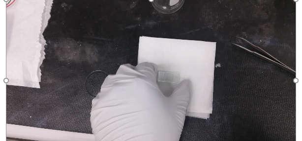
21 Procedure: Microcontact-Printing
22 Procedure: Microcontact-Printing
23 Procedure: Sputter Coating with Copper Comparison of cross-sectional data for a PVP grid with no copper layer, and for the same PVP grid after addition of the copper layer suggests the thickness of the copper layer is approximately 5 nanometers thick. Sanders. W. C., Valcarce, R., Iles, P., Smith, J. S.; Glass, G., Gomez, J., Johnson, G., Johnston, D., Morham, M., Beefus, E., Oz, A., Tomaraei, M.; Printing Silver Nanogrids on Glass. J. Chem. Ed. 2017, 94,
 + O 2(g) Ratyakshi; Chauhan, R. P. Colloidal Synthesis of Silver Nano Particles. Asian J. Chem. 2009, 21, S113-116.")
24 Procedures: Metallization 4 Ag + (aq)+ C 6 H 5 O 7 Na 3(aq) + 2 H 2 O (l) 4 Ag 0 (s) + C 6 H 5 O 7 H 3(aq) + 3 Na + (aq) + H + (aq) + O 2(g) Ratyakshi; Chauhan, R. P. Colloidal Synthesis of Silver Nano Particles. Asian J. Chem. 2009, 21, S

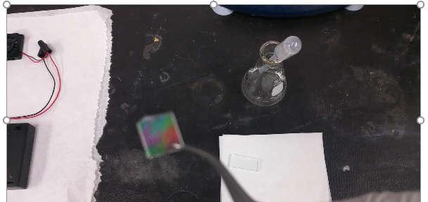
25 Silver Grid on Glass
")
26 Optical Images Optical microscope image of PVP grid (40x objective)

27 Optical Images Optical microscope image of silver grid (40x objective)
. Sanders. W. C., Valcarce, R., Iles, P., Smith, J. S.; Glass, G., Gomez, J., Johnson, G., Johnston, D., Morham, M., Beefus, E., Oz, A., Tomaraei, M.")
28 AFM Data: Physical Dimensions Atomic force microscope images of copper-coated PVP grid before the reaction with silver nitrate/sodium citrate solution (a) and after the reaction (b). A cross-sectional profile of both AFM scans (c). Sanders. W. C., Valcarce, R., Iles, P., Smith, J. S.; Glass, G., Gomez, J., Johnson, G., Johnston, D., Morham, M., Beefus, E., Oz, A., Tomaraei, M.; Printing Silver Nanogrids on Glass. J. Chem. Ed. 2017, 94,

29 SEM Data EDS scan on and off the silver nanogrid pattern (a). EDS spectra of both scans (b). Sanders. W. C., Valcarce, R., Iles, P., Smith, J. S.; Glass, G., Gomez, J., Johnson, G., Johnston, D., Morham, M., Beefus, E., Oz, A., Tomaraei, M.; Printing Silver Nanogrids on Glass. J. Chem. Ed. 2017, 94,


30 SEM Data Sanders. W. C., Valcarce, R., Iles, P., Smith, J. S.; Glass, G., Gomez, J., Johnson, G., Johnston, D., Morham, M., Beefus, E., Oz, A., Tomaraei, M.; Printing Silver Nanogrids on Glass. J. Chem. Ed. 2017, 94,

31 Conductivity Sanders. W. C., Valcarce, R., Iles, P., Smith, J. S.; Glass, G., Gomez, J., Johnson, G., Johnston, D., Morham, M., Beefus, E., Oz, A., Tomaraei, M.; Printing Silver Nanogrids on Glass. J. Chem. Ed. 2017, 94,
32 Acknowledgements SLCC Chemistry Department SLCC Engineering Department Dr. Peter Iles Ron Valcarce Dr. James Smith Joven Calara Gabe Glass Jesus Gomez Glen Johnson Aimee Oz Maclaine Morham Mohammad Tomarei Aubrey Lines Myles Van Weerd John Meyers Davies Young Cristofer Page Kyle Salisbury Dan Johnston Elliot Befus
International Journal of Pure and Applied Sciences and Technology
 Int. J. Pure Appl. Sci. Technol., 9(1) (2012), pp. 1-8 International Journal of Pure and Applied Sciences and Technology ISSN 2229-6107 Available online at www.ijopaasat.in Research Paper Preparation,
Techniken der Oberflächenphysik (Techniques of Surface Physics)
") Techniken der Oberflächenphysik (Techniques of Surface Physics) Prof. Yong Lei & Dr. Yang Xu (& Liying Liang) Fachgebiet 3D-Nanostrukturierung, Institut für Physik Contact: yong.lei@tu-ilmenau.de; yang.xu@tu-ilmenau.de;
Techniken der Oberflächenphysik (Techniques of Surface Physics) Prof. Yong Lei & Dr. Yang Xu (& Liying Liang) Fachgebiet 3D-Nanostrukturierung, Institut für Physik Contact: yong.lei@tu-ilmenau.de; yang.xu@tu-ilmenau.de;
Nanotechnology Fabrication Methods.
 Nanotechnology Fabrication Methods. 10 / 05 / 2016 1 Summary: 1.Introduction to Nanotechnology:...3 2.Nanotechnology Fabrication Methods:...5 2.1.Top-down Methods:...7 2.2.Bottom-up Methods:...16 3.Conclusions:...19
Fabrication at the nanoscale for nanophotonics
 Fabrication at the nanoscale for nanophotonics Ilya Sychugov, KTH Materials Physics, Kista silicon nanocrystal by electron beam induced deposition lithography Outline of basic nanofabrication methods Devices
Subject Index. See https://pubs.acs.org/sharingguidelines for options on how to legitimately share published articles.
 Subject Index Downloaded via 148.251.232.83 on July 22, 2018 at 01:11:58 (UTC). See https://pubs.acs.org/sharingguidelines for options on how to legitimately share published articles. A American Chemical
Like space travel and the Internet before it, the possibilities of the nano world catches the imagination of school children and scientists alike.
 The Nano World Preface Nano is the cool thing and it s the buzzword Like space travel and the Internet before it, the possibilities of the nano world catches the imagination of school children and scientists
Supporting Information. Direct Growth of Graphene Films on 3D Grating. Structural Quartz Substrates for High-performance. Pressure-Sensitive Sensor
 Supporting Information Direct Growth of Graphene Films on 3D Grating Structural Quartz Substrates for High-performance Pressure-Sensitive Sensor Xuefen Song, a,b Tai Sun b Jun Yang, b Leyong Yu, b Dacheng
Supplementary Information
 ature anotechnology reference number: AO-06110617A Growth and alignment of polyaniline nanofibres with superhydrophobic, superhydrophilic and other properties an-rong Chiou 1,2,3, Chunmeng Lu 1, Jingjiao
Ferroelectric Zinc Oxide Nanowire Embedded Flexible. Sensor for Motion and Temperature Sensing
 Supporting information for: Ferroelectric Zinc Oxide Nanowire Embedded Flexible Sensor for Motion and Temperature Sensing Sung-Ho Shin 1, Dae Hoon Park 1, Joo-Yun Jung 2, Min Hyung Lee 3, Junghyo Nah 1,*
CURRENT STATUS OF NANOIMPRINT LITHOGRAPHY DEVELOPMENT IN CNMM
 U.S. -KOREA Forums on Nanotechnology 1 CURRENT STATUS OF NANOIMPRINT LITHOGRAPHY DEVELOPMENT IN CNMM February 17 th 2005 Eung-Sug Lee,Jun-Ho Jeong Korea Institute of Machinery & Materials U.S. -KOREA Forums
Contents. Foreword by Darrell H. Reneker
 Table of Foreword by Darrell H. Reneker Preface page xi xiii 1 Introduction 1 1.1 How big is a nanometer? 1 1.2 What is nanotechnology? 1 1.3 Historical development of nanotechnology 2 1.4 Classification
Supporting Information
 Supporting Information Superstructural Raman Nanosensors with Integrated Dual Functions for Ultrasensitive Detection and Tunable Release of Molecules Jing Liu #, Jianhe Guo #, Guowen Meng and Donglei Fan*
Quantum Dots for Advanced Research and Devices
 Quantum Dots for Advanced Research and Devices spectral region from 450 to 630 nm Zero-D Perovskite Emit light at 520 nm ABOUT QUANTUM SOLUTIONS QUANTUM SOLUTIONS company is an expert in the synthesis
Nanostructure. Materials Growth Characterization Fabrication. More see Waser, chapter 2
 Nanostructure Materials Growth Characterization Fabrication More see Waser, chapter 2 Materials growth - deposition deposition gas solid Physical Vapor Deposition Chemical Vapor Deposition Physical Vapor
I. NANOFABRICATION O AND CHARACTERIZATION Chap. 2 : Self-Assembly
 I. Nanofabrication and Characterization : TOC I. NANOFABRICATION O AND CHARACTERIZATION Chap. 1 : Nanolithography Chap. 2 : Self-Assembly Chap. 3 : Scanning Probe Microscopy Nanoscale fabrication requirements
Diamond-like-carbon (DLC) master creation for use in soft lithography using the Atomic Force Microscope (AFM)
 master creation for use in soft lithography using the Atomic Force Microscope (AFM)") Diamond-like-carbon (DLC) master creation for use in soft lithography using the Atomic Force Microscope (AFM) Author Watson, Gregory, Myhra, S., Watson, Jolanta Published 2007 Journal Title Journal of
Diamond-like-carbon (DLC) master creation for use in soft lithography using the Atomic Force Microscope (AFM) Author Watson, Gregory, Myhra, S., Watson, Jolanta Published 2007 Journal Title Journal of
A Systematic Study of the Synthesis of Silver Nanoplates: Is Citrate a. "Magic" Reagent?
 SUPPORTING INFORMATION A Systematic Study of the Synthesis of Silver Nanoplates: Is Citrate a "Magic" Reagent? Qiao Zhang, Na Li,, James Goebl, Zhenda Lu, Yadong Yin*, Department of Chemistry, University
Influence of the electrospinning parameters on the morphology of composite nanofibers
 Volume 69 Issue 1 September 14 Pages 32-37 International Scientific Journal published monthly by the World Academy of Materials and Manufacturing Engineering Influence of the electrospinning parameters
Mercury(II) detection by SERS based on a single gold microshell
 detection by SERS based on a single gold microshell") Mercury(II) detection by SERS based on a single gold microshell D. Han, S. Y. Lim, B. J. Kim, L. Piao and T. D. Chung* Department of Chemistry, Seoul National University, Seoul, Korea. 2010, 46, 5587-558
Mercury(II) detection by SERS based on a single gold microshell D. Han, S. Y. Lim, B. J. Kim, L. Piao and T. D. Chung* Department of Chemistry, Seoul National University, Seoul, Korea. 2010, 46, 5587-558
Deposition of Multilayer Fibers and Beads by Near-Field Electrospinning for Texturing and 3D Printing Applications
 Deposition of Multilayer Fibers and Beads by Near-Field Electrospinning for Texturing and 3D Printing Applications Nicolas Martinez-Prieto, Jian Cao, and Kornel Ehmann Northwestern University SmartManufacturingSeries.com
Dip-Pen Lithography 1
 Dip-Pen Lithography 1 A Brief History of Writing Instruments From Quills and Bamboos to fountain pens and brushes M. Klein and Henry W. Wynne received US patent #68445 in 1867 for an ink chamber and delivery
custom reticle solutions
 custom reticle solutions 01 special micro structures Pyser Optics has over 60 years experience in producing high quality micro structure products. These products are supplied worldwide to industries including
Supplementary Figure 1 Detailed illustration on the fabrication process of templatestripped
 Supplementary Figure 1 Detailed illustration on the fabrication process of templatestripped gold substrate. (a) Spin coating of hydrogen silsesquioxane (HSQ) resist onto the silicon substrate with a thickness
Kavli Workshop for Journalists. June 13th, CNF Cleanroom Activities
 Kavli Workshop for Journalists June 13th, 2007 CNF Cleanroom Activities Seeing nm-sized Objects with an SEM Lab experience: Scanning Electron Microscopy Equipment: Zeiss Supra 55VP Scanning electron microscopes
Low Power Phase Change Memory via Block Copolymer Self-assembly Technology
 Low Power Phase Change Memory via Block Copolymer Self-assembly Technology Beom Ho Mun 1, Woon Ik Park 1, You Yin 2, Byoung Kuk You 1, Jae Jin Yun 1, Kung Ho Kim 1, Yeon Sik Jung 1*, and Keon Jae Lee 1*
There's Plenty of Room at the Bottom
 There's Plenty of Room at the Bottom 12/29/1959 Feynman asked why not put the entire Encyclopedia Britannica (24 volumes) on a pin head (requires atomic scale recording). He proposed to use electron microscope
Supplementary Information. Light Manipulation for Organic Optoelectronics Using Bio-inspired Moth's Eye. Nanostructures
 Supplementary Information Light Manipulation for Organic Optoelectronics Using Bio-inspired Moth's Eye Nanostructures Lei Zhou, Qing-Dong Ou, Jing-De Chen, Su Shen, Jian-Xin Tang,* Yan-Qing Li,* and Shuit-Tong
CUSTOM RETICLE SOLUTIONS
 CUSTOM RETICLE SOLUTIONS Special Micro Structures Pyser-SGI has over 60 years experience in producing high quality micro structure products. These products are supplied worldwide to industries including
PERIODIC ARRAYS OF METAL NANOBOWLS AS SERS-ACTIVE SUBSTRATES
 PERIODIC ARRAYS OF METAL NANOBOWLS AS SERS-ACTIVE SUBSTRATES Lucie ŠTOLCOVÁ a, Jan PROŠKA a, Filip NOVOTNÝ a, Marek PROCHÁZKA b, Ivan RICHTER a a Czech Technical University in Prague, Faculty of Nuclear
Scalable Nanomaterials and Nanostructures for Energy and Flexible Electronics
 Scalable Nanomaterials and Nanostructures for Energy and Flexible Electronics Liangbing (Bing) Hu MSE & Energy Center University of Maryland College Park Email: binghu@umd.edu 1 Transparent Paper from
Fabrication of micro-optical components in polymer using proton beam micro-machining and modification
 Nuclear Instruments and Methods in Physics Research B 210 (2003) 250 255 www.elsevier.com/locate/nimb Fabrication of micro-optical components in polymer using proton beam micro-machining and modification
Methods of purification
 Methods of purification Question Paper 1 Level IGSE Subject hemistry (0620/0971) Exam oard ambridge International Examinations (IE) Topic Experimental techniques Sub-Topic Methods of purification ooklet
Chapter 10. Nanometrology. Oxford University Press All rights reserved.
 Chapter 10 Nanometrology Oxford University Press 2013. All rights reserved. 1 Introduction Nanometrology is the science of measurement at the nanoscale level. Figure illustrates where nanoscale stands
Metallurgical and Materials Engineering Department MME 2509 Materials Processing Laboratory SOL-GEL DIP COATING
 Metallurgical and Materials Engineering Department MME 2509 Materials Processing Laboratory SOL-GEL DIP COATING Assist. Prof. Dr. Tolga TAVŞANOĞLU 1. Sol-gel Process Sol-gel process is used for production
Jeopardy Q $100 Q $100 Q $100 Q $100 Q $100 Q $200 Q $200 Q $200 Q $200 Q $200 Q $300 Q $300 Q $300 Q $300 Q $300 Q $400 Q $400 Q $400 Q $400 Q $400
 Jeopardy Size and Scale Nano Products Tools Structure Of Matter Science and Society Q $100 Q $200 Q $300 Q $400 Q $500 Q $100 Q $100 Q $100 Q $100 Q $200 Q $200 Q $200 Q $200 Q $300 Q $300 Q $300 Q $300
Remote Access to Hi-tech Equipment
 Remote Access to Hi-tech Equipment From Your Classroom to Ours Sebastien Maeder Outline What is Remote Access? The Method vs. the Goal The role within NACK Why should we try? Confines of Classroom Characterization
A. Optimizing the growth conditions of large-scale graphene films
 1 A. Optimizing the growth conditions of large-scale graphene films Figure S1. Optical microscope images of graphene films transferred on 300 nm SiO 2 /Si substrates. a, Images of the graphene films grown
Supporting Information. Fast Synthesis of High-Performance Graphene by Rapid Thermal Chemical Vapor Deposition
 1 Supporting Information Fast Synthesis of High-Performance Graphene by Rapid Thermal Chemical Vapor Deposition Jaechul Ryu, 1,2, Youngsoo Kim, 4, Dongkwan Won, 1 Nayoung Kim, 1 Jin Sung Park, 1 Eun-Kyu
2D Materials Research Activities at the NEST lab in Pisa, Italy. Stefan Heun NEST, Istituto Nanoscienze-CNR and Scuola Normale Superiore, Pisa, Italy
 2D Materials Research Activities at the NEST lab in Pisa, Italy Stefan Heun NEST, Istituto Nanoscienze-CNR and Scuola Normale Superiore, Pisa, Italy 2D Materials Research Activities at the NEST lab in
Spectroscopic Study of FTO/CdSe (MPA)/ZnO Artificial Atoms Emitting White Color
/ZnO Artificial Atoms Emitting White Color") Spectroscopic Study of FTO/CdSe (MPA)/ZnO Artificial Atoms Emitting White Color Batal MA *, and Alyamani K Department of Physics, College of Science, Aleppo, Syria * Corresponding author: Batal MA, Department
Spectroscopic Study of FTO/CdSe (MPA)/ZnO Artificial Atoms Emitting White Color Batal MA *, and Alyamani K Department of Physics, College of Science, Aleppo, Syria * Corresponding author: Batal MA, Department
State of São Paulo. Brasil. Localization. Santo André
 Brasil State of São Paulo Localization Santo André The Group www.crespilho.com Frank N. Crespilho Pablo R. S. Abdias Group Leader Synthesis of nanostructured materials using polyelectrolytes Andressa R.
Development of active inks for organic photovoltaics: state-of-the-art and perspectives
 Development of active inks for organic photovoltaics: state-of-the-art and perspectives Jörg Ackermann Centre Interdisciplinaire de Nanoscience de Marseille (CINAM) CNRS - UPR 3118, MARSEILLE - France
High-resolution Characterization of Organic Ultrathin Films Using Atomic Force Microscopy
 High-resolution Characterization of Organic Ultrathin Films Using Atomic Force Microscopy Jing-jiang Yu Nanotechnology Measurements Division Agilent Technologies, Inc. Atomic Force Microscopy High-Resolution
Nova 600 NanoLab Dual beam Focused Ion Beam IITKanpur
 Nova 600 NanoLab Dual beam Focused Ion Beam system @ IITKanpur Dual Beam Nova 600 Nano Lab From FEI company (Dual Beam = SEM + FIB) SEM: The Electron Beam for SEM Field Emission Electron Gun Energy : 500
Nanostructures Fabrication Methods
 Nanostructures Fabrication Methods bottom-up methods ( atom by atom ) In the bottom-up approach, atoms, molecules and even nanoparticles themselves can be used as the building blocks for the creation of
The CdS and CdMnS nanocrystals have been characterized using UV-visible spectroscopy, TEM, FTIR, Particle Size Measurement and Photoluminiscence.
 Synthesis of CdS and CdMns Nanocrystals in Organic phase Usha Raghavan HOD, Dept of Information Technology VPM s Polytechnic, Thane Maharashtra Email id: usharagha@gmail.com Abstract: The present work
Silver nanowires with semiconducting ligands for lowtemperature
 Nano Research DOI 10.1007/s12274-015-0920-x Silver nanowires with semiconducting ligands for lowtemperature transparent conductors Brion Bob 1, Ariella Machness 1, Tze-Bin Song 1, Huanping Zhou 1, Choong-Heui
Supporting Information for
 Supporting Information for Multilayer CuO@NiO Hollow Spheres: Microwave-Assisted Metal-Organic-Framework Derivation and Highly Reversible Structure-Matched Stepwise Lithium Storage Wenxiang Guo, Weiwei
Nanostructured substrate with nanoparticles fabricated by femtosecond laser for surface-enhanced Raman scattering
 Nanostructured substrate with nanoparticles fabricated by femtosecond laser for surface-enhanced Raman scattering Yukun Han, 1 Hai Xiao, 2 and Hai-Lung Tsai 1, * 1 Department of Mechanical and Aerospace
Characterization of partially reduced graphene oxide as room
 Supporting Information Characterization of partially reduced graphene oxide as room temperature sensor for H 2 Le-Sheng Zhang a, Wei D. Wang b, Xian-Qing Liang c, Wang-Sheng Chu d, Wei-Guo Song a *, Wei
Supporting Information. Metallic Adhesion Layer Induced Plasmon Damping and Molecular Linker as a Non-Damping Alternative
 Supporting Information Metallic Adhesion Layer Induced Plasmon Damping and Molecular Linker as a Non-Damping Alternative Terefe G. Habteyes, Scott Dhuey, Erin Wood, Daniel Gargas, Stefano Cabrini, P. James
Surface Plasmon Resonance in Metallic Nanoparticles and Nanostructures
 Surface Plasmon Resonance in Metallic Nanoparticles and Nanostructures Zhi-Yuan Li Optical Physics Laboratory, Institute of Physics, CAS Beijing 18, China January 5-9, 7, Fudan University, Shanghai Challenges
Supplementary Information
 Electronic Supplementary Material (ESI) for Nanoscale. This journal is The Royal Society of Chemistry 2015 Supplementary Information Visualization of equilibrium position of colloidal particles at fluid-water
Supplementary Materials for
 advances.sciencemag.org/cgi/content/full/3/9/e1701222/dc1 Supplementary Materials for Moisture-triggered physically transient electronics Yang Gao, Ying Zhang, Xu Wang, Kyoseung Sim, Jingshen Liu, Ji Chen,
Controlled Evaluation of Nanoparticle Transformations. Peter Vikesland Ronald Kent
 Controlled Evaluation of Nanoparticle Transformations Peter Vikesland Ronald Kent We often conceptually diagram nanomaterial transformations - unfortunately these diagrams are typically too simple Batley,
Supplementary Information
 Electronic Supplementary Material (ESI) for Nanoscale. This journal is The Royal Society of Chemistry 2014 Supplementary Information Large-scale lithography-free metasurface with spectrally tunable super
Revealing High Fidelity of Nanomolding Process by Extracting the Information from AFM Image with Systematic Artifacts
 Revealing High Fidelity of Nanomolding Process by Extracting the Information from AFM Image with Systematic Artifacts Sajal Biring* Department of Electronics Engineering and Organic Electronics Research
Chapter 12. Nanometrology. Oxford University Press All rights reserved.
 Chapter 12 Nanometrology Introduction Nanometrology is the science of measurement at the nanoscale level. Figure illustrates where nanoscale stands in relation to a meter and sub divisions of meter. Nanometrology
Supporting Information: Poly(dimethylsiloxane) Stamp Coated with a. Low-Surface-Energy, Diffusion-Blocking,
 Stamp Coated with a. Low-Surface-Energy, Diffusion-Blocking,") Supporting Information: Poly(dimethylsiloxane) Stamp Coated with a Low-Surface-Energy, Diffusion-Blocking, Covalently Bonded Perfluoropolyether Layer and Its Application to the Fabrication of Organic Electronic
Supporting Information: Poly(dimethylsiloxane) Stamp Coated with a Low-Surface-Energy, Diffusion-Blocking, Covalently Bonded Perfluoropolyether Layer and Its Application to the Fabrication of Organic Electronic
Südliche Stadtmauerstr. 15a Tel: D Erlangen Fax:
 Curriculum Vitae Lionel Santinacci 19.10.1974 Nationality: French Südliche Stadtmauerstr. 15a Tel: + 49 9131 852 7587 D-91054 Erlangen Fax: + 49 9131 852 7582 Germany e-mail: lionel@ww.uni-erlangen.de
Thin and long silver nanowires self-assembled in ionic liquids as a soft template: electrical and optical properties
 Chang et al. Nanoscale Research Letters 2014, 9:330 NANO EXPRESS Open Access Thin and long silver nanowires self-assembled in ionic liquids as a soft template: electrical and optical properties Min-Hwa
Positioning, Structuring and Controlling with Nanoprecision
 Positioning, Structuring and Controlling with Nanoprecision Regine Hedderich 1,2, Tobias Heiler 2,3, Roland Gröger 2,3, Thomas Schimmel 2,3 and Stefan Walheim 2,3 1 Network NanoMat 2 Institute of Nanotechnology,
Electronic Supporting Information (ESI): Silver nitrate (99.9%), hydrogen peroxide (30-32 wt. % solution in water (ca M),
: Silver nitrate (99.9%), hydrogen peroxide (30-32 wt. % solution in water (ca M),") Experimental section: Electronic Supporting Information (ESI): Reagents Silver nitrate (99.9%), hydrogen peroxide (30-32 wt. % solution in water (ca.. 10.4 M), semiconductor grade, 99.99), L-arginine (TLC,
Experimental section: Electronic Supporting Information (ESI): Reagents Silver nitrate (99.9%), hydrogen peroxide (30-32 wt. % solution in water (ca.. 10.4 M), semiconductor grade, 99.99), L-arginine (TLC,
Supporting Information to Thermoplasmonic Semitransparent Nanohole Electrodes
 Supporting Information to Thermoplasmonic Semitransparent Nanohole Electrodes Daniel Tordera, Dan Zhao, Anton V. Volkov, Xavier Crispin, Magnus P. Jonsson* Laboratory of Organic Electronics, Linköping
A Transparent Perovskite Light Emitting Touch-
 Supporting Information for A Transparent Perovskite Light Emitting Touch- Responsive Device Shu-Yu Chou, Rujun Ma, Yunfei Li,, Fangchao Zhao, Kwing Tong, Zhibin Yu, and Qibing Pei*, Department of Materials
Fabrication and characterization of poly (ethylene oxide) templated nickel oxide nanofibers for dye degradation
 templated nickel oxide nanofibers for dye degradation") Electronic Supplementary Material (ESI) for Environmental Science: Nano. This journal is The Royal Society of Chemistry 2014 Supplementary Information Fabrication and characterization of poly (ethylene
Electronic Supplementary Material (ESI) for Environmental Science: Nano. This journal is The Royal Society of Chemistry 2014 Supplementary Information Fabrication and characterization of poly (ethylene
2016 International Conference on Advanced Manufacture Technology and Industrial Application (AMTIA 2016) ISBN:
 ISBN:") 2016 International Conference on Advanced Manufacture Technology and Industrial Application (AMTIA 2016) ISBN: 978-1-60595-387-8 Preparation and Characterization of Ultra-Fine Silver Powder by Hydrogen
2016 International Conference on Advanced Manufacture Technology and Industrial Application (AMTIA 2016) ISBN: 978-1-60595-387-8 Preparation and Characterization of Ultra-Fine Silver Powder by Hydrogen
High-density data storage: principle
 High-density data storage: principle Current approach High density 1 bit = many domains Information storage driven by domain wall shifts 1 bit = 1 magnetic nanoobject Single-domain needed Single easy axis
Transparent Electrode Applications
 Transparent Electrode Applications LCD Solar Cells Touch Screen Indium Tin Oxide (ITO) Zinc Oxide (ZnO) - High conductivity - High transparency - Resistant to environmental effects - Rare material (Indium)
Supplementary information
 Supplementary information Highly Conductive Graphene/Ag Hybrid Fibers for Flexible Fiber-Type Transistors Sang Su Yoon, 1 Kang Eun Lee, 1 Hwa-Jin Cha, 1 Dong Gi Seong, 1 Moon-Kwang Um, 1 Joon Hyung Byun,
Seminars in Nanosystems - I
 Seminars in Nanosystems - I Winter Semester 2011/2012 Dr. Emanuela Margapoti Emanuela.Margapoti@wsi.tum.de Dr. Gregor Koblmüller Gregor.Koblmueller@wsi.tum.de Seminar Room at ZNN 1 floor Topics of the
Materials Science and Engineering at Michigan State
 Materials Science and Engineering at Michigan State Material Science and Engineering Overview Material Engineering: applies chemistry, physics, biology, and mathematics to engineer atomic structure/architecture
Nanotechnology. Gavin Lawes Department of Physics and Astronomy
 Nanotechnology Gavin Lawes Department of Physics and Astronomy Earth-Moon distance 4x10 8 m (courtesy NASA) Length scales (Part I) Person 2m Magnetic nanoparticle 5x10⁻⁹ m 10 10 m 10 5 m 1 m 10-5 m 10-10
29: Nanotechnology. What is Nanotechnology? Properties Control and Understanding. Nanomaterials
 29: Nanotechnology What is Nanotechnology? Properties Control and Understanding Nanomaterials Making nanomaterials Seeing at the nanoscale Quantum Dots Carbon Nanotubes Biology at the Nanoscale Some Applications
The Program Committee of the 2013 Annual Joint Symposium of the Florida Chapter of the American Vacuum Society, and Florida Society for Microscopy
 Florida Chapter American Vacuum Society, Grand Prize in Computational and Experimental Materials Science Alamgir Kabir MAGNETIC PROPERTIES OF Fe AND Fe-Pt NANOPARTICLES: APPLICATION OF THE DFT- INHOMOGENEOUS-DMFT
Effect of Metal Concentration on Shape and Composition Changes in Gold-Silver Bimetallic Systems Md. Jahangir Alam
 Noto-are 15542466: Chemical technology. 2013-07-15. Effect of Metal Concentration on Shape and Composition Changes in Gold-Silver Bimetallic Systems Md. Jahangir Alam Department of Agronomy and Agricultural
Plastic Electronics. Joaquim Puigdollers.
 Plastic Electronics Joaquim Puigdollers Joaquim.puigdollers@upc.edu Nobel Prize Chemistry 2000 Origins Technological Interest First products.. MONOCROMATIC PHILIPS Today Future Technological interest Low
Positioning, Structuring and Controlling with Nanoprecision
 Positioning, Structuring and Controlling with Nanoprecision Regine Hedderich 1,2, Tobias Heiler 2,3, Roland Gröger 2,3, Thomas Schimmel 2,3, and Stefan Walheim 2,3 1 Network NanoMat 2 Institute of Nanotechnology,
RESEARCH ON BENZENE VAPOR DETECTION USING POROUS SILICON
 Section Micro and Nano Technologies RESEARCH ON BENZENE VAPOR DETECTION USING POROUS SILICON Assoc. Prof. Ersin Kayahan 1,2,3 1 Kocaeli University, Electro-optic and Sys. Eng. Umuttepe, 41380, Kocaeli-Turkey
Nanobiotechnology. Place: IOP 1 st Meeting Room Time: 9:30-12:00. Reference: Review Papers. Grade: 40% midterm, 60% final report (oral + written)
") Nanobiotechnology Place: IOP 1 st Meeting Room Time: 9:30-12:00 Reference: Review Papers Grade: 40% midterm, 60% final report (oral + written) Midterm: 5/18 Oral Presentation 1. 20 minutes each person
Nanobiotechnology Place: IOP 1 st Meeting Room Time: 9:30-12:00 Reference: Review Papers Grade: 40% midterm, 60% final report (oral + written) Midterm: 5/18 Oral Presentation 1. 20 minutes each person
Fabrication of ordered array at a nanoscopic level: context
 Fabrication of ordered array at a nanoscopic level: context Top-down method Bottom-up method Classical lithography techniques Fast processes Size limitations it ti E-beam techniques Small sizes Slow processes
MEEN Nanoscale Issues in Manufacturing. Lithography Lecture 1: The Lithographic Process
 MEEN 489-500 Nanoscale Issues in Manufacturing Lithography Lecture 1: The Lithographic Process 1 Discuss Reading Assignment 1 1 Introducing Nano 2 2 Size Matters 3 3 Interlude One-The Fundamental Science
Silver nanowires with semiconducting ligands for low temperature transparent conductors
 Nano Research DOI 10.1007/s12274-015-0920-x Nano Res 1 Silver nanowires with semiconducting ligands for low temperature transparent conductors Brion Bob 1, Ariella Machness 1, Tze-Bin Song 1, Huanping
Title of file for HTML: Supplementary Information Description: Supplementary Figures and Supplementary References
 Title of file for HTML: Supplementary Information Description: Supplementary Figures and Supplementary References Supplementary Figure 1. SEM images of perovskite single-crystal patterned thin film with
ME 4875/MTE C16. Introduction to Nanomaterials and Nanotechnology. Lecture 2 - Applications of Nanomaterials + Projects
 ME 4875/MTE 575 - C16 Introduction to Nanomaterials and Nanotechnology Lecture 2 - Applications of Nanomaterials + Projects 1 Project Teams of 4 students each Literature review of one application of nanotechnology
SUPPLEMENTARY INFORMATION
 Topological insulator nanostructures for near-infrared transparent flexible electrodes Hailin Peng 1*, Wenhui Dang 1, Jie Cao 1, Yulin Chen 2,3, Di Wu 1, Wenshan Zheng 1, Hui Li 1, Zhi-Xun Shen 3,4, Zhongfan
Analysis of Poly(dimethylsiloxane) on Solid Surfaces Using Silver Deposition/TOF-SIMS
 on Solid Surfaces Using Silver Deposition/TOF-SIMS") Special Issue Surface and Micro-Analysis of Organic Materials 21 Research Report Analysis of Poly(dimethylsiloxane) on Solid Surfaces Using Silver Deposition/TOF-SIMS Masae Inoue, Atsushi Murase Abstract
Special Issue Surface and Micro-Analysis of Organic Materials 21 Research Report Analysis of Poly(dimethylsiloxane) on Solid Surfaces Using Silver Deposition/TOF-SIMS Masae Inoue, Atsushi Murase Abstract
The Dielectric Function of a Metal ( Jellium )
") The Dielectric Function of a Metal ( Jellium ) Total reflection Plasma frequency p (10 15 Hz range) Why are Metals Shiny? An electric field cannot exist inside a metal, because metal electrons follow the
The Dielectric Function of a Metal ( Jellium ) Total reflection Plasma frequency p (10 15 Hz range) Why are Metals Shiny? An electric field cannot exist inside a metal, because metal electrons follow the
Electrochemically Synthesized Multi-block
 Electrochemically Synthesized Multi-block Nanorods Sungho Park SungKyunKwan University, Department of Chemistry & SKKU Advanced Institute of Nanotechnology (SAINT) J. Am. Chem. Soc. 2003, 125, 2282-2290
Supplementary Figures Supplementary Figure 1
 Supplementary Figures Supplementary Figure 1 Optical images of graphene grains on Cu after Cu oxidation treatment at 200 for 1m 30s. Each sample was synthesized with different H 2 annealing time for (a)
Particle Size and Shape Analysis in PHARMACEUTICAL INDUSTRY.
 Particle Size and Shape Analysis in PHARMACEUTICAL INDUSTRY Generalities Many analytical methods exist for the characterization of products manufactured in the pharmaceutical industry. Measuring the size
Mesoporous titanium dioxide electrolyte bulk heterojunction
 Mesoporous titanium dioxide electrolyte bulk heterojunction The term "bulk heterojunction" is used to describe a heterojunction composed of two different materials acting as electron- and a hole- transporters,
ESH Benign Processes for he Integration of Quantum Dots (QDs)
") ESH Benign Processes for he Integration of Quantum Dots (QDs) PIs: Karen K. Gleason, Department of Chemical Engineering, MIT Graduate Students: Chia-Hua Lee: PhD Candidate, Department of Material Science
ESH Benign Processes for he Integration of Quantum Dots (QDs) PIs: Karen K. Gleason, Department of Chemical Engineering, MIT Graduate Students: Chia-Hua Lee: PhD Candidate, Department of Material Science
ALIGNMENT ACCURACY IN A MA/BA8 GEN3 USING SUBSTRATE CONFORMAL IMPRINT LITHOGRAPHY (SCIL)
") ALIGNMENT ACCURACY IN A MA/BA8 GEN3 USING SUBSTRATE CONFORMAL IMPRINT LITHOGRAPHY (SCIL) Robert Fader Fraunhofer Institute for Integrated Systems and Device Technology (IISB) Germany Ulrike Schömbs SUSS
ALIGNMENT ACCURACY IN A MA/BA8 GEN3 USING SUBSTRATE CONFORMAL IMPRINT LITHOGRAPHY (SCIL) Robert Fader Fraunhofer Institute for Integrated Systems and Device Technology (IISB) Germany Ulrike Schömbs SUSS
Soft X-ray multilayer mirrors by ion assisted sputter deposition
 Soft X-ray multilayer mirrors by ion assisted sputter deposition Valentino Rigato INFN Laboratori Nazionali di Legnaro Bologna, September 21, 2010 Source: INFN-LNL-2009 V. RIGATO 1 SIF- Bologna September
not to be confused with using the materials to template nanostructures
 Zeolites as Templates: continued Synthesis: Most zeolite syntheses are performed by using template-synthesis not to be confused with using the materials to template nanostructures templates are often surfactants
Polymers in Modified Asphalt Robert Q. Kluttz KRATON Polymers
 Polymers in Modified Asphalt Robert Q. Kluttz KRATON Polymers Polymers in Modified Asphalt Types of Polymers Compatibility of Polymers Effects of Polymers Analysis of polymers Recovery of PMA What Is a
PHYSICAL AND CHEMICAL PROPERTIES OF ATMOSPHERIC PRESSURE PLASMA POLYMER FILMS
 PHYSICAL AND CHEMICAL PROPERTIES OF ATMOSPHERIC PRESSURE PLASMA POLYMER FILMS O. Goossens, D. Vangeneugden, S. Paulussen and E. Dekempeneer VITO Flemish Institute for Technological Research, Boeretang
Introduction to Photolithography
 http://www.ichaus.de/news/72 Introduction to Photolithography Photolithography The following slides present an outline of the process by which integrated circuits are made, of which photolithography is
Application of Nano-ZnO on Antistatic Finishing to the Polyester Fabric
 Modern Applied Science January, 2009 Application of Nano-ZnO on Antistatic Finishing to the Polyester Fabric Fan Zhang & Junling Yang School of Material Science and Chemical Engineer Tianjin Polytechnic