Next: 193nm Lithography
|
|
|
- Muriel Mason
- 6 years ago
- Views:
Transcription
1 Lecture 16 Chemical Engineering for Micro/Nano Fabrication Next: 193nm Lithography
2 Absorption coefficient [1/µm] Absorption of Photoresist Polymers 2.8 Poly-(4-hydroxystyrene) 2.4 Meta-cresol novolak 2.0 ArF 193 nm KrF 248 nm i-line 365 nm Polyacrylates (aliphatic) Wavelength [nm] Source: R.D. Allen et al., IBM J. Res. Develop. 41 (1/2), (1997)
3 Impact of Photoresist Absorbance on Developed Image Profile Exposure Step Final Profile Moderate absorbance High absorbance
4 Relative Etch Rate Relative Etch Rate of Polymers Aliphatic Aromatic Carbon
5 The hnishi Number Watanabe, F. and hnishi, Y., J. Vac. Soc. Technol. B,422 (1986)
6 193 nm Resist Materials Challenge: 248 and 365 nm resists are unsuitable for 193 nm imaging because they are opaque at this wavelenth Etch resistance requires high carbon/hydrogen ratio but aromatics are precluded because of their absorption How do you achieve both 193nm optical transparency and etch resistance?
7 High C:H Ratio of Alicyclic Hydrocarbons The key! Structure: CH 3 (CH 2 ) n CH 3 Formula: C 6 H 6 C 12 H 16 C 7 H 10 C n H 2n+2 Unsaturation Number:
8 APEX 248nm Resist Design CH CH 2 CH CH 2 tbc H Tethering Function Acid Lability Base Solubility Etch Resistance
9 UTexas193nm Design [ ] [ ] C C(CH 3 ) 3 C H Tethering Function Acid Lability Etch Resistance Base Solubility
 3 poly(nbca-co-cbn) Synthesis requires metal")
10 Early Lithography Resist C C + Ø 3 SSbF 6 H C(CH 3 ) 3 poly(nbca-co-cbn) Synthesis requires metal catalyst! Excellent image quality Adhesion failure
11 Trading Etch Resistance for Adhesion: Alternating Systems: CMA + V601 THF 70C x H 3 C CCH 3 CH 3 V601 N N CCH 3 CH 3 CH 3 Waco Chemical No Metal! Yield : M n : M w : Pd : 60% 4,660 6, Shelf Life issues?


12 Images in UT 193nm CMA Resist Alternating co-polymer Uzo koroanyanwu, Jeff Byers
13 Improving Etch Resistance + V601 Dioxane 70C x DNBC UV Absorbance 0.44 mm 193 nm Yield : M n : M w : Pd : 55 % 3,400 4, With JSR
14 Performance Resist and Process Development Basic Chemistry Formulation and Process Development 248nm ptimization I-line 193nm Issues! Time
15 Fujitsu s Acrylic Platform CH 2 H C C m CH 2 H C C n CH 2 H C C o CH 2 H C p C H Acrylate Copolymers Free radical polymerizations No metal
16 Acrylic Polymer Platform H F 3 C CF 3 H F 3 C CF 3 Fujitsu IBM,JSR, etc. H CF 3 CF 3
17 Types of PAGs Used For 193 nm Lithography R R TPS S + R DPI INIC I + VLATILE F 3 C S 3 - S 3 - NN-INIC N S Ar SIT ALS S + R NN-VLATILE AsF 6 - Rf S 3 - N S CF 3 MDT NEALS NAT. Tf CH 3 CH 3 S + S + F 3 C PF 6 - CF 2 CF 2 CF 2 S 3 - nonaflate : too weak for 193 nm S 3 - H S N S CF 3 MBT NIT

18 193nm Resist Challenges Pattern Collapse Line Edge Roughness (LER) Etch Resistance Heisenberg Principle issue Pattern Collapse New Defect Types m Bridging LER

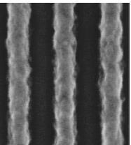
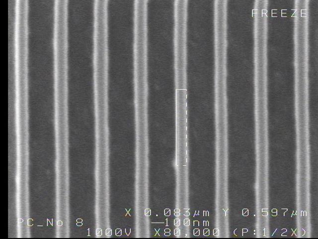
19 Line edge Roughness

20 Simulation of a PE Bake Blocked sites Unreacted polymer Latent Image Edge Gerard Schmid


21 Influence of Base on LER Base quencher can decrease the acid sphere of influence in low contrast regions, thereby reducing LER. I(x) Acid Base x No base With base J. E. Meiring, T. B. Michaelson, G. M. Schmid and C. G. Willson, Proc. SPIE, 5753(2005), to be published
 x x x 0% base 15% base 30% base 6.61 nm RMS 5.47 nm RMS 3.89 nm RMS J. E. Meiring, T. B. Michaelson, G. M. Schmid and C. G. Willson, Proc.")
22 Exploring Base Effects To add base quencher seems to make the contrast higher, thereby LER reducing. I(x) x x x 0% base 15% base 30% base 6.61 nm RMS 5.47 nm RMS 3.89 nm RMS J. E. Meiring, T. B. Michaelson, G. M. Schmid and C. G. Willson, Proc. SPIE, 5753(2005), to be published
23 Typical ArF KrF system always shows dramatic moderate variation of DR dissolution dissolution rate(a/sec) Comparison of ArF and KrF Low contrast value Gradually increasing DR No Unexposed area 0< Unexposed area No DR changes until this point DSE(mJ/cm2) Moderate Rmax Uniform DR inside film Quite high Rmax Different DR inside film Suddenly the dissolution begins The contrast is very high total total surface surface middle middle bottom bottom

24 DR Dissolution behavior KrF System H ArF System This difference in the contrast amplifies small variations in the blend region. Digital n/ff switching phenomenon makes the line edge rough.
25 DR Is there such a thing as too much contrast? The KrF system has lower contrast Small fluctiuations cause small changes in dissolution rate.. The ArF system changes from insoluble to soluble over a very narrow dose range Small fluctuations are amplified and cause huge changes in dissolution rate. Stochastic process noise becomes line edge roughness
26 Could have been Can it be done again at 157nm??? Perhaps.but This time it would have been really hard!!
27 Absorption (mm -1 ) of Common Polymers Transmission %!!! Wavelength (nm) resist resist Polystyrene* 6.20 Polynorbornene* 6.10 PMMA* 5.69 Fluorocarbon* 0.70 * R.R.Kunz,et al., Proc. SPIE 3678, 13 (1999). Vacuum UV 2, H 2 absorbs at this wavelength Even hydrocarbons like butane and polyethylene absorb strongly
28 Fluorination of Norbornane Skeleton F F paque n F F n Transparent? F? 248 nm 193 nm 157 nm How many fluorines and where to fluorinate?
29 Selective Fluorination of Norbornane F Absorbance (mtorr -1 cm -1 ) F F F F F Wavelength (nm) Geminal substitution at the two carbon bridge is the most effective fluorination pattern -CF 3 acrylates
30 Surprising Serendipitous Discovery Ni (II) H + CF 3 CF 3 n n CF 3 CF 3 F 3 C F 3 C H A 157 = 2.57 mm -1 A 157 = 1.15 mm -1 NBHFABC and NBHFA are surprisingly transparent T. Chiba, et. al., J. Photopolym. Sci. Technol, 13 (2000)
31 Absorbance of Fluorinated Polymers CH 3 Absorbance (mm -1 ) (6.02 mm -1 ) CH 2 C CMe (5.42 mm -1 ) CF 3 CH 2 C CMe CF 3 CF 3 (2.68 mm -1 ) (2.44 mm -1 ) Wavelength (nm) CF 3 CF 3 (1.15 mm -1 ) Hexafluoroisopropyl and -trifluoromethylcarboxylic acid are groups surprisingly transparent! H


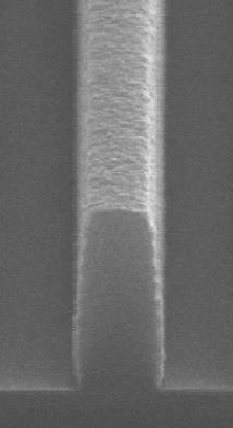
32 Some Imaging Results 100nm 90nm 80nm 60nm 40nm

33 Performance Resist and Process Development Basic Chemistry 60nm Formulation and Process Development 248nm ptimization I-line 157 nm 193nm We are well off the base line Time


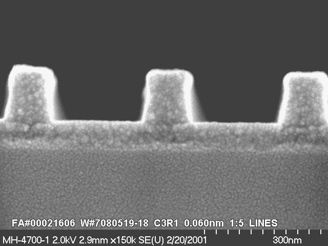
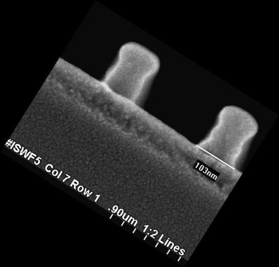

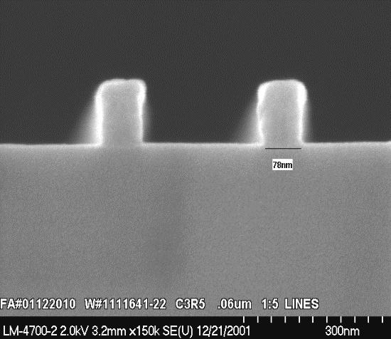


34 Images in UT 157nm Resists 70nm Intel Announcement Issues include: Pace, Resist, Pellicles, CaF 2, Birefringence, Cost, etc. 85nm 60nm 34
EUV Resist-Fundamental Research
 EUV Resist-Fundamental Research Akinori Saeki, Hiroki Yamamoto, Takahiro Kozawa, and Seiichi Tagawa The Institute of Scientific and Industrial Research, Osaka University CREST, Japan Science and Technology
Fundamental aspects of Photosensitized chemically amplified resist (PSCAR) and CAR: How to overcome RLS trade-off and photon shot noise problems
 and CAR: How to overcome RLS trade-off and photon shot noise problems") Fundamental aspects of Photosensitized chemically amplified resist (PSCAR) and CAR: How to overcome RLS trade-off and photon shot noise problems Seiichi Tagawa The Institute of Scientific and Industrial
Fundamental aspects of Photosensitized chemically amplified resist (PSCAR) and CAR: How to overcome RLS trade-off and photon shot noise problems Seiichi Tagawa The Institute of Scientific and Industrial
Functional Materials for Advanced Patterning Robert D. Allen. IBM Almaden Research Center
 Functional Materials for Advanced Patterning Robert D. Allen Business Unit or Product Name IBM Almaden Research Center 2003 IBM Corporation Resists/Materials for Advanced Patterning Trends in Lithography
Particle Generation during Photoresist Dissolution
 Particle Generation during Photoresist Dissolution Siddharth Chauhan a, Mark Somervell b, Michael Carcasi b, Steven Scheer b, Roger T. Bonnecaze a, Chris Mack c and C. Grant Willson a a Department of Chemical
Introduction. Photoresist : Type: Structure:
 Photoresist SEM images of the morphologies of meso structures and nanopatterns on (a) a positively nanopatterned silicon mold, and (b) a negatively nanopatterned silicon mold. Introduction Photoresist
Effect of PAG Location on Resists for Next Generation Lithographies
 Effect of PAG Location on Resists for Next Generation Lithographies ber Research Group Materials Science & Engineering Ithaca, NY 14853 Development Trends in Microlithography 10 Contact Printer Architectures
Relationships between Stochastic Phenomena and Optical Contrast in Chemically Amplified Resist Process of Extreme Ultraviolet Lithography
 Journal of Photopolymer Science and Technology Volume 7, Number () 9 SPST Relationships between Stochastic Phenomena and Optical Contrast in Chemically Amplified Resist Process of Extreme Ultraviolet Lithography
Lithographic Effects Of Acid Diffusion In Chemically Amplified Resists
 INTERFACE '95 This paper was published in the proceedings of the OCG Microlithography Seminar, Interface '95, pp. 217-228. It is made available as an electronic reprint with permission of OCG Microelectronic
Photolithography Overview 9/29/03 Brainerd/photoclass/ECE580/Overvie w/overview
 http://www.intel.com/research/silicon/mooreslaw.htm 1 Moore s law only holds due to photolithography advancements in reducing linewidths 2 All processing to create electric components and circuits rely
Simulation Based Formulation of a Non-Chemically Amplified Resist for 257 nm Laser Mask Fabrication
 Simulation Based Formulation of a Non-Chemically Amplified Resist for 257 nm Laser Mask Fabrication Benjamen M. Rathsack, Cyrus E. Tabery, Timothy B. Stachowiak, Jeff Albelo 2 and C. Grant Willson Department
Sensitization mechanisms of chemically amplified EUV resists and resist design for 22 nm node. Takahiro Kozawa and Seiichi Tagawa
 Sensitization mechanisms of chemically amplified EUV resists and resist design for 22 nm node Takahiro Kozawa and Seiichi Tagawa The Institute of Scientific and Industrial Research, Osaka University, 8-1
Copyright 1997 by the Society of Photo-Optical Instrumentation Engineers.
 Copyright 1997 by the Society of Photo-Optical Instrumentation Engineers. This paper was published in the proceedings of Advances in Resist Technology and Processing XIV, SPIE Vol. 3049, pp. 706-711. It
More on Stochastics and the Phenomenon of Line-Edge Roughness
 More on Stochastics and the Phenomenon of Line-Edge Roughness Chris A. Mack 34 th International Photopolymer Science and Technology Conference Chiba, Japan, June 28, Conclusions We need more than just
Screening of basic resist materials and PAGs for EUV-Lithography
 Screening of basic resist materials and PAGs for EUV-Lithography 1. Int. EUVL-Symposium, Dallas, TX Klaus Lowack, Wolf-Dieter Domke, liver Kirch, Karl Kragler, Heinz-Ulrich Scheunemann* Infineon Technologies
Optimizing RLS. Seiichi Tagawa. The Institute of Scientific and Industrial Research Osaka University and JST-CREST
 Optimizing RLS Seiichi Tagawa The Institute of Scientific and Industrial Research Osaka University and JST-CREST IEUVI Resist TWG October 2, 2008 Acknowledgement Prof. Takahiro Kozawa Dr. Akinori Kozawa
J. Photopolym. Sci. Technol., Vol. 22, No. 5, Fig. 1. Orthogonal solvents to conventional process media.
 originates from the limited number of options regarding orthogonal solvents, i.e. solvents that do not dissolve or adversely damage a pre-deposited organic materials layer. The simplest strategy to achieve
Application of Stochastic Modeling to Resist Optimization Problems
 Application of Stochastic Modeling to Resist Optimization Problems John J. Biafore, Mark D. Smith KLA-Tencor, FINLE Division, North Capital of Texas Highway, Austin, TX 779 BACKGROUND: Modifying specific
Polymer Matrix Effects on EUV Acid Generation
 Polymer Matrix Effects on EUV Acid Generation Theodore H. Fedynyshyn, Russell B. Goodman, and Jeanette Roberts # Lincoln Laboratory Massachusetts Institute of Technology # Intel Corporation The Lincoln
Lecture 8. Photoresists and Non-optical Lithography
 Lecture 8 Photoresists and Non-optical Lithography Reading: Chapters 8 and 9 and notes derived from a HIGHLY recommended book by Chris Mack, Fundamental Principles of Optical Lithography. Any serious student
RLS Trade-Off: Questions about Molecular Size and Quantum Yield
 RLS Trade-Off: Questions about Molecular Size and Quantum Yield Robert Brainard and Craig Higgins Supported by SEMATECH and Rohm and Haas 10/2/08 1 Outline I. Introduction II. III. IV. Effect of Molecular
Single Layer Fluoropolymer Resists for 157 nm Lithography
 Single Layer Fluoropolymer Resists for 157 nm Lithography M. K. Crawford *, W. B. Farnham, A. E. Feiring, J. Feldman, R. H. French, K. W. Leffew, V. A. Petrov, W. Qiu, F. L. Schadt III, H.V. Tran, R. C.
Electron-beam SAFIER process and its application for magnetic thin-film heads
 Electron-beam SAFIER process and its application for magnetic thin-film heads XiaoMin Yang, a) Harold Gentile, Andrew Eckert, and Stanko R. Brankovic Seagate Research Center, 1251 Waterfront Place, Pittsburgh,
Composition and Photochemical Mechanisms of Photoresists
 OpenStax-CNX module: m25525 1 Composition and Photochemical Mechanisms of Photoresists Andrew R. Barron This work is produced by OpenStax-CNX and licensed under the Creative Commons Attribution License
Is an EUV Film Quantum Yield of 30 Possible?
 Is an EUV Film Quantum Yield of 30 Possible? February 21, 2016 Resist TWG San Jose, CA Greg Denbeaux, Amrit Narasimhan, Steven Grzeskowiak, and Robert L. Brainard SUNY Polytechnic Institute Resist TWG
A Simple Model of Line-Edge Roughness
 A Simple Model of Line-Edge Roughness Chris A. Mack www.lithoguru.com Abstract A stochastic modeling approach is used to predict the results of the exposure and post-exposure bake of a chemically amplified
Lecture 14 Advanced Photolithography
 Lecture 14 Advanced Photolithography Chapter 14 Wolf and Tauber 1/74 Announcements Term Paper: You are expected to produce a 4-5 page term paper on a selected topic (from a list). Term paper contributes
Study of Deprotection Reaction during Exposure in Chemically Amplified Resists for Lithography Simulation
 Study of Deprotection Reaction during Exposure in hemically Amplified Resists for Lithography Simulation Yasuhiro Miyake, Mariko Isono and Atsushi Sekiguchi Litho Tech Japan orporation, 2-6-6-201, Namiki,
Development of Lift-off Photoresists with Unique Bottom Profile
 Transactions of The Japan Institute of Electronics Packaging Vol. 8, No. 1, 2015 [Technical Paper] Development of Lift-off Photoresists with Unique Bottom Profile Hirokazu Ito, Kouichi Hasegawa, Tomohiro
Spatial distribution of reaction products in positive tone chemically amplified resists
 Spatial distribution of reaction products in positive tone chemically amplified resists Gerard M. Schmid and Michael D. Stewart Department of Chemical Engineering, The University of Texas at Austin, Austin,
Surface and line-edge roughness in solution and plasma developed negative tone resists: Experiment and simulation
 Surface and line-edge roughness in solution and plasma developed negative tone resists: Experiment and simulation G. P. Patsis, A. Tserepi, I. Raptis, N. Glezos, and E. Gogolides a) Institute of Microelectronics,
EUVL Readiness for High Volume Manufacturing
 EUVL Readiness for High Volume Manufacturing Britt Turkot Intel Corporation Outline Exposure Tool Progress Power Availability Intel demo results Reticle Defectivity Pellicle Materials Conclusion 2 Source
Exploration of non-chemically amplified resists based on chain-scission mechanism for 193 nm lithography
 Rochester Institute of Technology RIT Scholar Works Theses Thesis/Dissertation Collections 2010 Exploration of non-chemically amplified resists based on chain-scission mechanism for 193 nm lithography
Methodology of modeling and simulating line-end shortening effects in deep-uv resist
 Methodology of modeling and simulating line-end shortening effects in deep-uv resist Mosong Cheng*, Ebo Croffie, Andrew Neureuther Electronics Research Laboratory Department of Electrical Engineering and
Application of polymers to photoresist materials
 Nippon Gomu Kyokaishi, No. 2, 2012, pp. 33 39 Application of polymers to photoresist materials A. Soyano Semiconductor Materials Laboratory, Fine Electronics Materials Research Laboratories, JSR Corporation,
Surface roughness development during photoresist dissolution
 Surface roughness development during photoresist dissolution Lewis W. Flanagin, a) Vivek K. Singh, b) and C. Grant Willson c) Department of Chemical Engineering, The University of Texas at Austin, Austin,
5. Photochemistry of polymers
 5. Photochemistry of polymers 5.1 Photopolymerization and cross-linking Photopolymerization The fundamental principle of photopolymerization is based on the photoinduced production of a reactive species,
Lithography Challenges Moore s Law Rising Costs and Challenges of Advanced Patterning
 Lithography Challenges Moore s Law Rising Costs and Challenges of Advanced Patterning SEMI Texas Spring Forum May 21, 2013 Austin, Texas Author / Company / Division / Rev. / Date A smartphone today has
DUV Positive Photoresists
 Journal of Photopolymer Science and Technology Volume 5, Number 1(1992) 207-216 Factors Affecting the Performance of Chemically DUV Positive Photoresists Amplified James W. Thackeray, Theodore H. Fedynyshyn,
Seiichi Tagawa, Satoshi Enomoto, Akihiro Oshima
 Time Resolved Spectroscopy of Nanoparticle EUV Photoresists Reactions of HfO nanoparticles with electrons and the following solubility change studied by pulse radiolysis Seiichi Tagawa, Satoshi Enomoto,
Radiation Chemistry of EUV and EB Resists
 Radiation Chemistry of EUV and EB Resists Tagawa 1,2,3 1 The Institute of Scientific and Industrial Research, Osaka University, 2 Japan Science and Technology Agency, CREST, c/o Osaka University, 8-1 Mihogaoka,
Photoresist etch resistance enhancement using novel polycarbocyclic derivatives as additives
 Photoresist etch resistance enhancement using novel polycarbocyclic derivatives as additives Evangelos Gogolides and Panagiotis Argitis Institute of Microelectronics, NCSR Demokritos, Aghia Paraskevi 15310,
Development of Photosensitive Polyimides for LCD with High Aperture Ratio. May 24, 2004
 Development of Photosensitive Polyimides for LCD with High Aperture Ratio May 24, 2004 utline Why is polymer dielectric required for TFT LCD? Requirements of the polymer dielectrics What is polyimide?
Line-Edge Roughness and the Impact of Stochastic Processes on Lithography Scaling for Moore s Law
 Line-Edge Roughness and the Impact of Stochastic Processes on Lithography Scaling for Moore s Law Chris A. Mack Lithoguru.com, 1605 Watchhill Rd, Austin, TX 78703 Abstract Moore s Law, the idea that every
Molecular Glass Resist with Organic Developer
 1 Molecular Glass Resist with Organic Developer James M. Blackwell 1,2 Armando Ramirez 1 Hiroki Nakagawa 1,3 Yoshi Hishiro 3 1 Intel's Molecules for Advanced Patterning(MAP) Program, LBNL Molecular Foundry,
NanoImprint Materials. March, IBM Almaden Research Center
 NanoImprint Materials Ratnam Sooriyakumaran Hiroshi Ito Mark Hart Frances Houle Geraud Dubois Robert Miller Robert Allen March, 2006 05/24/2006 Imprint in IBM IBM Research Division is conducting an exploratory
DIFFUSION OF ACID AND ACTIVATION ENERGY OF POSITIVE CHEMICAL AMPLIFICATION RESIST
 Journal of Photopolymer Science and Technology Volume 6, Number 4(1993) 505-514 1993TAPJ DIFFUSION OF ACID AND ACTIVATION ENERGY OF POSITIVE CHEMICAL AMPLIFICATION RESIST Koi 7ASAKAWA Toshiba Research
Line Edge Roughness, part 2
 Tutor57D.doc: Version 3/19/07 Line Edge Roughness, part T h e L i t h o g r a p h y E x p e r t (ay 007) In the last edition of this column [1], I began the difficult process of trying to understand the
Effects of photoresist polymer molecular weight on line-edge roughness and its metrology probed with Monte Carlo simulations
 Microelectronic Engineering xxx (2004) xxx xxx www.elsevier.com/locate/mee Effects of photoresist polymer molecular weight on line-edge roughness and its metrology probed with Monte Carlo simulations G.P.
Top down and bottom up fabrication
 Lecture 24 Top down and bottom up fabrication Lithography ( lithos stone / graphein to write) City of words lithograph h (Vito Acconci, 1999) 1930 s lithography press Photolithography d 2( NA) NA=numerical
Title. CitationChemical physics letters, 657: Issue Date Doc URL. Rights
 Title Dynamics of radical cations of poly(4-hydroxystyrene determined by pulse radiolysis of its highly concent Author(s)Okamoto, Kazumasa; Ishida, Takuya; Yamamoto, Hiroki; CitationChemical physics letters,
EFFECT OF NANOSCALE CONFINEMENT ON THE PHYSICAL PROPERTIES OF POLYMER THIN FILMS
 EFFECT OF NANOSCALE CONFINEMENT ON THE PHYSICAL PROPERTIES OF POLYMER THIN FILMS A Thesis Presented to The Academic Faculty by Lovejeet Singh In Partial Fulfillment of the Requirements for the Degree Doctor
Simulation and characterization of surface and line edge roughness in photoresists before and after etching
 Simulation and characterization of surface and line edge roughness in photoresists before and after etching Motivation of this work : Sub 100nm lithographic features often suffer from roughness. Need to
A Physically Based Model for Predicting Volume Shrinkage in Chemically Amplified Resists
 A Physically Based Model for Predicting Volume Shrinkage in Chemically Amplified Resists Nickhil Jakatdar 1, Junwei Bao, Costas J. Spanos Dept. of Electrical Engineering and Computer Sciences, University
EUV Reflectometry for Determining the Optical Properties of Photoresists and Underlayer Materials Upon Irradiation at 13.5-nm
 EUV Reflectometry for Determining the Optical Properties of Photoresists and Underlayer Materials Upon Irradiation at 13.5-nm Grace H. Ho, 1 Fu-H. Kang, 1 Yu-H. Shih, 1 Hok-S. Fung, Hwang-W. Fu, Rikimaru
Hiroshi Ito and Mark Sherwood. IBMAlmaden Research Center 650 Harry Road San Jose, CA 95120, U S. A ibm. com.
 Journal of Photopolymer Science and Technology Volumel2,Number4(1999) 625-636 1999TAPJ Investigation of Deep UV Solvents, Chemistries, Resists by NMR: Residual and PAG Decomposition in Casting Film Hiroshi
The deprotection reaction front profile in model 193 nm methacrylate-based chemically amplified photoresists
 The deprotection reaction front profile in model 193 nm methacrylate-based chemically amplified photoresists Bryan D. Vogt a, Shuhui Kang a, Vivek M. Prabhu *a, Ashwin Rao a, Eric K. Lin a, Sushil K. Satija
The Journal of American Science, 4(1), 2008, ISSN ,
, 2008, ISSN ,") Free adical-induced Copolymerization of Norbornene and Methacrylate An-chi Yeh Department of Chemical and Material Engineering Chengshiu University, Niaosong, Kaohsiung, Taiwan, 833 C E-mail: acyeh1965@yahoo.com.tw
Free adical-induced Copolymerization of Norbornene and Methacrylate An-chi Yeh Department of Chemical and Material Engineering Chengshiu University, Niaosong, Kaohsiung, Taiwan, 833 C E-mail: acyeh1965@yahoo.com.tw
Developer-soluble Gap fill materials for patterning metal trenches in Via-first Dual Damascene process
 Developer-soluble Gap fill materials for patterning metal trenches in Via-first Dual Damascene process Mandar Bhave, Kevin Edwards, Carlton Washburn Brewer Science, Inc., 2401 Brewer Dr., Rolla, MO 65401,
Exploration of non-chemically amplified resists based on dissolution inhibitors for 193 nm lithography
 Rochester Institute of Technology RIT Scholar Works Theses Thesis/Dissertation Collections 2010 Exploration of non-chemically amplified resists based on dissolution inhibitors for 193 nm lithography Burak
Lawrence Berkeley National Laboratory Lawrence Berkeley National Laboratory
 Lawrence Berkeley National Laboratory Lawrence Berkeley National Laboratory Title Spatial scaling metrics of mask-induced induced line-edge roughness Permalink https://escholarship.org/uc/item/5rc666c3
Lithography and Etching
 Lithography and Etching Victor Ovchinnikov Chapters 8.1, 8.4, 9, 11 Previous lecture Microdevices Main processes: Thin film deposition Patterning (lithography) Doping Materials: Single crystal (monocrystal)
Acid Quantum Efficiency of Anion-bound Chemically Amplified Resists upon Exposure to Extreme Ultraviolet Radiation
 Journal of Photopolymer Science and Technology Volume 28, Number 4 (2015) 501 505 2015SPST Acid Quantum Efficiency of Anion-bound Chemically Amplified Resists upon Exposure to Extreme Ultraviolet Radiation
Swing Curves. T h e L i t h o g r a p h y T u t o r (Summer 1994) Chris A. Mack, FINLE Technologies, Austin, Texas
 Chris A. Mack, FINLE Technologies, Austin, Texas") T h e L i t h o g r a p h y T u t o r (Summer 1994) Swing Curves Chris A. Mack, FINLE Technologies, Austin, Texas In the last edition of this column, we saw that exposing a photoresist involves the propagation
T h e L i t h o g r a p h y T u t o r (Summer 1994) Swing Curves Chris A. Mack, FINLE Technologies, Austin, Texas In the last edition of this column, we saw that exposing a photoresist involves the propagation
Fabrication of Sub-Quarter-Micron Grating Patterns by Employing Lithography
 MCROU,!~'O~C ELSEVER Microelectronic Engineering 46 (1999) 173-177 Fabrication of Sub-Quarter-Micron Grating Patterns by Employing Lithography DUV Holographic L. A. Wang*, C. H. Lin and J. H. Chen nstitute
Orthogonal Processing: A New Strategy for Patterning Organic Electronics
 1 rthogonal Processing: A New Strategy for Patterning rganic Electronics ERC Teleconference 3/September/2009 Jin-Kyun Lee and Christopher K. ber* Materials Science & Engineering Cornell University 2 rganic
Stochastic modeling of photoresist development in two and three dimensions
 J. Micro/Nanolith. MEMS MOEMS 9(4), 04202 (Oct Dec 200) Stochastic modeling of photoresist development in two and three dimensions Chris A. Mack 605 Watchhill Road Austin, Texas 78703 E-mail: chris@lithoguru.com
A Study of the Fundamental Contributions to Line Edge Roughness in a 193 nm, Top Surface Imaging System
 A Study of the Fundamental Contributions to Line Edge Roughness in a 193 nm, Top Surface Imaging System Mark H. Somervell Department of Chemical Engineering, The University of Texas at Austin, Austin,
Recent progress in nanoparticle photoresist development for EUV lithography
 Recent progress in nanoparticle photoresist development for EUV lithography Kazuki Kasahara ab, Vasiliki Kosma b, Jeremy Odent b, Hong Xu b, Mufei Yu b, Emmanuel P. Giannelis b, Christopher K. Ober b a
Photolithography II ( Part 1 )
") 1 Photolithography II ( Part 1 ) Chapter 14 : Semiconductor Manufacturing Technology by M. Quirk & J. Serda Bjørn-Ove Fimland, Department of Electronics and Telecommunication, Norwegian University of Science
1 Photolithography II ( Part 1 ) Chapter 14 : Semiconductor Manufacturing Technology by M. Quirk & J. Serda Bjørn-Ove Fimland, Department of Electronics and Telecommunication, Norwegian University of Science
A Study of Resolution Limits Due to Intrinsic Bias in Chemically Amplified Photoresists.
 A Study of Resolution Limits Due to Intrinsic Bias in Chemically Amplified Photoresists. Sergei V. Postnikov, Michael D. Stewart, Hoang Vi Tran, Mark A. Nierode, David R. Medeiros, T. Cao, Jeffrey Byers,
Current Status of Inorganic Nanoparticle Photoresists
 Prof. Christopher K. ber Department of Materials Science and Engineering, Cornell University, Ithaca NY Current Status of Inorganic Nanoparticle Photoresists Markos Trikeriotis, Marie Krysak, Yeon Sook
Molecular Organometallic Resists for EUV (MORE) October 6, 2013
 October 6, 2013") Molecular Organometallic Resists for EUV (MORE) October 6, 2013 Brian Cardineau, 1 James Passarelli, 1 Miriam Sortland, 1 Ryan Del Re, 1 Westly Tear, 1 Hashim Al-Mashat, 2 Miles Marnell, 2 Kara Heard,
Molecular Organometallic Resists for EUV (MORE) October 6, 2013 Brian Cardineau, 1 James Passarelli, 1 Miriam Sortland, 1 Ryan Del Re, 1 Westly Tear, 1 Hashim Al-Mashat, 2 Miles Marnell, 2 Kara Heard,
Chapter 5. Ionic Polymerization. Anionic.
 Chapter 5. Ionic Polymerization. Anionic. Anionic Polymerization Dr. Houston S. Brown Lecturer of Chemistry UH-Downtown brownhs@uhd.edu What you should know: What is anionic polymerization? What is MWD,
Photoinitiation, Photopolymerization, and Photocuring
 Jean-Pierre Fouassier Photoinitiation, Photopolymerization, and Photocuring Fundamentals and Applications Hanser Publishers, Munich Vienna New York Hanser/Gardner Publications, Inc., Cincinnati Contents
Takeo Watanabe Center for EUVL, University of Hyogo
 Soft X-ray Absorption Spectroscopy using SR for EUV Resist Chemical Reaction Analysis Takeo Watanabe Center for EUVL, University of Hyogo Outline 1) Background 2) Princple of X-ray absorption spectroscopy
Behavior of candidate organic pellicle materials under 157 nm laser irradiation
 Behavior of candidate organic pellicle materials under 157 nm laser irradiation A. Grenville Intel / International SEMATECH Austin, TX 78741-6499 V. Liberman, M. Rothschild, J.H.C. Sedlacek Lincoln Laboratory,
Photonics applications 5: photoresists
 IMI-NFG s Mini Course on Chalcogenide Glasses Lecture 11 Photonics applications 5: photoresists Himanshu Jain Department of Materials Science & Engineering Lehigh University, Bethlehem, PA 18015 H.Jain@Lehigh.edu
Chapter 2 Process Variability. Overview. 2.1 Sources and Types of Variations
 Chapter 2 Process Variability Overview Parameter variability has always been an issue in integrated circuits. However, comparing with the size of devices, it is relatively increasing with technology evolution,
UNIT 3. By: Ajay Kumar Gautam Asst. Prof. Dev Bhoomi Institute of Technology & Engineering, Dehradun
 UNIT 3 By: Ajay Kumar Gautam Asst. Prof. Dev Bhoomi Institute of Technology & Engineering, Dehradun 1 Syllabus Lithography: photolithography and pattern transfer, Optical and non optical lithography, electron,
Overview of the main nano-lithography techniques
 Overview of the main nano-lithography techniques Soraya Sangiao sangiao@unizar.es Outline Introduction: Nanotechnology. Nano-lithography techniques: Masked lithography techniques: Photolithography. X-ray
Copyright 1999 by the Society of Photo-Optical Instrumentation Engineers.
 Copyright 1999 by the Society of Photo-Optical Instrumentation Engineers. This paper was published in the proceedings of Advances in Resist Technology and Processing XVI, SPIE Vol. 3678, pp. 1-1011. It
Silicon VLSI Technology. Fundamentals, Practice and Modeling
 Text Book: Silicon VLSI Technology Fundamentals, Practice and Modeling Authors: J. D. Plummer, M. D. Deal, and P. B. Griffin Photolithography (Chap. 1) Basic lithography process Apply photoresist Patterned
Photolithography 光刻 Part II: Photoresists
 微纳光电子材料与器件工艺原理 Photolithography 光刻 Part II: Photoresists Xing Sheng 盛兴 Department of Electronic Engineering Tsinghua University xingsheng@tsinghua.edu.cn 1 Photolithography 光刻胶 负胶 正胶 4 Photolithography
Understanding Molecular Level Effects during Post Exposure Processing
 Understanding Molecular Level Effects during Post Exposure Processing Gerard M. Schmid *a, Mark D. Smith b, Chris A. Mack b, Vivek K. Singh c, Sean D. Burns a, and C. Grant Willson a a The University of
Copyright 1999 by the Society of Photo-Optical Instrumentation Engineers.
 Copyright 1999 by the Society of Photo-Optical Instrumentation Engineers. This paper was published in the proceedings of Lithography for Semiconductor Manufacturing SPIE Vol. 3741, pp. 148-160. It is made
Supporting Information
 Electronic Supplementary Material (ESI) for ChemComm. This journal is The Royal Society of Chemistry 2014 Supporting Information Synthesis of Poly(dihydroxystyrene-block-styrene) (PDHSt-b-PSt) by the RAFT
Direct write electron beam patterning of DNA complex thin films
 Direct write electron beam patterning of DNA complex thin films R. A. Jones, W. X. Li, H. Spaeth, and A. J. Steckl a Nanoelectronics Laboratory, University of Cincinnati, Cincinnati, Ohio 45221-0030 Received
Supporting Information. for. Angew. Chem. Int. Ed. Z Wiley-VCH 2004
 Supporting Information for Angew. Chem. Int. Ed. Z53009 Wiley-VCH 2004 69451 Weinheim, Germany Shear Patterning of Microdominos: A New Class of Procedures for Making Micro- and Nanostructures ** Byron
Secondaryionmassspectrometry
 Secondaryionmassspectrometry (SIMS) 1 Incident Ion Techniques for Surface Composition Analysis Mass spectrometric technique 1. Ionization -Electron ionization (EI) -Chemical ionization (CI) -Field ionization
MICRO AND NANOPROCESSING TECHNOLOGIES
 LECTURE 5 MICRO AND NANOPROCESSING TECHNOLOGIES Introduction Ion lithography X-ray lithography Soft lithography E-beam lithography Concepts and processes Lithography systems Masks and resists Chapt.9.
EE C245 ME C218 Introduction to MEMS Design Fall 2007
 EE C245 ME C218 Introduction to MEMS Design Fall 2007 Prof. Clark T.-C. Nguyen Dept. of Electrical Engineering & Computer Sciences University of California at Berkeley Berkeley, CA 94720 Lecture 5: ALD,
Advances in 2D and 3D Patterning for Nanotechnology
 Advances in 2D and 3D Patterning for Nanotechnology Christopher K. ber, Young Cheol Bae 1, Tianyue Yu, Mingqi Li and Katsuji Douki 2 Cornell University, Materials Science & Engineering, 310 Bard Hall,
A Parameter Extraction Framework for DUV Lithography Simulation
 A Parameter Extraction Framework for DUV Lithography Simulation Nickhil Jakatdar 1, Junwei Bao, Costas J. Spanos Dept. of Electrical Engineering and Computer Sciences, University of California at Berkeley,
Surface and Interface Characterization of Polymer Films
 Surface and Interface Characterization of Polymer Films Jeff Shallenberger, Evans Analytical Group 104 Windsor Center Dr., East Windsor NJ Copyright 2013 Evans Analytical Group Outline Introduction to
Chapter 3 : ULSI Manufacturing Technology - (c) Photolithography
 Photolithography") Chapter 3 : ULSI Manufacturing Technology - (c) Photolithography 1 Reference 1. Semiconductor Manufacturing Technology : Michael Quirk and Julian Serda (2001) 2. - (2004) 3. Semiconductor Physics and Devices-
Chapter 3 : ULSI Manufacturing Technology - (c) Photolithography 1 Reference 1. Semiconductor Manufacturing Technology : Michael Quirk and Julian Serda (2001) 2. - (2004) 3. Semiconductor Physics and Devices-
Improving resist resolution and sensitivity via electric-field enhanced postexposure baking
 Improving resist resolution and sensitivity via electric-field enhanced postexposure baking Mosong Cheng, a) Lei Yuan, Ebo Croffie, and Andrew Neureuther Electronics Research Laboratory, University of
Enhanced Transmission by Periodic Hole. Arrays in Metal Films
 Enhanced Transmission by Periodic Hole Arrays in Metal Films K. Milliman University of Florida July 30, 2008 Abstract Three different square periodic hole arrays were manufactured on a silver film in order
DUV ( nm ) Characterization of Materials: A new instrument, the Purged UV Spectroscopic Ellipsometer,
 Characterization of Materials: A new instrument, the Purged UV Spectroscopic Ellipsometer,") WISE 2000, International Workshop on Spectroscopic Ellipsometry, 8 9 May 2000 DUV (150 350nm ) Characterization of Materials: A new instrument, the Purged UV Spectroscopic Ellipsometer, Pierre BOHER,,
WISE 2000, International Workshop on Spectroscopic Ellipsometry, 8 9 May 2000 DUV (150 350nm ) Characterization of Materials: A new instrument, the Purged UV Spectroscopic Ellipsometer, Pierre BOHER,,
Novel Molecular Materials Based on Noria and Double Calixarene (Beryllus) for EB and EUV Resist Systems
 for EB and EUV Resist Systems") 2010 International Workshop on EUV Lithography Makena Beach Golf Resort June 21-25, 25, 2010, Maui, Hawaii Novel Molecular Materials Based on Noria and Double Calixarene (Beryllus) for EB and EUV Resist
2010 International Workshop on EUV Lithography Makena Beach Golf Resort June 21-25, 25, 2010, Maui, Hawaii Novel Molecular Materials Based on Noria and Double Calixarene (Beryllus) for EB and EUV Resist
TRANSPARENT LAYERS OF AZO CONJUGATED POLYMERS: PREPARATION AND OPTO ELECTRICAL PROPERTIES
 Journal of Optoelectronics and Advanced Materials Vol., No.,, p. - Section : Organic materials TRANSPARENT LAYERS OF AZO CONJUGATED POLYMERS: PREPARATION AND OPTO ELECTRICAL PROPERTIES "Petru Poni" Institute