Nanofabrication Techniques. Dominique Mailly Laboratoire de Photonique et de Nanostructures Marcoussis
|
|
|
- Jemima Lane
- 6 years ago
- Views:
Transcription
1 Nanofabrication Techniques Dominique Mailly Laboratoire de Photonique et de Nanostructures Marcoussis
2 Summary Introduction Optical Lithography X-ray lithography E-beam Lithography Ion beam Lithography Near field Lithography Soft and Imprint Lithography Transfert techniques
3 Typical Flowchart for fabrication substrat Resist spinning exposure development Metal deposition lift-off etching Electrolytic growth
4 lithography Crucial step which will fix the size of the pattern Lentille g contact 1:1 projection 1:5 à 1:20 Focused beam writing
5 Moore Law
6 Resist and contrast Contrairely to photography one does not want any gray scale The highest contrast is the best. negative resist positive resist
7 Optical lithography by contact or proximity gap b b b e Light intensity on resist mask resist wafer Ideal transfert Real transfert resolution limited by diffraction: t= λg gap minimum=resist thickness Substrats flatness Resist damage Mask damage mask1:1 e.g. g=10µm, l=400nm t=10µm Typically in a lab one can achieve 0.5µm and reach 0.2µm with conformal masks λ >200nm for mask transparency Simple and economical this is the popular lithographic tool for labs and R&D for intermediate resolution
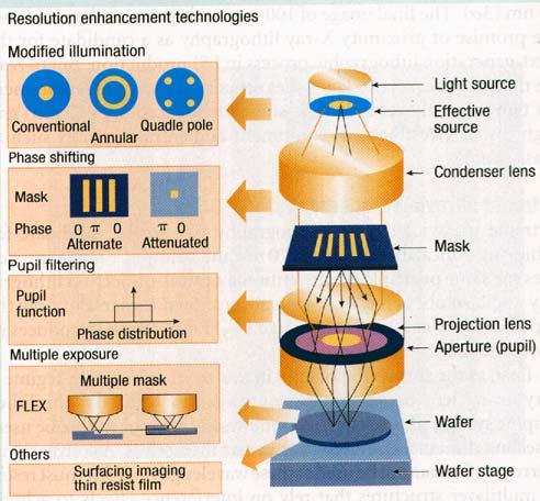
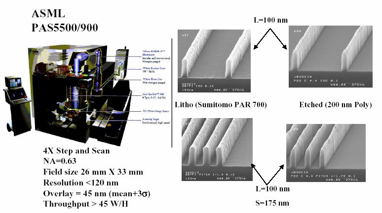
8 Projection Lithography UV light Resolution limited by diffraction: R = k λ N.A. N.A. numerical aperture k technological parameter theoretical k=0.61 (Rayleigh criteria) process parameter lens aperture DOF N.A. -2 NA=n sini i 1:5 to 1:20
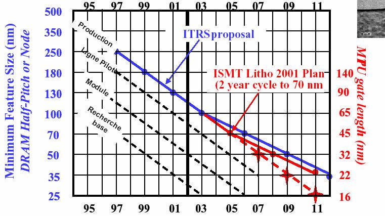
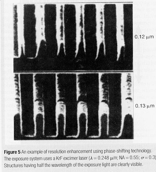
9 Evolution of projection lithography Year λ N.A. resolution k nm µm nm µm nm µm O nm µm nm µm 0.49 k<k Rayleigh top imaging technique and phase shift mask


10 Top imaging technique and phase shift mask k :
11
12 10M! 193nm lithography
13 Refractive mask Reflection mask

14 EUV Lithography EUV are absorbed by all material and gases: need to be in vacuum
15 At the moment the situation is not clear between 157nm/immersion lens and EUV
16 X-ray lithography X photon Choice of wave length: diffraction t=(λg) 1/2 mean free path of photo-electron:l λ α mask transparency absorber efficiency Photo-electron extension 0.8nm < λ < 1.6nm Not sensitive to dust particles large process lattitude diverging source enlargment and shadow Parallel source synchrotron light
17 X-ray mask no X ray optics mask 1:1 absorber:au, W, Ta 0.4µm membrane: Si 3 N 4, SiC 2µm Stand Si Need to control stress of membrane for flatness No stress in absorber Good mechanical stability The major difficulty of X-ray lithography


18 Example of X-ray lithography 30 nm lines onpmma 20 nm dots on PMMA X-ray lithography versus EUV lithography??????


19 3D X-ray lithography Multiple exposures with 3 different angles Photonic crystal
20 Electron beam lithography Since a long time one knows how to focus electrons beam spot < 10nm Very small wavelength: no diffraction limitation Direct writing: maskless sequential writing: small throughput resolution : depends on resist, one can reproduce the spot size i.e. 1nm
21 electron-resist interaction organic resist (PMMA) m m m m m m m m m m m m m m m m non soluble soluble Typical energy for breaking a bond: 10eV Typical energy of the beam : several 10keV (Problem of aberration at low energy)

22 Monte Carlo Simulation to study energy lost Forward scattering Substrat backscattering Spreading of the beam, lost of resolution Energy far from the impact of the beam, proximity effects
23 E(r) β a Double Gaussian model E( r) = aexp + exp r b r βa βb 2 2 β r r Tension kv β a (µm) β r (µm) β a forward scattering: Essentially depends on the resist and the voltage β r backscattering: Depends on the voltage and the substrat Substrat Si
24 How to beat proximity effect Vary the dose depending on the pattern Use high energy: dilute proximity effect on a large area Use very small energy (STM) (but forward scattering) Use resist sensitive to high energy: inorganic resists Write on membranes
25 Proximity effects Dose depends on the pattern Intra proximity Dose depends on the surrounding of the pattern D=E(1+b) Real dose as exposed dose proximity effect
26 Software for proximity effect correction Commercial software exist (very expensive) Correction may needs negative doses at some points! It is very difficult to produce arrays of line with a very fine pitch


27 200kV e-beam lithography on PMMA Line <10nm Granular gold lift-off
28 Multilayer techniques resolution resist layer stoplayer absorber resist (low Z) Substrat (high Z)
29 Resolution of organic Resists
30 Inorganic resist sensitive to high energy Diffusion pump oil Polymerisation under the beam Size few nm (hard to remove!) Other inorganic resist: Al 2 O 3, NaCl, AlF 3, problems: very thin resist :no lift-off very high doses C/cm 2 i.e s/µm!

31 AlF 3 at 200kV
32 The e-beam writer (example of the LEICA 5000)

33 Schottky Emitter Tip <100> W Crystal ZrO Reservoir Polycrystalline tungsten heating filament Brightness >>LaB6 cathode Spot size<5nm at 500pA
34 Scanning Techniques for E-Beam Lithography Beam Scan Area Beam Scan Area Stage Movement Limits 1. Raster Scan The beam deflection system scans a fixed sized area whilst the beam is switched on and off to expose the local areas where shapes are required. 2. Vectorscan The blanked beam is deflected to the lower-left hand corner of a shape. The beam is unblanked and the required shape area then scanned. The beam is again blanked and deflected to the next required shape. 3. Stage Scan/ Static Beam The stage is moved in the path required to create the lithographic shapes while the beam remains undeflected Shaped beam for mask making machine
35 Vector Scan of Rectangle Shape Stop scan and blank beam Un-blank beam and start scan here Beam Step Size
36 Exposure Scan Strategy Main field double-lever scan coils deflect beam to start position of each shape. Final lens Main field
37 Exposure Scan Strategy The Trapezium Deflector scans the required lithography shape at the position within the Main Field set by the Mainfield deflector coils. Final lens Main field Trapezium shape maximum size (depends on EHT)
38 Trapezium Field The main reason for the Trapezium deflection system is speed. It is not possible to deflect the main beam with 25Mhz stepping frequency. Large current changes in inductive deflection coils require long settling times To achieve very fast deflection Use a coil with low self-inductance Limit the range of deflection currents Disadvantages: The deflection range is limited (12.8µm max but depends on EHT). Large shapes require fracturing into Trap deflection range sizes. Advantages: High speed deflection possible Exposure lost time for settling greatly reduced
39 Writing Strategy + Y Field Boundary Block Boundary Substrate on the Holder, on the Stage Trapezia - Positioned by main deflection - Written by Trapezia Scan 0,0 Fields/Blocks positioned by stage movement + X Field Size Shape positioning Resolution = Beam Step Size interval defines Trapezia size
40 Deflection Coils Basic Deflection System Main X Pattern Main Y Computer Generator Clock Trapezium Generator Trap X Trap Y Determine the dose Beam Blanking Beam Blanke r
41 Effects of deflection on the Beam Final Aperture Focal Plain Substrate Surface the pattern has to be divided into field
42 Laser Interferometer Optics Beam Bender 50% Beam Splitter Y Axis Remote Interferometer Laser Optics Box Y Axis Receiver Y Axis Mirror Stage X Axis Laser X Axis Mirror Stage Stage Y Axis Main Chamber Airlock Beam Bender X Axis Receiver X Axis Remote Interferometer The Laser emits a second beam for each axis which is polarized at 90 0 to the first. This beam travels through a different path as shown. It is reflected back to the Receiver by the Remote Interferometer optics and does not see the Stage. This beam measures any changes of path length between the Laser and the Remote Interferometer units. The measurements of the two beams are combined and the resultant signal output provides an accurate measurement of the position of the stage relative to the remote interferometer units. Hence changes of room temperature affecting the path length in the Laser Optics Box do not affect the accuracy of the measurement of the Stage position. Accuracy about 2nm
43 Elements of Beam Error Feedback (Pull-in) R Required Stage Position M Mechanical Stage Position R- M BEF Stage Position Values DAC Laser Interferometer Calibration Scale and Rotation Stage Mirrors Amplifier (R - M) E-Beam Deflection Coils Stage Mechanical Stage position Required Destination
44 e-beam lithography: Highest resolution Low process - not for industrial purpose (for all processes) Intermediate cost : 150k for SEM based equipment 3M for e-beam writer
45 Ion beam lithography Revival of ions beam spot size < 10nm Ions are rapidely absorbed no proximity effect Small doses Tridimensionnal structures Direct writing (without resist) through etching or implantation.
46 Ion trajectories


47 30kV Gallium ions Holes in a Si 3 N 4 membrane 10 nm LPN Marcoussis


48 Ion beam lithography on AlF3 resist 30kV Ga ion

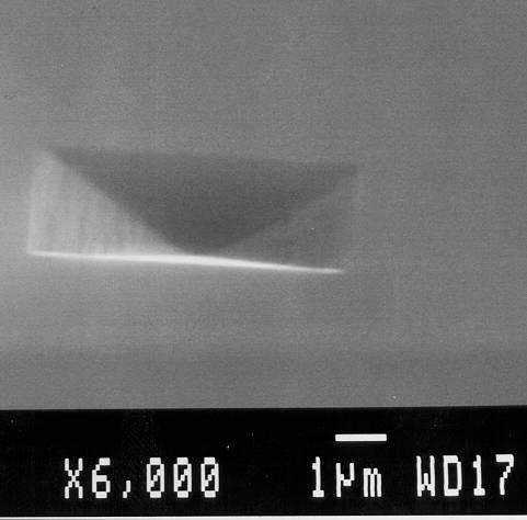
49 3D lithography on organo-metallic gold composite Résist:Au 55 (PPh3) 12 Cl 6 Dimensions : 30 nm wide, 20 nm height : 1.5 µm long. (Ga ions, energy 30 kev, initial thickness 50nm)

 Transparent alumina substrate")

.")
50 Local FIB induced mixing - Thin magnetic films patterning FIB probe Pattern Pt (3,4 nm) Co (1,4 nm) Pt (4,5 nm) Transparent alumina substrate Magneto-optical image of magnetic domains defined between irradiated lines (Ga + ions, 30 kev, ions/cm 2 ). Arrays of stable magnetic dots 1500 nm, 750 nm, 300 nm, 50 nm
51 Tridimensional etching
52 Near field lithography
53 Near field lithography through local electrochemistry example of gold a) Surface water condensation b) Monolayer of oxydize gold H 2 O Gold surface oxygen atoms gold atoms c) Exchange process d) Dissolution of gold atoms
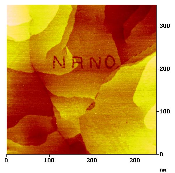
54 examples
55 Near field scheme Electrical pulse Mechanical pressure Below threshold threshold Observation/alignment
56 Local CVD deposition PF 3 PF 3 Rh Cl Cl Rh PF 3 PF 3 depassivation deposit low pressure one pulse one atome 100nm GPEC Marseille


57 Example of useful structures Anodization of GaAs Anodization of Nb ETH Zürich CRTBT

58 Use carbon nanotube to improve the resolution Pb vibrations needs short tube 0.2µm LEPES Grenoble

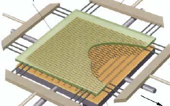
59 Slow process parallel set-up
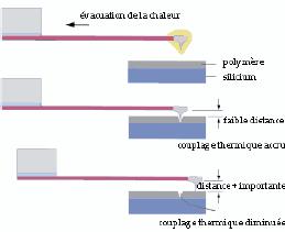
60 Thermal lithography Milliped project IBM Zürich


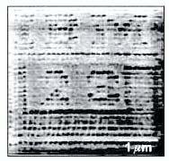
61 Dip pen lithography Application to DNA Chip resolution =40nm Northwestern Univ

62 Nano-imprint 1.temp +pressure 50Bars resist mold substrate 2. cooling 3. Remove mold (tricky!) 4. Etch of residual resist Slow process, Need mask at 1/1 scale i.e. e-beam lithography Resolution demonstrated down to 10nm. Very chip!
63 examples
64 UV assisted imprint Quartz mold substrate UV hardening of the resist Much faster, still problem for alignment, commercial systems now

65 Nano-stamp Use of molecular adhesion Example : thiol group on gold PDMS ink etch thiols Gold Si P = 400 nm
66 Conclusion on lithography techniques Technique Resolution Use Remarks contact 0.25µm Labs and R&D Economical Optical lithography proximity 2µm Labs and R&D projection 80nm Industrial Economical but weak resolution Expensive but with constant progress EUV <50nm Industrial May be the next tehnique for 2005 Electron lithography 1nm Labs andr&d Fabrication of optical masks Technique without mask best resolution Lithographie ionique 8nm Labs and R&D Better for etchig than lithography (diagnostic) Near field lithography Atom 10nm Labs Economical, very slow specific Nanoimprint 10nm Labs and industry? Economical, fast Alignment problems mask 1 :1
67 Transfert techniques Wet etching Ion Beam Etching Reactive Ion Etching Reactive Ion Beam Etching Dense plasma
 too fast Weak etching slow but too sensitive to")
68 isotrope wet etching Simple Fast Do not respect the design rule Wet etching You may think to use under etching to reduce thee size. Difficult to control because of surface state: strong etching (not sensitive to surface state) too fast Weak etching slow but too sensitive to surface state
69 Anisotropic wet etching Use anisotropic etch rate with crystal face Still some under-etch Use to produce nice features over-growth in V-groves Can be mixted with stop layer
70 Ion Beam Etching IBE gas Use the impact of impining ions. Purely physical Sputtering rate T accelerated ions T ZU E U binding energy of material Z atomic number of mateerial E ion energy x coeff (angle)
71 Quite slow No selectivity Re-deposition Trenching damage
72 Reactive ion etching: RIE rf plasma C Autopolarisation few100v Chemically active ions
73 passivation gas Anisotropy achievement

74 Avantages of RIE Fast proceess Selectivity Anisotropy No redeposition Use of passivation layer problems of RIE Sensitive to pollution Energy and pressure are linked


75 Reactive Ion Beam Ething:RIBE Same as IBE but with chemically active ions Allows to separate the physical/chemical action Impressive aspect ratio


76 Examples RIE 1,94µmby 6,25µm AlAs/GaAs miropillar 7.5 µm Depth limited to 1.2mm For 0.4mm diameter holes

77 Example RIBE

")

78 Electron Cyclotron Resonance and Inductive Coupled Plasma High density plasma (fast) with low energy (damage) Independant control of energy/density
79 Top down and bottom up? Both techniques tend to the same dimension Future of nanotechnology will be certainly a mixing of these techniques Addressing of individual macromolecules Structuration of substrat
")
80 Carbone nanotube and e-beam lithography T=30 mk Magnetic field (Gauss) LPN-Marcoussis

81 CVD growth of Carbone Nanotube on structured catalyst LEPES Grenoble


82 Cluster deposition on structurated substrat FIB structurated substart and gold cluster deposition (coll. DMP Lyon - LPN)
 Ion beam lithography Progress in ion technology spot size
 MSN551 LITHOGRAPHY II
 MSN551 Introduction to Micro and Nano Fabrication LITHOGRAPHY II E-Beam, Focused Ion Beam and Soft Lithography Why need electron beam lithography? Smaller features are required By electronics industry:
Lecture 14 Advanced Photolithography
 Lecture 14 Advanced Photolithography Chapter 14 Wolf and Tauber 1/74 Announcements Term Paper: You are expected to produce a 4-5 page term paper on a selected topic (from a list). Term paper contributes
MICRO AND NANOPROCESSING TECHNOLOGIES
 LECTURE 5 MICRO AND NANOPROCESSING TECHNOLOGIES Introduction Ion lithography X-ray lithography Soft lithography E-beam lithography Concepts and processes Lithography systems Masks and resists Chapt.9.
UNIT 3. By: Ajay Kumar Gautam Asst. Prof. Dev Bhoomi Institute of Technology & Engineering, Dehradun
 UNIT 3 By: Ajay Kumar Gautam Asst. Prof. Dev Bhoomi Institute of Technology & Engineering, Dehradun 1 Syllabus Lithography: photolithography and pattern transfer, Optical and non optical lithography, electron,
Gaetano L Episcopo. Scanning Electron Microscopy Focus Ion Beam and. Pulsed Plasma Deposition
 Gaetano L Episcopo Scanning Electron Microscopy Focus Ion Beam and Pulsed Plasma Deposition Hystorical background Scientific discoveries 1897: J. Thomson discovers the electron. 1924: L. de Broglie propose
Technology for Micro- and Nanostructures Micro- and Nanotechnology
 Lecture 5: Electron-Beam Lithography, Part 1 Technology for Micro- and Nanostructures Micro- and Nanotechnology Peter Unger mailto: peter.unger @ uni-ulm.de Institute of Optoelectronics University of Ulm
Photoresist Profile. Undercut: negative slope, common for negative resist; oxygen diffusion prohibits cross-linking; good for lift-off.
 Photoresist Profile 4-15 Undercut: negative slope, common for negative resist; oxygen diffusion prohibits cross-linking; good for lift-off undercut overcut Overcut: positive slope, common to positive resist,
Nanotechnology Fabrication Methods.
 Nanotechnology Fabrication Methods. 10 / 05 / 2016 1 Summary: 1.Introduction to Nanotechnology:...3 2.Nanotechnology Fabrication Methods:...5 2.1.Top-down Methods:...7 2.2.Bottom-up Methods:...16 3.Conclusions:...19
Nova 600 NanoLab Dual beam Focused Ion Beam IITKanpur
 Nova 600 NanoLab Dual beam Focused Ion Beam system @ IITKanpur Dual Beam Nova 600 Nano Lab From FEI company (Dual Beam = SEM + FIB) SEM: The Electron Beam for SEM Field Emission Electron Gun Energy : 500
Supplementary Figure 1 Detailed illustration on the fabrication process of templatestripped
 Supplementary Figure 1 Detailed illustration on the fabrication process of templatestripped gold substrate. (a) Spin coating of hydrogen silsesquioxane (HSQ) resist onto the silicon substrate with a thickness
Nanostructures Fabrication Methods
 Nanostructures Fabrication Methods bottom-up methods ( atom by atom ) In the bottom-up approach, atoms, molecules and even nanoparticles themselves can be used as the building blocks for the creation of
Presentation Phys Katia GASPERI. Statistical study of single DNA molecules into dynamic array
 Presentation Phys 730 - Katia GASPERI Statistical study of single DNA molecules into dynamic array 1 Statistical study of single DNA molecules into dynamic array - Research project lead by Laurence SALOME
Nanotechnology Nanofabrication of Functional Materials. Marin Alexe Max Planck Institute of Microstructure Physics, Halle - Germany
 Nanotechnology Nanofabrication of Functional Materials Marin Alexe Max Planck Institute of Microstructure Physics, Halle - Germany Contents Part I History and background to nanotechnology Nanoworld Nanoelectronics
Nano fabrication by e-beam lithographie
 Introduction to nanooptics, Summer Term 2012, Abbe School of Photonics, FSU Jena, Prof. Thomas Pertsch Nano fabrication by e-beam lithographie Lecture 14 1 Electron Beam Lithography - EBL Introduction
Optical Proximity Correction
 Optical Proximity Correction Mask Wafer *Auxiliary features added on mask 1 Overlay Errors + + alignment mask wafer + + photomask plate Alignment marks from previous masking level 2 (1) Thermal run-in/run-out
Nanoimprint Lithography
 Nanoimprint Lithography Wei Wu Quantum Science Research Advanced Studies HP Labs, Hewlett-Packard Email: wei.wu@hp.com Outline Background Nanoimprint lithography Thermal based UV-based Applications based
Presentation Phys Katia GASPERI. Statistical study of single DNA molecules into dynamic array
 Presentation Phys 730 - Katia GASPERI Statistical study of single DNA molecules into dynamic array 1 Statistical study of single DNA molecules into dynamic array - Research project lead by Laurence SALOME
ETCHING Chapter 10. Mask. Photoresist
 ETCHING Chapter 10 Mask Light Deposited Substrate Photoresist Etch mask deposition Photoresist application Exposure Development Etching Resist removal Etching of thin films and sometimes the silicon substrate
Vapor-Phase Cutting of Carbon Nanotubes Using a Nanomanipulator Platform
 Vapor-Phase Cutting of Carbon Nanotubes Using a Nanomanipulator Platform MS&T 10, October 18, 2010 Vladimir Mancevski, President and CTO, Xidex Corporation Philip D. Rack, Professor, The University of
There's Plenty of Room at the Bottom
 There's Plenty of Room at the Bottom 12/29/1959 Feynman asked why not put the entire Encyclopedia Britannica (24 volumes) on a pin head (requires atomic scale recording). He proposed to use electron microscope
DEPOSITION OF THIN TiO 2 FILMS BY DC MAGNETRON SPUTTERING METHOD
 Chapter 4 DEPOSITION OF THIN TiO 2 FILMS BY DC MAGNETRON SPUTTERING METHOD 4.1 INTRODUCTION Sputter deposition process is another old technique being used in modern semiconductor industries. Sputtering
High-density data storage: principle
 High-density data storage: principle Current approach High density 1 bit = many domains Information storage driven by domain wall shifts 1 bit = 1 magnetic nanoobject Single-domain needed Single easy axis
Nano Materials. Nanomaterials
 Nano Materials 1 Contents Introduction Basics Synthesis of Nano Materials Fabrication of Nano Structure Nano Characterization Properties and Applications 2 Fabrication of Nano Structure Lithographic techniques
Three Approaches for Nanopatterning
 Three Approaches for Nanopatterning Lithography allows the design of arbitrary pattern geometry but maybe high cost and low throughput Self-Assembly offers high throughput and low cost but limited selections
Scanning Electron Microscopy
 Scanning Electron Microscopy Field emitting tip Grid 2kV 100kV Anode ZEISS SUPRA Variable Pressure FESEM Dr Heath Bagshaw CMA bagshawh@tcd.ie Why use an SEM? Fig 1. Examples of features resolvable using
Overview of the main nano-lithography techniques
 Overview of the main nano-lithography techniques Soraya Sangiao sangiao@unizar.es Outline Introduction: Nanotechnology. Nano-lithography techniques: Masked lithography techniques: Photolithography. X-ray
Fabrication at the nanoscale for nanophotonics
 Fabrication at the nanoscale for nanophotonics Ilya Sychugov, KTH Materials Physics, Kista silicon nanocrystal by electron beam induced deposition lithography Outline of basic nanofabrication methods Devices
CURRENT STATUS OF NANOIMPRINT LITHOGRAPHY DEVELOPMENT IN CNMM
 U.S. -KOREA Forums on Nanotechnology 1 CURRENT STATUS OF NANOIMPRINT LITHOGRAPHY DEVELOPMENT IN CNMM February 17 th 2005 Eung-Sug Lee,Jun-Ho Jeong Korea Institute of Machinery & Materials U.S. -KOREA Forums
= 6 (1/ nm) So what is probability of finding electron tunneled into a barrier 3 ev high?
 So what is probability of finding electron tunneled into a barrier 3 ev high?") STM STM With a scanning tunneling microscope, images of surfaces with atomic resolution can be readily obtained. An STM uses quantum tunneling of electrons to map the density of electrons on the surface
STM STM With a scanning tunneling microscope, images of surfaces with atomic resolution can be readily obtained. An STM uses quantum tunneling of electrons to map the density of electrons on the surface
UNIVERSITY OF CALIFORNIA College of Engineering Department of Electrical Engineering and Computer Sciences. Fall Exam 1
 UNIVERSITY OF CALIFORNIA College of Engineering Department of Electrical Engineering and Computer Sciences EECS 143 Fall 2008 Exam 1 Professor Ali Javey Answer Key Name: SID: 1337 Closed book. One sheet
Chapter 9. Electron mean free path Microscopy principles of SEM, TEM, LEEM
 Chapter 9 Electron mean free path Microscopy principles of SEM, TEM, LEEM 9.1 Electron Mean Free Path 9. Scanning Electron Microscopy (SEM) -SEM design; Secondary electron imaging; Backscattered electron
ORION NanoFab: An Overview of Applications. White Paper
 ORION NanoFab: An Overview of Applications White Paper ORION NanoFab: An Overview of Applications Author: Dr. Bipin Singh Carl Zeiss NTS, LLC, USA Date: September 2012 Introduction With the advancement
Dielectric Meta-Reflectarray for Broadband Linear Polarization Conversion and Optical Vortex Generation
 Supporting Information Dielectric Meta-Reflectarray for Broadband Linear Polarization Conversion and Optical Vortex Generation Yuanmu Yang, Wenyi Wang, Parikshit Moitra, Ivan I. Kravchenko, Dayrl P. Briggs,
Unconventional Nano-patterning. Peilin Chen
 Unconventional Nano-patterning Peilin Chen Reference Outlines History of patterning Traditional Nano-patterning Unconventional Nano-patterning Ancient Patterning "This is the Elks' land". A greeting at
Self-study problems and questions Processing and Device Technology, FFF110/FYSD13
 Self-study problems and questions Processing and Device Technology, FFF110/FYSD13 Version 2016_01 In addition to the problems discussed at the seminars and at the lectures, you can use this set of problems
Kavli Workshop for Journalists. June 13th, CNF Cleanroom Activities
 Kavli Workshop for Journalists June 13th, 2007 CNF Cleanroom Activities Seeing nm-sized Objects with an SEM Lab experience: Scanning Electron Microscopy Equipment: Zeiss Supra 55VP Scanning electron microscopes
EE-612: Lecture 22: CMOS Process Steps
 EE-612: Lecture 22: CMOS Process Steps Mark Lundstrom Electrical and Computer Engineering Purdue University West Lafayette, IN USA Fall 2006 NCN www.nanohub.org Lundstrom EE-612 F06 1 outline 1) Unit Process
A Photonic Crystal Laser from Solution Based. Organo-Lead Iodide Perovskite Thin Films
 SUPPORTING INFORMATION A Photonic Crystal Laser from Solution Based Organo-Lead Iodide Perovskite Thin Films Songtao Chen 1, Kwangdong Roh 2, Joonhee Lee 1, Wee Kiang Chong 3,4, Yao Lu 5, Nripan Mathews
Clean-Room microfabrication techniques. Francesco Rizzi Italian Institute of Technology
 Clean-Room microfabrication techniques Francesco Rizzi Italian Institute of Technology Miniaturization The first transistor Miniaturization The first transistor Miniaturization The first transistor Miniaturization
Technologies VII. Alternative Lithographic PROCEEDINGS OF SPIE. Douglas J. Resnick Christopher Bencher. Sponsored by. Cosponsored by.
 PROCEEDINGS OF SPIE Alternative Lithographic Technologies VII Douglas J. Resnick Christopher Bencher Editors 23-26 February 2015 San Jose, California, United States Sponsored by SPIE Cosponsored by DNS
Nano-Lithography. Edited by Stefan Landis
 Nano-Lithography Edited by Stefan Landis IST^ m WILEY Table of Contents Foreword Jörge DE SOUSA NORONHA Introduction Michel BRILLOUET xi xvii Chapter 1. X-ray Lithography: Fundamentals and Applications
Chapter 2 FABRICATION PROCEDURE AND TESTING SETUP. Our group has been working on the III-V epitaxy light emitting materials which could be
 Chapter 2 7 FABRICATION PROCEDURE AND TESTING SETUP 2.1 Introduction In this chapter, the fabrication procedures and the testing setups for the sub-micrometer lasers, the submicron disk laser and the photonic
A Novel Self-aligned and Maskless Process for Formation of Highly Uniform Arrays of Nanoholes and Nanopillars
 Nanoscale Res Lett (2008) 3: 127 DOI 10.1007/s11671-008-9124-6 NANO EXPRESS A Novel Self-aligned and Maskless Process for Formation of Highly Uniform Arrays of Nanoholes and Nanopillars Wei Wu Æ Dibyendu
Metal Deposition. Filament Evaporation E-beam Evaporation Sputter Deposition
 Metal Deposition Filament Evaporation E-beam Evaporation Sputter Deposition 1 Filament evaporation metals are raised to their melting point by resistive heating under vacuum metal pellets are placed on
Infrastructure of Thin Films Laboratory in Institute of Molecular Physics Polish Academy of Sciences
 Infrastructure of Thin Films Laboratory in Institute of Molecular Physics Polish Academy of Sciences Outline Sample preparation Magnetron sputtering Ion-beam sputtering Pulsed laser deposition Electron-beam
Etching Issues - Anisotropy. Dry Etching. Dry Etching Overview. Etching Issues - Selectivity
 Etching Issues - Anisotropy Dry Etching Dr. Bruce K. Gale Fundamentals of Micromachining BIOEN 6421 EL EN 5221 and 6221 ME EN 5960 and 6960 Isotropic etchants etch at the same rate in every direction mask
Table of Content. Mechanical Removing Techniques. Ultrasonic Machining (USM) Sputtering and Focused Ion Beam Milling (FIB)
 Sputtering and Focused Ion Beam Milling (FIB)") Table of Content Mechanical Removing Techniques Ultrasonic Machining (USM) Sputtering and Focused Ion Beam Milling (FIB) Ultrasonic Machining In ultrasonic machining (USM), also called ultrasonic grinding,
Table of Content Mechanical Removing Techniques Ultrasonic Machining (USM) Sputtering and Focused Ion Beam Milling (FIB) Ultrasonic Machining In ultrasonic machining (USM), also called ultrasonic grinding,
Nanostructure. Materials Growth Characterization Fabrication. More see Waser, chapter 2
 Nanostructure Materials Growth Characterization Fabrication More see Waser, chapter 2 Materials growth - deposition deposition gas solid Physical Vapor Deposition Chemical Vapor Deposition Physical Vapor
Etching Capabilities at Harvard CNS. March 2008
 Etching Capabilities at Harvard CNS March 2008 CNS: A shared use facility for the Harvard Community and New England CNS Provides technical support, equipment and staff. Explicitly multi-disciplinary w/
Fabrication-II. Electron Beam Lithography Pattern Design Thin Film Deposition
 Fabrication-II Electron Beam Lithography Pattern Design Thin Film Deposition By Charulata Barge, Graduate student, Prof. Zumbühl Group, Department of Physics, Universtity of Basel. Date:- 20th Oct. 2006
Ultrafast X-Ray-Matter Interaction and Damage of Inorganic Solids October 10, 2008
 Ultrafast X-Ray-Matter Interaction and Damage of Inorganic Solids October 10, 2008 Richard London rlondon@llnl.gov Workshop on Interaction of Free Electron Laser Radiation with Matter Hamburg This work
Introduction to Photolithography
 http://www.ichaus.de/news/72 Introduction to Photolithography Photolithography The following slides present an outline of the process by which integrated circuits are made, of which photolithography is
E SC 412 Nanotechnology: Materials, Infrastructure, and Safety Wook Jun Nam
 E SC 412 Nanotechnology: Materials, Infrastructure, and Safety Wook Jun Nam Lecture 10 Outline 1. Wet Etching/Vapor Phase Etching 2. Dry Etching DC/RF Plasma Plasma Reactors Materials/Gases Etching Parameters
Coulomb crystal extraction from an ion trap for application to nano-beam source"
 Coulomb crystal extraction from an ion trap for application to nano-beam source" K. Ito, K. Izawa, H. Higaki and H. Okamoto,! Aadvanced Sciences of Matter, Hiroshima University,! 1-3-1 Kagamiyama, Higashi-Hiroshima,
EE 527 MICROFABRICATION. Lecture 24 Tai-Chang Chen University of Washington
 EE 527 MICROFABRICATION Lecture 24 Tai-Chang Chen University of Washington EDP ETCHING OF SILICON - 1 Ethylene Diamine Pyrocatechol Anisotropy: (100):(111) ~ 35:1 EDP is very corrosive, very carcinogenic,
Secondary ion mass spectrometry (SIMS)
") Secondary ion mass spectrometry (SIMS) ELEC-L3211 Postgraduate Course in Micro and Nanosciences Department of Micro and Nanosciences Personal motivation and experience on SIMS Offers the possibility to
Secondary ion mass spectrometry (SIMS) ELEC-L3211 Postgraduate Course in Micro and Nanosciences Department of Micro and Nanosciences Personal motivation and experience on SIMS Offers the possibility to
Defense Technical Information Center Compilation Part Notice
 UNCLASSIFIED Defense Technical Information Center Compilation Part Notice ADP013065 TITLE: Two-Dimensional Photonic Crystal Fabrication Using Fullerene Films DISTRIBUTION: Approved for public release,
TMT4320 Nanomaterials November 10 th, Thin films by physical/chemical methods (From chapter 24 and 25)
") 1 TMT4320 Nanomaterials November 10 th, 2015 Thin films by physical/chemical methods (From chapter 24 and 25) 2 Thin films by physical/chemical methods Vapor-phase growth (compared to liquid-phase growth)
1 TMT4320 Nanomaterials November 10 th, 2015 Thin films by physical/chemical methods (From chapter 24 and 25) 2 Thin films by physical/chemical methods Vapor-phase growth (compared to liquid-phase growth)
Characteristics of Neutral Beam Generated by a Low Angle Reflection and Its Etch Characteristics by Halogen-Based Gases
 Characteristics of Neutral Beam Generated by a Low Angle Reflection and Its Etch Characteristics by Halogen-Based Gases Geun-Young Yeom SungKyunKwan University Problems of Current Etch Technology Scaling
6.5 Optical-Coating-Deposition Technologies
 92 Chapter 6 6.5 Optical-Coating-Deposition Technologies The coating process takes place in an evaporation chamber with a fully controlled system for the specified requirements. Typical systems are depicted
X-Ray Photoelectron Spectroscopy (XPS) Prof. Paul K. Chu
 Prof. Paul K. Chu") X-Ray Photoelectron Spectroscopy (XPS) Prof. Paul K. Chu X-ray Photoelectron Spectroscopy Introduction Qualitative analysis Quantitative analysis Charging compensation Small area analysis and XPS imaging
X-Ray Photoelectron Spectroscopy (XPS) Prof. Paul K. Chu X-ray Photoelectron Spectroscopy Introduction Qualitative analysis Quantitative analysis Charging compensation Small area analysis and XPS imaging
3.155J/6.152J Microelectronic Processing Technology Fall Term, 2004
 3.155J/6.152J Microelectronic Processing Technology Fall Term, 2004 Bob O'Handley Martin Schmidt Quiz Nov. 17, 2004 Ion implantation, diffusion [15] 1. a) Two identical p-type Si wafers (N a = 10 17 cm
Reactive Ion Etching (RIE)
") Reactive Ion Etching (RIE) RF 13.56 ~ MHz plasma Parallel-Plate Reactor wafers Sputtering Plasma generates (1) Ions (2) Activated neutrals Enhance chemical reaction 1 2 Remote Plasma Reactors Plasma Sources
Reactive Ion Etching (RIE) RF 13.56 ~ MHz plasma Parallel-Plate Reactor wafers Sputtering Plasma generates (1) Ions (2) Activated neutrals Enhance chemical reaction 1 2 Remote Plasma Reactors Plasma Sources
Ion Implantation. alternative to diffusion for the introduction of dopants essentially a physical process, rather than chemical advantages:
 Ion Implantation alternative to diffusion for the introduction of dopants essentially a physical process, rather than chemical advantages: mass separation allows wide varies of dopants dose control: diffusion
Etching: Basic Terminology
 Lecture 7 Etching Etching: Basic Terminology Introduction : Etching of thin films and sometimes the silicon substrate are very common process steps. Usually selectivity, and directionality are the first
Development and characterization of 3D semiconductor X-rays detectors for medical imaging
 Development and characterization of 3D semiconductor X-rays detectors for medical imaging Marie-Laure Avenel, Eric Gros d Aillon CEA-LETI, DETectors Laboratory marie-laure.avenel@cea.fr Outlines Problematic
UNIVERSITY OF CALIFORNIA College of Engineering Department of Electrical Engineering and Computer Sciences. Professor Ali Javey. Fall 2009.
 UNIVERSITY OF CALIFORNIA College of Engineering Department of Electrical Engineering and Computer Sciences EE143 Professor Ali Javey Fall 2009 Exam 1 Name: SID: Closed book. One sheet of notes is allowed.
Nanolithography Techniques
 Nanolithography Techniques MSE 505 / MSNT 505 P. Coane Outline What Is Nanotechnology? The Motivation For Going Small Nanofabrication Technologies Basic Techniques Nano Lithography NANOTECHNOLOGY Nanotechnology
Visualization of Xe and Sn Atoms Generated from Laser-Produced Plasma for EUV Light Source
 3rd International EUVL Symposium NOVEMBER 1-4, 2004 Miyazaki, Japan Visualization of Xe and Sn Atoms Generated from Laser-Produced Plasma for EUV Light Source H. Tanaka, A. Matsumoto, K. Akinaga, A. Takahashi
Lithography and Etching
 Lithography and Etching Victor Ovchinnikov Chapters 8.1, 8.4, 9, 11 Previous lecture Microdevices Main processes: Thin film deposition Patterning (lithography) Doping Materials: Single crystal (monocrystal)
CHAPTER 6: Etching. Chapter 6 1
 Chapter 6 1 CHAPTER 6: Etching Different etching processes are selected depending upon the particular material to be removed. As shown in Figure 6.1, wet chemical processes result in isotropic etching
4FNJDPOEVDUPS 'BCSJDBUJPO &UDI
 2010.5.4 1 Major Fabrication Steps in CMOS Process Flow UV light oxygen Silicon dioxide Silicon substrate Oxidation (Field oxide) photoresist Photoresist Coating Mask exposed photoresist Mask-Wafer Exposed
Industrial Applications of Ultrafast Lasers: From Photomask Repair to Device Physics
 Industrial Applications of Ultrafast Lasers: From Photomask Repair to Device Physics Richard Haight IBM TJ Watson Research Center PO Box 218 Yorktown Hts., NY 10598 Collaborators Al Wagner Pete Longo Daeyoung
LECTURE 5 SUMMARY OF KEY IDEAS
 LECTURE 5 SUMMARY OF KEY IDEAS Etching is a processing step following lithography: it transfers a circuit image from the photoresist to materials form which devices are made or to hard masking or sacrificial
MSE 321 Structural Characterization
 Auger Spectroscopy Auger Electron Spectroscopy (AES) Scanning Auger Microscopy (SAM) Incident Electron Ejected Electron Auger Electron Initial State Intermediate State Final State Physical Electronics
MSE 321 Structural Characterization
 Optical Microscope Plan Lenses In an "ideal" single-element lens system all planar wave fronts are focused to a point at distance f from the lens; therefore: Image near the optical axis will be in perfect
Carbon Nanotube Thin-Films & Nanoparticle Assembly
 Nanodevices using Nanomaterials : Carbon Nanotube Thin-Films & Nanoparticle Assembly Seung-Beck Lee Division of Electronics and Computer Engineering & Department of Nanotechnology, Hanyang University,
Introduction to Electron Beam Lithography
 Introduction to Electron Beam Lithography Boštjan Berčič (bostjan.bercic@ijs.si), Jožef Štefan Institute, Jamova 39, 1000 Ljubljana, Slovenia 1. Introduction Electron Beam Lithography is a specialized
The illumination source: the electron beam
 The SEM Column The illumination source: the electron beam The probe of the electron microscope is an electron beam with very high and stable energy (10-100 kev) in order to get images with high resolution.
Development of a Mask-Scan EB Mask Writing System
 Development of a Mask-Scan EB Mask Writing System Munehiro OGASAWARA, Shinsuke NISHIMURA, Kiminobu AKENO, Soichiro. MITSUI, Mitsuko SHIMIZU, Hideo KUSAKABE, and Toru TOJO EUV Process Technology Research
Top down and bottom up fabrication
 Lecture 24 Top down and bottom up fabrication Lithography ( lithos stone / graphein to write) City of words lithograph h (Vito Acconci, 1999) 1930 s lithography press Photolithography d 2( NA) NA=numerical
Soft X-ray multilayer mirrors by ion assisted sputter deposition
 Soft X-ray multilayer mirrors by ion assisted sputter deposition Valentino Rigato INFN Laboratori Nazionali di Legnaro Bologna, September 21, 2010 Source: INFN-LNL-2009 V. RIGATO 1 SIF- Bologna September
Techniken der Oberflächenphysik (Techniques of Surface Physics)
") Techniken der Oberflächenphysik (Techniques of Surface Physics) Prof. Yong Lei & Dr. Yang Xu (& Liying Liang) Fachgebiet 3D-Nanostrukturierung, Institut für Physik Contact: yong.lei@tu-ilmenau.de; yang.xu@tu-ilmenau.de;
Techniken der Oberflächenphysik (Techniques of Surface Physics) Prof. Yong Lei & Dr. Yang Xu (& Liying Liang) Fachgebiet 3D-Nanostrukturierung, Institut für Physik Contact: yong.lei@tu-ilmenau.de; yang.xu@tu-ilmenau.de;
EE C245 ME C218 Introduction to MEMS Design Fall 2007
 EE C245 ME C218 Introduction to MEMS Design Fall 2007 Prof. Clark T.-C. Nguyen Dept. of Electrical Engineering & Computer Sciences University of California at Berkeley Berkeley, CA 94720 Lecture 5: ALD,
X-Rays From Laser Plasmas
 X-Rays From Laser Plasmas Generation and Applications I. C. E. TURCU CLRC Rutherford Appleton Laboratory, UK and J. B. DANCE JOHN WILEY & SONS Chichester New York Weinheim Brisbane Singapore Toronto Contents
Modern Methods in Heterogeneous Catalysis Research: Preparation of Model Systems by Physical Methods
 Modern Methods in Heterogeneous Catalysis Research: Preparation of Model Systems by Physical Methods Methods for catalyst preparation Methods discussed in this lecture Physical vapour deposition - PLD
AP5301/ Name the major parts of an optical microscope and state their functions.
 Review Problems on Optical Microscopy AP5301/8301-2015 1. Name the major parts of an optical microscope and state their functions. 2. Compare the focal lengths of two glass converging lenses, one with
Electron beam scanning
 Electron beam scanning The Electron beam scanning operates through an electro-optical system which has the task of deflecting the beam Synchronously with cathode ray tube which create the image, beam moves
OPTI510R: Photonics. Khanh Kieu College of Optical Sciences, University of Arizona Meinel building R.626
 OPTI510R: Photonics Khanh Kieu College of Optical Sciences, University of Arizona kkieu@optics.arizona.edu Meinel building R.626 Announcements HW#3 is assigned due Feb. 20 st Mid-term exam Feb 27, 2PM
Plasma etching. Bibliography
 Plasma etching Bibliography 1. B. Chapman, Glow discharge processes, (Wiley, New York, 1980). - Classical plasma processing of etching and sputtering 2. D. M. Manos and D. L. Flamm, Plasma etching; An
Wet and Dry Etching. Theory
 Wet and Dry Etching Theory 1. Introduction Etching techniques are commonly used in the fabrication processes of semiconductor devices to remove selected layers for the purposes of pattern transfer, wafer
MSE 321 Structural Characterization
 Auger Spectroscopy Auger Electron Spectroscopy (AES) Scanning Auger Microscopy (SAM) Incident Electron Ejected Electron Auger Electron Initial State Intermediate State Final State Physical Electronics
UNIVERSITY OF CALIFORNIA College of Engineering Department of Electrical Engineering and Computer Sciences. Professor Chenming Hu.
 UNIVERSITY OF CALIFORNIA College of Engineering Department of Electrical Engineering and Computer Sciences EECS 130 Spring 2009 Professor Chenming Hu Midterm I Name: Closed book. One sheet of notes is
Nanomaterials and their Optical Applications
 Nanomaterials and their Optical Applications Winter Semester 2013 Lecture 02 rachel.grange@uni-jena.de http://www.iap.uni-jena.de/multiphoton Lecture 2: outline 2 Introduction to Nanophotonics Theoretical
Introduction. Photoresist : Type: Structure:
 Photoresist SEM images of the morphologies of meso structures and nanopatterns on (a) a positively nanopatterned silicon mold, and (b) a negatively nanopatterned silicon mold. Introduction Photoresist
Lab1. Resolution and Throughput of Ion Beam Lithography.
 1 ENS/PHY463 Lab1. Resolution and Throughput of Ion Beam Lithography. (SRIM 2008/2013 computer simulation) Objective The objective of this laboratory work is to evaluate the exposure depth, resolution,
Part II: Thin Film Characterization
 Part II: Thin Film Characterization General details of thin film characterization instruments 1. Introduction to Thin Film Characterization Techniques 2. Structural characterization: SEM, TEM, AFM, STM
Nanotechnology where size matters
 Nanotechnology where size matters J Emyr Macdonald Overview Ways of seeing very small things What is nanotechnology and why is it important? Building nanostructures What we can do with nanotechnology?
Fadei Komarov Alexander Kamyshan
 Fadei Komarov Alexander Kamyshan Institute of Applied Physics Problems, Belarusian State University, Minsk, Belarus KomarovF@bsu.by Tasks and Objects 2 Introduction and motivation Experimental setup designed