Effects of Energy-Assistance on Coating Microstructure
|
|
|
- Delphia Hubbard
- 6 years ago
- Views:
Transcription
1 4 th Vacuum Symposium 16 th October 2013 Effects of Energy-Assistance on Coating Microstructure JOHN S COLLIGON Dalton Research Institute Manchester Metropolitan University Manchester M15GD, UK j.colligon@mmu.ac.uk
2
3 An Argon ion at 100 ev travels at 70 km/sec At 10keV it travels at 700km/sec Maximum Energy transfer by a 1000eV Ar ion in a head-on collision with a Ti atom is 990eV This means some Ti atoms move into the sample with almost the same energy as the Ar ion had Further collisions cause displaced atoms ( radiation damage) and some energetic atoms move back to the surface If the outgoing atom transfers energy to a surface atom greater than the Binding Energy the atom is sputtered
 179:")
4 Christian Weissmantel: JVST 18 (1981) 179: Karl-Marx-Stadt

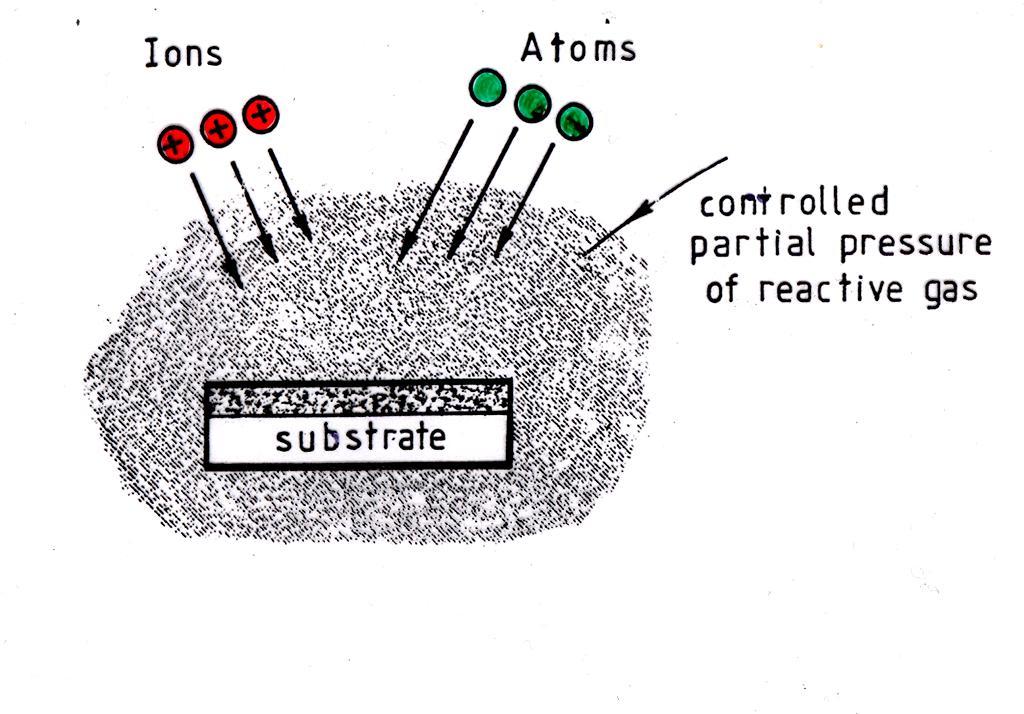
5 DUAL BEAM ION-ASSISTED DEPOSITION SYSTEM


6 Dark field images of TiN films grown at 473K


7 No ion-assist Ion-assist Effect of 50 ev Ar ion assist on microstructure of Si for Ar/Si ratio of 0.5 J.Ferron, R.R.Koropecke and R.Arce Phys.Rev. B (1986)

8 Model by R W Smith and D J Srolowitz J.Appl Phys. 79 (1996) NO ION-assist MD Simulation for 100eV Ar-Ni IAD K-H Muller Phys Rev B 35(1987) 7906
9 IS THE RULE THEREFORE eV PER ATOM WITH PREFERENCE FOR LOW ENERGY IONS? YES IN PRINCIPLE BUT THERE ARE FURTHER CONDITIONS 1. YOU REALLY NEED THE SAME NUMBER OF IONS AND COATING ATOMS ARRIVING AT THE SURFACE PER UNIT TIME (Otherwise some atoms in the coating are buried before they experience the added energy pulse) e.g. If depositing a monolayer of coating per second (about 6 x atoms/cm 2 ) you need the same ion bombardment density. 1 microamp-sec is 1 x 10⁻⁶ Coulomb. Each ion brings 1.6 x Coulomb so at 1 microamp you bring approx 6 x ions to the surface. You need 100 times this rate (100 microamp/sec) to match the arrival rate of coating particles. Many systems do not use this current density which means coating atoms are buried before they can experience added energy. Clearly, the conditions are better using the HIPIMS sputtering mode where many coating particles are ionised.
10 Density change with Oxygen ion-assistance of evaporated ZrO 2 (Note that for full film density you need 120µA/cm 2 ) P.J.Martin, H.A.MacLeod, R.P.Netterfield and W.G.Sainty Applied Optics 22, 178 (1983)
11 50/50 400eV Ar/N ions on 400 deg C substrate Park et al JVST A15 (1997) 1041
12 Effect of Ne ion/c arrival ratio and energy on the crystalline growth of diamond films K.Ogata, Y.Andoh and E.Kamijo NIMB 33 (1988)
 1360-1364 [Other data from Harper et al o-sio 2, Δ- other dielectrics, -metals, Ộ-semiconductors in Ion Bombardment Modification of Surfaces ed O.")
13 Relation between ion-assist energy and ion/atom ratio required to make significant changes in coating properties. A: SiNx, B: SiO 2, C : αc:h. Martinu et al, JVST A12 (1994) [Other data from Harper et al o-sio 2, Δ- other dielectrics, -metals, Ộ-semiconductors in Ion Bombardment Modification of Surfaces ed O.Auciello and R.Kelly. Elsevier, Amsterdam, 1984]

14 Note: you can achieve the same added energy per atom by using five 20eV ions/atom or one 100eV ion/atom but coating properties are quite different Petrov et al Ti 0.5 Al 0.5 N Phys Lett 63 (1993) p36
15 IS THE RULE THEREFORE eV PER ATOM WITH PREFERENCE FOR LOW ENERGY IONS and AT LEAST 1 ION PER DEPOSITING ATOM? YES IN PRINCIPLE BUT THERE IS A FURTHER CONDITION 2. IMPURITIES CAN MODERATE THE FILM NUCLEATION AND GROWTH Remember that, at 10-6 mbar and sticking coefficient of gas 1.0, a perfectly clean surface is completely covered with gas in 0.6 seconds
16 Impurity atoms on the surface (or even atoms of a second component of the coating) can block the diffusion and alter growth morphology
, Protective Coatings and Thin Films, Kluwer Academic Publishers, the Netherlands, 1997, p. 279. J. Musil, J. Vlček, Surf. Coat. Technol.")
17 P.B. Barna, M. Adamik, in: Y. Pauleau, P.B. Barna (Eds.), Protective Coatings and Thin Films, Kluwer Academic Publishers, the Netherlands, 1997, p J. Musil, J. Vlček, Surf. Coat. Technol (2001) 557. Example showing effect of Cu on Zr-N morphology
18 Effect of low levels of impurity on microhardness of nc TiN/a-Si 3 N 4 S. Veprek,H.-D. Maennling, A. Niederhofer, D. Ma and S. Mukherjeec JVST B 22(5) (2004) L5-L9
19 Hard nanocomposite coatings: Thermal stability, oxidation resistance and toughness J. Musil SCT 207 (2012) 50-65
 (2010) 521-530")
20 INTERNAL COATING OF TiZrV FILMS ON TUBES R.Valizadeh, O.B.Malyshev, J.S.Colligon et al. JVST A27 (3) (2010)
 2x10⁻³ mbar with DC pulsed power supply")

21 at T = 70 o C but using different working pressures (a) 10-2 mbar (b) 2x10⁻³ mbar with DC pulsed power supply NON-EVAPORABLE TiVZr COATING WITH DIFFERENT MICROSTRUCTURE R.Valizadeh, O.B.Malyshev, J.S.Colligon et al. JVST A 27 (3)(2009)
22
23 Effect of IAD and T on hardness of Ti-Si-N films N 2 /atom ratio is 1, Si content 9 at% Colligon et al TSF 485 (2005)
")
24 Ti-Si-N films with 9 at % Si formed using IAD with 400eV N 2 ions; ion/atom ratio = 1 Colligon et al TSF 485 (2005)

25 Ion beam induced deposition using 98 pa 30keV Ga and W(CO) 6 precursor. Sadki et al, Physica C (1995)
 and 1pA 30keV Ga ions Nakamatsu et al JVST B 23 (6) (2005)")
26 DLC 380nm coil dia, 130nm wire section springs using penanthrine (C14H10) and 1pA 30keV Ga ions Nakamatsu et al JVST B 23 (6) (2005)
27 DYNAMIC RECOIL MIXING By maintaining a constant thin film of material on a substrate by matching the deposition rate to the re-sputter rate atoms can be recoil implanted into the substrate. Gold was recoil implanted into PET plastic to form a sensor

28 Choose thickness of Au layer so the maximum number of collisions occurs between the gold and the substrate. During bombardment add more gold to replace exactly the amount sputtered. At the end remove surface gold and find gold remains below the substrate surface (Colligon et al, unpublished)
; (b)--- pure gold; DRM gold; (c) DRM gold lifetime response original;")
29 Electrochemical properties of DRM layers punched into PET (a) Pt in Ti (0.5M ultrar H 2 O 4 ); (b)--- pure gold; DRM gold; (c) DRM gold lifetime response original; --- after 12 weeks
 whereas 80keV Xe gives about 230 ev/å (point A).")
30 By matching the thickness of Ni on Si you can select the energy loss per Ångström at the interface for different ions and energies (e.g. 40keV Ni gives about 120eV/Å (point B) whereas 80keV Xe gives about 230 ev/å (point A). Different nickel silicides result

31 Ni-Si depth profiles formed by 80keV ion bombardment of 10nm Ni on Si. Ion dose increases going down left set from top. Horizontal lines at 0.4 and 0.6 at top right show Ni 2 Si 3 has formed Colligon et al, unpublished
32 MAX phases are of form M n+1 AX n where n is 1,2 or 3 and depends on the different stacking sequence of the MX block between the A- element layers. M is Sc, Ti, V, Cr, Zr, Nb, Mo, Hf, Ta A is group III A or IV A element Al, Si, P, S, Ga, Ge, As, Cd, In, Sn, Tl, Pb also can be Cd, P, S or As X is either C o r N Barsoum showed that highly ductile Ti 3 SiC 2 was thermal shock resistant and oxidation resistant even at temperatures in excess of 1000 o C.

33 STRUCTURE OF Ti 3 SiC 2 : L Farber and I Levin NIST
")
34 Sputter Ti (Mag 1), Si (Mag 2) and C (Mag 3) to give layer-by layer growth on rotating heated substrate V Vishnyakov, J Lu, P Eklund, L Hultman and J Colligon Vacuum 93 (2013) 56-59
 lattice image, and (c)")


35 Atomic fringes for C (a) Cross-sectional transmission electron microscopy image, (b) lattice image, and (c) corresponding selected area diffraction electron diffraction pattern from the sample deposited at 650 C. Lattice spacing c=1.77nm corresponds with the value for theti 3 SiC 2 MAX phase V Vishnyakov, J Lu, P Eklund, L Hultman and J Colligon Vacuum 93 (2013) 56-59
")
36 Ti 3 SiC 2 MAX phase V Vishnyakov, J Lu, P Eklund, J.Colligon and L Hultman et al Vacuum 93 (2013) 56-59
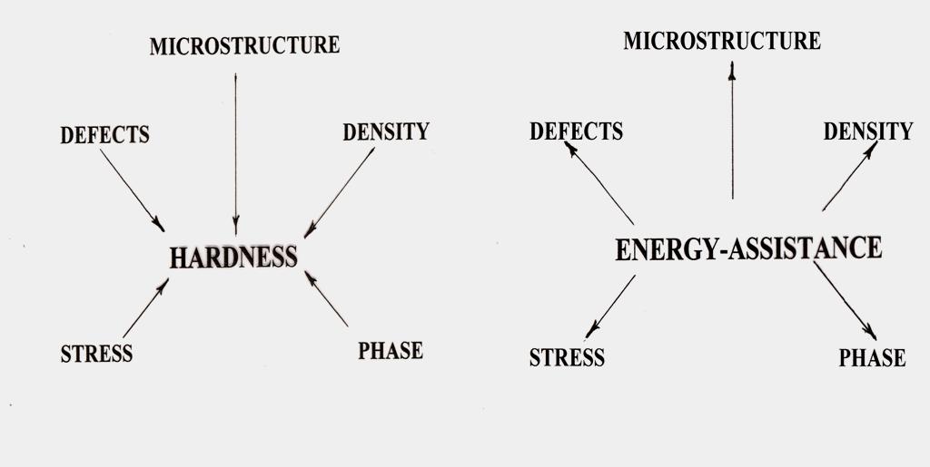
37 SUMMARY Energy-Assisted Deposition provides control of composition, phase, microstructure, stress and hence improved hardness, temperature stability, radiation resistance, wear and many other coating properties. Control of deposition conditions is essential, especially impurity content for nanoscale microstructure coatings. In general added energy per atom deposited needs to be of the order ev per atom and ion energy about 20-30eV New developing areas include MAX phases and 2D Maxene Commercial potential is significant with the world output of products with coatings already exceeding 80 Billion US Dollars per annum
38 My thanks to many colleagues who have worked with me over the years, in particular Reza Valizadeh, Vladimir Vishnyakov and Hamid Kheyrandish. Thanks also to the UK funding bodies EPSRC and STFC for valuable support Last but not least THANK YOU
Fabrication Technology, Part I
 EEL5225: Principles of MEMS Transducers (Fall 2004) Fabrication Technology, Part I Agenda: Microfabrication Overview Basic semiconductor devices Materials Key processes Oxidation Thin-film Deposition Reading:
High Accuracy EUV Reflectometry and Scattering at the Advanced Light Source
 High Accuracy EUV Reflectometry and Scattering at the Advanced Light Source Eric Gullikson Lawrence Berkeley National Laboratory 1 Reflectometry and Scattering Beamline (ALS 6.3.2) Commissioned Fall 1994
Ion Implant Part 1. Saroj Kumar Patra, TFE4180 Semiconductor Manufacturing Technology. Norwegian University of Science and Technology ( NTNU )
") 1 Ion Implant Part 1 Chapter 17: Semiconductor Manufacturing Technology by M. Quirk & J. Serda Spring Semester 2014 Saroj Kumar Patra,, Norwegian University of Science and Technology ( NTNU ) 2 Objectives
1 Ion Implant Part 1 Chapter 17: Semiconductor Manufacturing Technology by M. Quirk & J. Serda Spring Semester 2014 Saroj Kumar Patra,, Norwegian University of Science and Technology ( NTNU ) 2 Objectives
Non-Evaporable Getters
 Non-Evaporable Getters Dr. Oleg B. Malyshev Senior Vacuum Scientist ASTeC Vacuum Science Group, STFC Daresbury Laboratory, UK VS-2, 18-19 October 2011, Ricoh Arena, Coventry 1 Sorption and diffusion Gas
Plasma Deposition (Overview) Lecture 1
 Lecture 1") Plasma Deposition (Overview) Lecture 1 Material Processes Plasma Processing Plasma-assisted Deposition Implantation Surface Modification Development of Plasma-based processing Microelectronics needs (fabrication
Plasma Deposition (Overview) Lecture 1 Material Processes Plasma Processing Plasma-assisted Deposition Implantation Surface Modification Development of Plasma-based processing Microelectronics needs (fabrication
PART 1 Introduction to Theory of Solids
 Elsevier UK Job code: MIOC Ch01-I044647 9-3-2007 3:03p.m. Page:1 Trim:165 240MM TS: Integra, India PART 1 Introduction to Theory of Solids Elsevier UK Job code: MIOC Ch01-I044647 9-3-2007 3:03p.m. Page:2
Some more equations describing reactive magnetron sputtering.
 Some more equations describing reactive magnetron sputtering D. Depla, S. Mahieu, W. Leroy, K. Van Aeken, J. Haemers, R. De Gryse www.draft.ugent.be discharge voltage (V) 44 4 36 32 28..5 1. 1.5 S (Pumping
Introduction to X-ray Photoelectron Spectroscopy (XPS) XPS which makes use of the photoelectric effect, was developed in the mid-1960
 XPS which makes use of the photoelectric effect, was developed in the mid-1960") Introduction to X-ray Photoelectron Spectroscopy (XPS) X-ray Photoelectron Spectroscopy (XPS), also known as Electron Spectroscopy for Chemical Analysis (ESCA) is a widely used technique to investigate
Introduction to X-ray Photoelectron Spectroscopy (XPS) X-ray Photoelectron Spectroscopy (XPS), also known as Electron Spectroscopy for Chemical Analysis (ESCA) is a widely used technique to investigate
Review of Semiconductor Fundamentals
 ECE 541/ME 541 Microelectronic Fabrication Techniques Review of Semiconductor Fundamentals Zheng Yang (ERF 3017, email: yangzhen@uic.edu) Page 1 Semiconductor A semiconductor is an almost insulating material,
Interaction of ion beams with matter
 Interaction of ion beams with matter Introduction Nuclear and electronic energy loss Radiation damage process Displacements by nuclear stopping Defects by electronic energy loss Defect-free irradiation
Nova 600 NanoLab Dual beam Focused Ion Beam IITKanpur
 Nova 600 NanoLab Dual beam Focused Ion Beam system @ IITKanpur Dual Beam Nova 600 Nano Lab From FEI company (Dual Beam = SEM + FIB) SEM: The Electron Beam for SEM Field Emission Electron Gun Energy : 500
Secondary ion mass spectrometry (SIMS)
") Secondary ion mass spectrometry (SIMS) ELEC-L3211 Postgraduate Course in Micro and Nanosciences Department of Micro and Nanosciences Personal motivation and experience on SIMS Offers the possibility to
Secondary ion mass spectrometry (SIMS) ELEC-L3211 Postgraduate Course in Micro and Nanosciences Department of Micro and Nanosciences Personal motivation and experience on SIMS Offers the possibility to
Electron Rutherford Backscattering, a versatile tool for the study of thin films
 Electron Rutherford Backscattering, a versatile tool for the study of thin films Maarten Vos Research School of Physics and Engineering Australian National University Canberra Australia Acknowledgements:
Reduced preferential sputtering of TiO 2 (and Ta 2 O 5 ) thin films through argon cluster ion bombardment.
 thin films through argon cluster ion bombardment.") NATIOMEM Reduced preferential sputtering of TiO 2 (and Ta 2 O 5 ) thin films through argon cluster ion bombardment. R. Grilli *, P. Mack, M.A. Baker * * University of Surrey, UK ThermoFisher Scientific
NATIOMEM Reduced preferential sputtering of TiO 2 (and Ta 2 O 5 ) thin films through argon cluster ion bombardment. R. Grilli *, P. Mack, M.A. Baker * * University of Surrey, UK ThermoFisher Scientific
The Periodic Table of Elements
 The Periodic Table of Elements 8 Uuo Uus Uuh (9) Uup (88) Uuq (89) Uut (8) Uub (8) Rg () 0 Ds (9) 09 Mt (8) 08 Hs (9) 0 h () 0 Sg () 0 Db () 0 Rf () 0 Lr () 88 Ra () 8 Fr () 8 Rn () 8 At (0) 8 Po (09)
Atoms and the Periodic Table
 Atoms and the Periodic Table Parts of the Atom Proton Found in the nucleus Number of protons defines the element Charge +1, mass 1 Parts of the Atom Neutron Found in the nucleus Stabilizes the nucleus
X-Ray Photoelectron Spectroscopy (XPS) Prof. Paul K. Chu
 Prof. Paul K. Chu") X-Ray Photoelectron Spectroscopy (XPS) Prof. Paul K. Chu X-ray Photoelectron Spectroscopy Introduction Qualitative analysis Quantitative analysis Charging compensation Small area analysis and XPS imaging
X-Ray Photoelectron Spectroscopy (XPS) Prof. Paul K. Chu X-ray Photoelectron Spectroscopy Introduction Qualitative analysis Quantitative analysis Charging compensation Small area analysis and XPS imaging
DEPOSITION OF THIN TiO 2 FILMS BY DC MAGNETRON SPUTTERING METHOD
 Chapter 4 DEPOSITION OF THIN TiO 2 FILMS BY DC MAGNETRON SPUTTERING METHOD 4.1 INTRODUCTION Sputter deposition process is another old technique being used in modern semiconductor industries. Sputtering
CLASS TEST GRADE 11. PHYSICAL SCIENCES: CHEMISTRY Test 4: Matter and materials 1
 CLASS TEST GRADE PHYSICAL SCIENCES: CHEMISTRY Test 4: Matter and materials MARKS: 45 TIME: hour INSTRUCTIONS AND INFORMATION. Answer ALL the questions. 2. You may use non-programmable calculators. 3. You
6.5 Optical-Coating-Deposition Technologies
 92 Chapter 6 6.5 Optical-Coating-Deposition Technologies The coating process takes place in an evaporation chamber with a fully controlled system for the specified requirements. Typical systems are depicted
LOW-TEMPERATURE Si (111) HOMOEPITAXY AND DOPING MEDIATED BY A MONOLAYER OF Pb
 HOMOEPITAXY AND DOPING MEDIATED BY A MONOLAYER OF Pb") LOW-TEMPERATURE Si (111) HOMOEPITAXY AND DOPING MEDIATED BY A MONOLAYER OF Pb O.D. DUBON, P.G. EVANS, J.F. CHERVINSKY, F. SPAEPEN, M.J. AZIZ, and J.A. GOLOVCHENKO Division of Engineering and Applied Sciences,
LOW-TEMPERATURE Si (111) HOMOEPITAXY AND DOPING MEDIATED BY A MONOLAYER OF Pb O.D. DUBON, P.G. EVANS, J.F. CHERVINSKY, F. SPAEPEN, M.J. AZIZ, and J.A. GOLOVCHENKO Division of Engineering and Applied Sciences,
ToF-SIMS or XPS? Xinqi Chen Keck-II
 ToF-SIMS or XPS? Xinqi Chen Keck-II 1 Time of Flight Secondary Ion Mass Spectrometry (ToF-SIMS) Not ToF MS (laser, solution) X-ray Photoelectron Spectroscopy (XPS) 2 3 Modes of SIMS 4 Secondary Ion Sputtering
Imaging Methods: Scanning Force Microscopy (SFM / AFM)
") Imaging Methods: Scanning Force Microscopy (SFM / AFM) The atomic force microscope (AFM) probes the surface of a sample with a sharp tip, a couple of microns long and often less than 100 Å in diameter.
Imaging Methods: Scanning Force Microscopy (SFM / AFM) The atomic force microscope (AFM) probes the surface of a sample with a sharp tip, a couple of microns long and often less than 100 Å in diameter.
single-layer transition metal dichalcogenides MC2
 single-layer transition metal dichalcogenides MC2 Period 1 1 H 18 He 2 Group 1 2 Li Be Group 13 14 15 16 17 18 B C N O F Ne 3 4 Na K Mg Ca Group 3 4 5 6 7 8 9 10 11 12 Sc Ti V Cr Mn Fe Co Ni Cu Zn Al Ga
Carbon Nanotubes in Interconnect Applications
 Carbon Nanotubes in Interconnect Applications Page 1 What are Carbon Nanotubes? What are they good for? Why are we interested in them? - Interconnects of the future? Comparison of electrical properties
Energy fluxes in plasmas for fabrication of nanostructured materials
 Energy fluxes in plasmas for fabrication of nanostructured materials IEAP, Universität Kiel 2nd Graduate Summer Institute "Complex Plasmas" August 5-13, 2010 in Greifswald (Germany) AG 1 Outline Motivation
materials and their properties
 materials and their properties macroscopic properties phase state strength / stiffness electrical conductivity chemical properties color / transparence spectroscopical properties surface properties density
EE143 Fall 2016 Microfabrication Technologies. Lecture 6: Thin Film Deposition Reading: Jaeger Chapter 6
 EE143 Fall 2016 Microfabrication Technologies Lecture 6: Thin Film Deposition Reading: Jaeger Chapter 6 Prof. Ming C. Wu wu@eecs.berkeley.edu 511 Sutardja Dai Hall (SDH) 1 Vacuum Basics Units 1 atmosphere
SUPPLEMENTARY MATERIALS FOR PHONON TRANSMISSION COEFFICIENTS AT SOLID INTERFACES
 148 A p p e n d i x D SUPPLEMENTARY MATERIALS FOR PHONON TRANSMISSION COEFFICIENTS AT SOLID INTERFACES D.1 Overview The supplementary information contains additional information on our computational approach
FIB - SIMS. Focussed Ion Beam Secondary Ion Mass Spectrometry.
 FIB - SIMS Focussed Ion Beam Secondary Ion Mass Spectrometry Outline Introduction to Hiden Analytical Introduction to SIMS FIB-SIMS - Introduction and key features FIB-SIMS - Applications data Hiden SIMS
Atomic Physics. Chapter 6 X ray. Jinniu Hu 24/12/ /20/13
 Atomic Physics Chapter 6 X ray 11/20/13 24/12/2018 Jinniu Hu 1!1 6.1 The discovery of X ray X-rays were discovered in 1895 by the German physicist Wilhelm Roentgen. He found that a beam of high-speed electrons
Modification of Thin Film Properties by Sputtered Particles
 1 Modification of Thin Film Properties by Sputtered Particles Yasunori Taga 1. Introduction The novelty of the functions provided by plasma-assisted physical vapor deposition films, together with their
Atomic Structure & Interatomic Bonding
 Atomic Structure & Interatomic Bonding Chapter Outline Review of Atomic Structure Atomic Bonding Atomic Structure Atoms are the smallest structural units of all solids, liquids & gases. Atom: The smallest
Supplementary Figure S1. AFM characterizations and topographical defects of h- BN films on silica substrates. (a) (c) show the AFM height
 (c) show the AFM height") Supplementary Figure S1. AFM characterizations and topographical defects of h- BN films on silica substrates. (a) (c) show the AFM height topographies of h-bn film in a size of ~1.5µm 1.5µm, 30µm 30µm
Supplementary Figure S1. AFM characterizations and topographical defects of h- BN films on silica substrates. (a) (c) show the AFM height topographies of h-bn film in a size of ~1.5µm 1.5µm, 30µm 30µm
Surface and Interface Characterization of Polymer Films
 Surface and Interface Characterization of Polymer Films Jeff Shallenberger, Evans Analytical Group 104 Windsor Center Dr., East Windsor NJ Copyright 2013 Evans Analytical Group Outline Introduction to
NAME: FIRST EXAMINATION
 1 Chemistry 64 Winter 1994 NAME: FIRST EXAMINATION THIS EXAMINATION IS WORTH 100 POINTS AND CONTAINS 4 (FOUR) QUESTIONS THEY ARE NOT EQUALLY WEIGHTED! YOU SHOULD ATTEMPT ALL QUESTIONS AND ALLOCATE YOUR
CHAPTER 6: Etching. Chapter 6 1
 Chapter 6 1 CHAPTER 6: Etching Different etching processes are selected depending upon the particular material to be removed. As shown in Figure 6.1, wet chemical processes result in isotropic etching
Honors Chemistry - Unit 4 Bonding Part I
 Honors Chemistry - Unit 4 Bonding Part I Unit 4 Packet - Page 1 of 8 Vocab Due: Quiz Date(s): Test Date: UT Quest Due: Bonding Vocabulary: see separate handout assignment OBJECTIVES: Chapters 4-8 Be able
Ion Implantation ECE723
 Ion Implantation Topic covered: Process and Advantages of Ion Implantation Ion Distribution and Removal of Lattice Damage Simulation of Ion Implantation Range of Implanted Ions Ion Implantation is the
Section 5: Thin Film Deposition part 1 : sputtering and evaporation. Jaeger Chapter 6. EE143 Ali Javey
 Section 5: Thin Film Deposition part 1 : sputtering and evaporation Jaeger Chapter 6 Vacuum Basics 1. Units 1 atmosphere = 760 torr = 1.013x10 5 Pa 1 bar = 10 5 Pa = 750 torr 1 torr = 1 mm Hg 1 mtorr =
3.155J/6.152J Microelectronic Processing Technology Fall Term, 2004
 3.155J/6.152J Microelectronic Processing Technology Fall Term, 2004 Bob O'Handley Martin Schmidt Quiz Nov. 17, 2004 Ion implantation, diffusion [15] 1. a) Two identical p-type Si wafers (N a = 10 17 cm
CHEMICAL COMPOUNDS MOLECULAR COMPOUNDS
 48 CHEMICAL COMPOUNDS - Dalton's theory does not mention this, but there is more than one way for atoms to come together to make chemical compounds! - There are TWO common kinds of chemical compound, classified
Secondaryionmassspectrometry
 Secondaryionmassspectrometry (SIMS) 1 Incident Ion Techniques for Surface Composition Analysis Mass spectrometric technique 1. Ionization -Electron ionization (EI) -Chemical ionization (CI) -Field ionization
This is an author produced version of a paper presented at 2nd PATCMC, June 6th-8th 2011 Plzeň, Czech Republic.
 http://uu.diva-portal.org This is an author produced version of a paper presented at 2nd PATCMC, June 6th-8th 2011 Plzeň, Czech Republic. Kubart, T. 2011. Process modelling for reactive magnetron sputtering
SCIENCE 1206 UNIT 2 CHEMISTRY. September 2017 November 2017
 SCIENCE 1206 UNIT 2 CHEMISTRY September 2017 November 2017 UNIT OUTLINE 1. Review of Grade 9 Terms & the Periodic Table Bohr diagrams Evidence for chemical reactions Chemical Tests 2. Naming & writing
Chemistry 31A Autumn 2004 Professors Chidsey & Zare Exam 2 Name:
 Chemistry 31A Autumn 2004 Professors Chidsey & Zare Exam 2 Name: SUNetID: @stanford.edu Honor Code Observed: (Signature) Circle your section 9:00am 10:00am 2:15pm 3:15pm 7:00pm 8:00pm S02 OC103 S04 OC103
Fig 1: Auger Electron Generation (a) Step 1 and (b) Step 2
 Step 1 and (b) Step 2") Auger Electron Spectroscopy (AES) Physics of AES: Auger Electrons were discovered in 1925 but were used in surface analysis technique in 1968. Auger Electron Spectroscopy (AES) is a very effective method
Auger Electron Spectroscopy (AES) Physics of AES: Auger Electrons were discovered in 1925 but were used in surface analysis technique in 1968. Auger Electron Spectroscopy (AES) is a very effective method
Last 4 Digits of USC ID:
 Chemistry 05 B Practice Exam Dr. Jessica Parr First Letter of last Name PLEASE PRINT YOUR NAME IN BLOCK LETTERS Name: Last 4 Digits of USC ID: Lab TA s Name: Question Points Score Grader 8 2 4 3 9 4 0
PHYSICAL SCIENCES MARCH CONTROLLED TEST GRADE
 PHYSICAL SCIENCES MARCH CONTROLLED TEST GRADE 11 018 MARKS : 75 TIME : 1.5 Hrs INSTRUCTIONS AND INFORMATION 1. Write your NAME and CLASS in your ANSWER BOOK.. This question paper consists of SIX questions.
TMT4320 Nanomaterials November 10 th, Thin films by physical/chemical methods (From chapter 24 and 25)
") 1 TMT4320 Nanomaterials November 10 th, 2015 Thin films by physical/chemical methods (From chapter 24 and 25) 2 Thin films by physical/chemical methods Vapor-phase growth (compared to liquid-phase growth)
1 TMT4320 Nanomaterials November 10 th, 2015 Thin films by physical/chemical methods (From chapter 24 and 25) 2 Thin films by physical/chemical methods Vapor-phase growth (compared to liquid-phase growth)
Chemistry 1 First Lecture Exam Fall Abbasi Khajo Levine Mathias Mathias/Ortiz Metlitsky Rahi Sanchez-Delgado Vasserman
 Chemistry 1 First Lecture Exam Fall 2011 Page 1 of 9 NAME Circle the name of your recitation/lab instructor(s) Abbasi Khajo Levine Mathias Mathias/Ortiz Metlitsky Rahi Sanchez-Delgado Vasserman Before
100% ionic compounds do not exist but predominantly ionic compounds are formed when metals combine with non-metals.
 2.21 Ionic Bonding 100% ionic compounds do not exist but predominantly ionic compounds are formed when metals combine with non-metals. Forming ions Metal atoms lose electrons to form +ve ions. Non-metal
UV LED charge control of an electrically isolated proof mass at 255 nm
 UV LED charge control of an electrically isolated proof mass at 255 nm Karthik Balakrishnan Department of Aeronautics and Astronautics Hansen Experimental Physics Labs Stanford University karthikb@stanford.edu
Soft X-ray multilayer mirrors by ion assisted sputter deposition
 Soft X-ray multilayer mirrors by ion assisted sputter deposition Valentino Rigato INFN Laboratori Nazionali di Legnaro Bologna, September 21, 2010 Source: INFN-LNL-2009 V. RIGATO 1 SIF- Bologna September
CHEMICAL COMPOUNDS MOLECULAR COMPOUNDS
 48 CHEMICAL COMPOUNDS - Dalton's theory does not mention this, but there is more than one way for atoms to come together to make chemical compounds! - There are TWO common kinds of chemical compound, classified
Chapter 3: Stoichiometry
 Chapter 3: Stoichiometry Chem 6A Michael J. Sailor, UC San Diego 1 Announcements: Thursday (Sep 29) quiz: Bring student ID or we cannot accept your quiz! No notes, no calculators Covers chapters 1 and
ORBITAL DIAGRAM - A graphical representation of the quantum number "map" of electrons around an atom.
 178 (MAGNETIC) SPIN QUANTUM NUMBER: "spin down" or "spin up" - An ORBITAL (region with fixed "n", "l" and "ml" values) can hold TWO electrons. ORBITAL DIAGRAM - A graphical representation of the quantum
Unit 1 Part 2 Atomic Structure and The Periodic Table Introduction to the Periodic Table UNIT 1 ATOMIC STRUCTURE AND THE PERIODIC TABLE
 UNIT 1 ATOMIC STRUCTURE AND THE PERIODIC TABLE PART 2 INTRODUCTION TO THE PERIODIC TABLE Contents 1. The Structure of the Periodic Table 2. Trends in the Periodic Table Key words: group, period, block,
Effect of Spiral Microwave Antenna Configuration on the Production of Nano-crystalline Film by Chemical Sputtering in ECR Plasma
 THE HARRIS SCIENCE REVIEW OF DOSHISHA UNIVERSITY, VOL. 56, No. 1 April 2015 Effect of Spiral Microwave Antenna Configuration on the Production of Nano-crystalline Film by Chemical Sputtering in ECR Plasma
7) Applications of Nuclear Radiation in Science and Technique (1) Analytical applications (Radiometric titration)
 Applications of Nuclear Radiation in Science and Technique (1) Analytical applications (Radiometric titration)") 7) Applications of Nuclear Radiation in Science and Technique (1) (Radiometric titration) The radioactive material is indicator Precipitation reactions Complex formation reactions Principle of a precipitation
7) Applications of Nuclear Radiation in Science and Technique (1) (Radiometric titration) The radioactive material is indicator Precipitation reactions Complex formation reactions Principle of a precipitation
M. Audronis 1 and F. Zimone 2 1. Nova Fabrica Ltd. 1. Angstrom Sciences Inc.
 M. Audronis 1 and F. Zimone 2 1 Nova Fabrica Ltd. 1 Angstrom Sciences Inc. Email: info@novafabrica.biz 1 Founded in 2013 the company is based in Lithuania (northern EU). NF are involved in two business
Lecture 9: Metal-semiconductor junctions
 Lecture 9: Metal-semiconductor junctions Contents 1 Introduction 1 2 Metal-metal junction 1 2.1 Thermocouples.......................... 2 3 Schottky junctions 4 3.1 Forward bias............................
 lectures accompanying the book: Solid State Physics: An Introduction, by Philip ofmann (2nd edition 2015, ISBN-10: 3527412824, ISBN-13: 978-3527412822, Wiley-VC Berlin. www.philiphofmann.net 1 Bonds between
Chapter III: III: Sputtering and secondary electron emission
 References [1] Handbook of putter deposition technology, Kiyotaka Wasa, Noyes publications, NJ 1992. IN: 0-8155-1280-5 [2] old Plasma in Materials Fabrications,. Grill, IEEE Press, NY(1993). IN: 0-7803-1055-1.
In search for the limits of
 In search for the limits of rotating cylindrical magnetron sputtering W. P. Leroy, S. Mahieu, R. De Gryse, D. Depla DRAFT Dept. Solid State Sciences Ghent University Belgium www.draft.ugent.be Planar Magnetron
The University of Alabama 1 st APT Workshop for Earth Sciences
 The University of Alabama 1 st APT Workshop for Earth Sciences January 2016 David Reinhard LEAP 5000 www.cameca.com Microstructure characterization technique (UHV) that uses field evaporation (high electric
ION BOMBARDMENT CHARACTERISTICS DURING THE GROWTH OF OPTICAL FILMS USING A COLD CATHODE ION SOURCE
 ION BOMBARDMENT CHARACTERISTICS DURING THE GROWTH OF OPTICAL FILMS USING A COLD CATHODE ION SOURCE O. Zabeida, J.E. Klemberg-Sapieha, and L. Martinu, Ecole Polytechnique, Department of Engineering Physics
CHEM 10113, Quiz 5 October 26, 2011
 CHEM 10113, Quiz 5 October 26, 2011 Name (please print) All equations must be balanced and show phases for full credit. Significant figures count, show charges as appropriate, and please box your answers!
CHEM 130 Exp. 8: Molecular Models
 CHEM 130 Exp. 8: Molecular Models In this lab, we will learn and practice predicting molecular structures from molecular formulas. The Periodic Table of the Elements IA 1 H IIA IIIA IVA VA VIA VIIA 3 5
VIIIA H PREDICTING CHARGE
 58 IA PREDICTING CHARGE VIIIA H IIA IIIA IVA VA VIA VIIA You can reliably determine the charge using our method for Groups IA, IIA, IIIB, Aluminum, and the Group VA, VIA, and VIIA NONMETALS Li Be B C N
Unique phenomena of tungsten associated with fusion reactor: uncertainties of stable hydrogen configuration tapped in tungsten vacancy
 Unique phenomena of tungsten associated with fusion reactor: uncertainties of stable hydrogen configuration tapped in tungsten vacancy Kyushu University Kazuhito Ohsawa Technical Meeting of the International
Lab Day and Time: Instructions. 1. Do not open the exam until you are told to start.
 Name: Lab Day and Time: Instructions 1. Do not open the exam until you are told to start. 2. This exam is closed note and closed book. You are not allowed to use any outside material while taking this
Guide to the Extended Step-Pyramid Periodic Table
 Guide to the Extended Step-Pyramid Periodic Table William B. Jensen Department of Chemistry University of Cincinnati Cincinnati, OH 452201-0172 The extended step-pyramid table recognizes that elements
Electrons. Unit H Chapter 6
 Electrons Unit H Chapter 6 1 Electrons were discovered by 1. Dalton 2. Lavoisier 3. Proust 4. Mendeleev 6. Rutherford 7. Bohr 8. Schrodinger 9. Dirac 5. Thomson 2 Electrons were discovered by 1. Dalton
Surface analysis techniques
 Experimental methods in physics Surface analysis techniques 3. Ion probes Elemental and molecular analysis Jean-Marc Bonard Academic year 10-11 3. Elemental and molecular analysis 3.1.!Secondary ion mass
A novel sputtering technique: Inductively Coupled Impulse Sputtering (ICIS)
") IOP Conference Series: Materials Science and Engineering A novel sputtering technique: Inductively Coupled Impulse Sputtering (ICIS) To cite this article: D A L Loch and A P Ehiasarian 2012 IOP Conf. Ser.:
IOP Conference Series: Materials Science and Engineering A novel sputtering technique: Inductively Coupled Impulse Sputtering (ICIS) To cite this article: D A L Loch and A P Ehiasarian 2012 IOP Conf. Ser.:
Spin-resolved photoelectron spectroscopy
 Spin-resolved photoelectron spectroscopy Application Notes Spin-resolved photoelectron spectroscopy experiments were performed in an experimental station consisting of an analysis and a preparation chamber.
5 questions, 3 points each, 15 points total possible. 26 Fe Cu Ni Co Pd Ag Ru 101.
 Physical Chemistry II Lab CHEM 4644 spring 2017 final exam KEY 5 questions, 3 points each, 15 points total possible h = 6.626 10-34 J s c = 3.00 10 8 m/s 1 GHz = 10 9 s -1. B= h 8π 2 I ν= 1 2 π k μ 6 P
The Periodic Table. Periodic Properties. Can you explain this graph? Valence Electrons. Valence Electrons. Paramagnetism
 Periodic Properties Atomic & Ionic Radius Energy Electron Affinity We want to understand the variations in these properties in terms of electron configurations. The Periodic Table Elements in a column
CHEMICAL COMPOUNDS. - Dalton's theory does not mention this, but there is more than one way for atoms to come together to make chemical compounds!
 69 CHEMICAL COMPOUNDS - Dalton's theory does not mention this, but there is more than one way for atoms to come together to make chemical compounds! - There are TWO common kinds of chemical compound, classified
NITROGEN CONTAINING ULTRA THIN SiO 2 FILMS ON Si OBTAINED BY ION IMPLANTATION
 NITROGEN CONTAINING ULTRA THIN SiO 2 FILMS ON Si OBTAINED BY ION IMPLANTATION Sashka Petrova Alexandrova 1, Evgenia Petrova Valcheva 2, Rumen Georgiev Kobilarov 1 1 Department of Applied Physics, Technical
A semiconductor is an almost insulating material, in which by contamination (doping) positive or negative charge carriers can be introduced.
 positive or negative charge carriers can be introduced.") Semiconductor A semiconductor is an almost insulating material, in which by contamination (doping) positive or negative charge carriers can be introduced. Page 2 Semiconductor materials Page 3 Energy levels
Semiconductor A semiconductor is an almost insulating material, in which by contamination (doping) positive or negative charge carriers can be introduced. Page 2 Semiconductor materials Page 3 Energy levels
02/05/09 Last 4 Digits of USC ID: Dr. Jessica Parr
 Chemistry 05 B First Letter of PLEASE PRINT YOUR NAME IN BLOCK LETTERS Exam last Name Name: 02/05/09 Last 4 Digits of USC ID: Dr. Jessica Parr Lab TA s Name: Question Points Score Grader 2 2 9 3 9 4 2
High-density data storage: principle
 High-density data storage: principle Current approach High density 1 bit = many domains Information storage driven by domain wall shifts 1 bit = 1 magnetic nanoobject Single-domain needed Single easy axis
1. Following Dalton s Atomic Theory, 2. In 1869 Russian chemist published a method. of organizing the elements. Mendeleev showed that
 20 CHEMISTRY 11 D. Organizing the Elements The Periodic Table 1. Following Dalton s Atomic Theory, By 1817, chemists had discovered 52 elements and by 1863 that number had risen to 62. 2. In 1869 Russian
Circle the letters only. NO ANSWERS in the Columns!
 Chemistry 1304.001 Name (please print) Exam 5 (100 points) April 18, 2018 On my honor, I have neither given nor received unauthorized aid on this exam. Signed Date Circle the letters only. NO ANSWERS in
8. Relax and do well.
 CHEM 1215 Exam III John III. Gelder November 11, 1998 Name TA's Name Lab Section INSTRUCTIONS: 1. This examination consists of a total of 7 different pages. The last page includes a periodic table and
Deposition of thin films
 16 th March 2011 The act of applying a thin film to a surface is thin-film deposition - any technique for depositing a thin film of material onto a substrate or onto previously deposited layers. Thin is
Crystals Statics. Structural Properties. Geometry of lattices. Aug 23, 2018
 Crystals Statics. Structural Properties. Geometry of lattices Aug 23, 2018 Crystals Why (among all condensed phases - liquids, gases) look at crystals? We can take advantage of the translational symmetry,
Nucleus. Electron Cloud
 Atomic Structure I. Picture of an Atom Nucleus Electron Cloud II. Subatomic particles Particle Symbol Charge Relative Mass (amu) protons p + +1 1.0073 neutrons n 0 1.0087 electrons e - -1 0.00054858 Compare
CHEMICAL COMPOUNDS MOLECULAR COMPOUNDS
 48 CHEMICAL COMPOUNDS - Dalton's theory does not mention this, but there is more than one way for atoms to come together to make chemical compounds! - There are TWO common kinds of chemical compound, classified
Element Cube Project (x2)
") Element Cube Project (x2) Background: As a class, we will construct a three dimensional periodic table by each student selecting two elements in which you will need to create an element cube. Helpful Links
Element Cube Project (x2) Background: As a class, we will construct a three dimensional periodic table by each student selecting two elements in which you will need to create an element cube. Helpful Links
Plasma processes under low and atmospheric pressure.
 Plasma processes under low and atmospheric pressure. O.Kylián, J. Hanuš, A. Choukourov, J. Kousal, A. Kuzminova, P. Solar, A. Shelemin, H. Biederman Charles University in Prague Faculty of Mathematics
X-ray photoelectron spectroscopic characterization of molybdenum nitride thin films
 Korean J. Chem. Eng., 28(4), 1133-1138 (2011) DOI: 10.1007/s11814-011-0036-2 INVITED REVIEW PAPER X-ray photoelectron spectroscopic characterization of molybdenum nitride thin films Jeong-Gil Choi Department
PART CHAPTER2. Atomic Bonding
 PART O N E APTER2 Atomic Bonding The scanning tunneling microscope (Section 4.7) allows the imaging of individual atoms bonded to a material surface. In this case, the microscope was also used to manipulate
Supporting Data. The University of Texas at Dallas, 800 West Campbell Road, Richardson, Texas 75080, United
 Supporting Data MoS 2 Functionalization for Ultra-thin Atomic Layer Deposited Dielectrics Angelica Azcatl, 1 Stephen McDonnell, 1 Santosh KC, 1 Xing Peng, 1 Hong Dong, 1 Xiaoye Qin, 1 Rafik Addou, 1 Greg
CHEM 167 FINAL EXAM MONDAY, MAY 2 9:45 11:45 A.M GILMAN HALL
 PROF. JOHN VERKADE SPRING 2005 THIS EXAM CONSISTS OF 12 QUESTIONS ON 9 PAGES CHEM 167 HOUR EXAM IV APRIL 20, 2005 SEAT NO. NAME RECIT. INSTR. RECIT. SECT. GRADING PAGE Page 2 Page 3 Page 4 Page 5 Page
Instructions. 1. Do not open the exam until you are told to start.
 Name: Lab Day and Time: Instructions 1. Do not open the exam until you are told to start. 2. This exam is closed note and closed book. You are not allowed to use any outside material while taking this
Accelerated Neutral Atom Beam (ANAB)
") Accelerated Neutral Atom Beam (ANAB) Development and Commercialization July 2015 1 Technological Progression Sometimes it is necessary to develop a completely new tool or enabling technology to meet future
Accelerated Neutral Atom Beam (ANAB) Development and Commercialization July 2015 1 Technological Progression Sometimes it is necessary to develop a completely new tool or enabling technology to meet future
DEPOSITION AND COMPOSITION OF POLYMER FILMS IN FLUOROCARBON PLASMAS*
 DEPOSITION AND COMPOSITION OF POLYMER FILMS IN FLUOROCARBON PLASMAS* Kapil Rajaraman and Mark J. Kushner 1406 W. Green St. Urbana, IL 61801 rajaramn@uiuc.edu mjk@uiuc.edu http://uigelz.ece.uiuc.edu November