experiment (DOE) is performed to characterize the effect of ICP power, RIE power,
|
|
|
- Prosper White
- 6 years ago
- Views:
Transcription
1 Characterization of a 10 μm/min chlorine-based ICP etch process for GaAs vias R.J. Westerman, D.J. Johnson, Y.S. Lee Unaxis USA, Inc., St. Petersburg, Florida Abstract The development of a 10μm/min etch process for the definition of backside vias in GaAs is described. GaAs etch rates as high as 15.5μm/min are reported. A designed experiment (DOE) is performed to characterize the effect of ICP power, RIE power, fraction of Cl 2, and pressure on the GaAs etch rate, selectivity to photo-resist and etched via profile. A high chlorine flow rate is used and in this regime it is found that GaAs etch rate is primarily a function of ICP power, indicating that dissociation of Cl 2 to Cl is the rate limiting step. Selectivity to photo resist is found to be only a function of bias power, providing an independent control of via slope when a sloped resist mask is employed. The variation of etch rate with via diameter is also reported. Introduction GaAs devices are used extensively in the wireless telecommunications industry, where the high electron mobility of GaAs makes it well suited for high frequency, low noise, high gain applications. Although it has excellent electrical properties, GaAs is a relatively poor thermal conductor, making it difficult to remove heat efficiently from
2 power devices. A commonly used solution to this issue is the formation of vias from the wafer backside to the frontside circuitry. Such vias provide a good thermal path for heat removal as well as a low impedance ground. Backside via formation is one of the final steps in the device fabrication. After completion of the frontside processing, the wafer is mounted face down on a carrier wafer and mechanically thinned to a thickness of approximately 100 microns. The back of the wafer is then patterned using photo-resist and the vias are plasma etched through the thinned substrate, stopping on the frontside metal. After resist removal the vias are metallized, typically by sputtering a gold seed layer followed by an electroless gold plating to act as the heat sink / ground connection. A manufacturable backside via etch process is subject to a number of constraints: Short process time the etch process is required to etch vias 60 microns in diameter by 100 microns deep. A typical via etch at 6 μm/min results in etch times of 17 minutes per wafer. High GaAs:Stop Metal etch selectivity since the thinning process can result in thickness variations of several microns, it is imperative that the via etch process not damage or etch the underlying frontside metal contact High GaAs:Resist etch selectivity the via etch process is typically required to etch through a 100 micron GaAs layer. GaAs:Resist selectivities greater than 10:1 are
3 necessary to keep the required photoresist thicknesses under 14 microns the maximum resist thickness typically achievable in a single spin. Excellent etch rate uniformity a highly uniform etch reduces the need for extensive overetches reducing the overall process time Result in a via with good electrical properties in order to achieve good electrical properties, the resultant via must be compatible with the downstream metallization capabilities. Sloping the via profile during the etch process reduces the effective aspect ratio of the via which facilitates metallization Robust process the via etch should be insensitive to upstream (grind & lithography) process variations as well as feed material (substrate type). Etching of GaAs through wafer vias for backside contact is not a new plasma application. Early work focused on process development in an RIE configuration using primarily CCl 2 F 1-3 2, SiCl 4 /Cl and BCl 3 /Cl chemistries. While etch rates in excess of 60 μm/min have been reported 12, these high rates were only achieved at elevated temperatures at the expense of undercut feature profiles and poor etch rate uniformity. In order to achieve the profiles and uniformity required in a production environment, manufacturable RIE processes are practically limited to GaAs etch rates of 1 μm/min or less. Batch loading of multiple wafers has provided a means to improve wafer throughput, but this becomes impractical as wafer size has moved from 75mm through 100mm to 150mm.
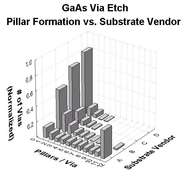
4 More recent work has focused on process development using chlorine-based chemistries in high density etch platforms such as inductively coupled plasma (ICP) and electron cyclotron resonance (ECR) reactors. While the ECR configuration is capable of higher plasma densities than an ICP, problems associated with scaling it to wafer sizes greater than 100 mm have precluded its widespread use as a high volume manufacturing solution. In this paper we characterize a manufacturable ICP-based high rate (10 μm/min) GaAs via etch process. This work is an extension of a production qualified 6 μm/min BCl 3 / Cl 2 etch process 16. In that work pillar-like features were observed in some fraction of the sample vias. Pillar formation was found to be a strong function of the substrate type (Figure 1). The present work was performed on the substrate type most prone to pillar formation (Vendor A) in an effort to develop a robust process that yields pillar-free etching independent of substrate type. Through the use of designed experiments, the GaAs etch rate, GaAs:photoresist etch selectivity and feature profile were explored as a function of process gas composition, ICP power, RF bias power and pressure. Experimental All wafers were etched on a Unaxis VLR 700 GaAs Via etcher. This commercially available tool uses a 2MHz RF inductively coupled coil to generate a high density plasma. Ion energy at the wafer surface is independently controlled by a MHz RF
5 bias applied to the cathode. Wafer temperature is maintained through the use of a fluid cooled cathode in conjunction with electrostatic clamping and He backside cooling. Plasma emission was monitored using a Unaxis Spectraworks optical emission spectrometer (OES). The spectral range was nm with a resolution of 1 nm using a 25 μm slit. The CCD detector was coupled to the sapphire reactor viewport with a silica optical fiber. The substrates etched in these experiments were 150 mm semi-insulating mechanical GaAs wafers patterned with a 14 μm thick photoresist mask. The total exposed area of the test pattern was approximately 15%. A large portion of the exposed area was due to a 3 mm photoresist edge bead removal process. Samples were exposed to plasma for 6 minutes unless otherwise noted. All GaAs etch depth measurements were taken using a step profilometer (Tencor P11). Initial and post-etch resist measurements were performed using a reflectance spectrometer (Nanospec 6100). Cross sections were analyzed by optical and scanning electron microscopy. Results and Discussion Plasma etch processes for GaAs typically utilize a chlorine based chemistry. As would be expected for a primarily chemically driven etch process, numerous studies have shown that the GaAs etch rate increases with increasing Cl concentration. In previous studies the Cl concentration has been increased by increasing pressure, increasing the percentage
6 Cl 2 in the feed gas composition, increasing total flow, or some combination of these factors. The dependence of GaAs etch rate on pressure has been widely reported particularly in the RIE configuration. Chen et. al 20 investigated the effect of higher process pressures (up to 50 mtorr) in an ECR configuration using an Ar / Cl 2 based process. The increased etch rate (6.7 μm/min) was at the expense of feature profile control with higher pressure processes resulting in isotropic etch profiles. Increasing the etch rate by increasing the Cl 2 fraction in the feed gas composition has also been widely reported. Shul et. al. 13 investigated ICP-based Ar / Cl 2 processes and found a maximum etch rate at a composition of 90% Cl 2. Constantine et. al. 14 investigated ICPbased BCl 3 / Cl 2 processes and found no etch rate increases for Cl 2 compositions greater than 75% Cl 2. Increasing the total flow of process gases has also been shown to increase GaAs etch rate at a fixed process pressure. The increased flow reduces the residence time of reactants, raising the concentration of available Cl while reducing the concentration of etch byproducts. Recent work has been reported for gas flows up to 200 sccm with a maximum etch rate of 10 μm/min 21. The present work explores the process space at ultra high gas flows (> 500 sccm) at relatively low operating pressures (< 25 mtorr) resulting in gas residence times on the
7 order of 0.1 seconds. Screening experiments over a range of process pressures and ICP powers confirm the relationship between process gas flow and GaAs etch rate (see Figure 2). During these screening experiments a maximum anisotropic etch rate of over 15.5 μm/min for a 100 micron diameter feature was observed. Based on the screening experiments, a designed experiment (DOE) was performed to map out the process space for high flows. While factorial experiments are a reliable way to map process responses, they quickly become cost prohibitive for a larger number of factors. Fractional factorial experiments are a convenient way to map factor responses, balancing time and material requirements with the quality of the calculated responses. A four factor half fractional (2 4-1 ) design was chosen to explore the process window. This design explores the process space of 4 factors in only 11 experiments (8 + 3 centerpoint repeats) but is unable to resolve two factor interactions. If a two factor interaction is indicated in the statistical analysis, further experiments would be required to isolate the interaction. No significant two factor interactions were indicated during the analysis of variance for these experiments. The designed experiment looked at four factors (pressure, ICP power, RF bias power, and feed gas composition). Figure 3 shows the range over which the factors were varied along with a schematic diagram of the half fractional design. During these experiments reactor temperatures, etch times, total process gas flow and hardware configuration were held constant. Note that total flow was held at a high (525 sccm) constant value based
8 on the results of the screening experiment. This flow / pressure combination resulted in a 0.13 second gas residence time for the centerpoint process. During the designed experiment, wafers with premeasured resist thicknesses were etched per the assigned recipe. Once etched, the wafers were inspected top down via optical microscope at 500x magnification to qualitatively assess the etched surface morphology. Following inspection, the final resist thickness was measured via reflectance spectrometer and the resist stripped. Following resist strip, the GaAs etch depth was measured by step profilometer. From these measurements, the GaAs etch rate, resist etch rate, and GaAs:photoresist etch selectivities were calculated. Feature profiles were evaluated by cross sectional SEM analysis. Figure 4 summarizes the DOE trends. During the analysis of the designed experiment the factor effects for each response were calculated and ranked using statistical software (Design Expert 6.0 Stat Ease Co). A half-normal plot was constructed in order to determine which factors reside above the noise floor and should be included in the model. Once the model factors were chosen, analysis of variance calculations were performed to determine if the model was adequate to map the response over the factor space. In the process space explored by the designed experiment, the GaAs removal rate increased solely with increasing ICP power (Figure 5). Previous designed experiments have shown GaAs etch rate to be a function of pressure, ICP power and feed gas
9 composition which is expected for a purely chemical etch mechanism. In these experiments, ICP power may be the sole factor affecting etch rate for two reasons: The GaAs etch rate may be limited by the fraction of the Cl 2 fed to the reactor which is dissociated into reactive Cl by the plasma. The degree of dissociation is expected to be dependent on the ICP power. The combination of high flows at low pressures yields short residence times (~ 0.1 seconds) which may result in a large excess of undissociated Cl 2. The DOE is limited to modeling the responses over the range of factors tested. Pressure and composition are still likely to affect the GaAs etch rate, just not significantly over the range of factors tested (9-15 mtorr & 80-90% Cl 2 ). It is important to note that due to metrology considerations, the DOE results are reported on 100 μm features. Due to the chemical nature of the GaAs via etch process, there is a large dependence of etch rate on feature aspect ratio 22,23. In an effort to quantify this relationship in the ultra-high flow regime, further validation experiments were performed using the centerpoint process. Figure 6 shows the relationship between feature size and etch rate. The argument to pursue faster GaAs etch rates is to decrease throughput time and ultimately cost of ownership. In order to realize these cost savings, etch rate alone is not sufficient. If the higher etch rate comes at the expense of poor etch rate uniformities, much of the time saved during the shorter main etch step is lost in the longer overetch times required to clear all features across the wafer. One of the benefits of etching in a
10 high flow, low pressure regime is the ability to achieve fast etch rates while maintaining excellent etch rate uniformity across the wafer. Figure 7 shows a uniformity map measured across a 53-point, regularly spaced array of 100 micron features with a 5 mm edge exclusion. For the 10 μm/min centerpoint process the GaAs etch rate uniformity was found to be ±2.8% (Range / 2 * Mean). The photoresist removal rate was found to be a strong function of RF bias power and ICP power and a weaker function of process pressure. The increase of resist etch rate with RF bias power and ICP power is consistent with a physical (sputtering) etch mechanism. Increasing RF bias increases the energy of ions bombarding the wafer surface while increasing ICP powers will increase the ion density, or flux, of ions bombarding the wafer surface. Both of these trends are consistent with a physical etch mechanism. The resist etch rate decreased with increasing pressure which is still consistent for a physical etch process the rate of a chemically driven process typically increases with increasing reactant concentration (pressure). The GaAs:Photoresist etch selectivity was determined by taking the ratio of the GaAs etch rates to the photoresist etch rates. GaAs:Photoresist etch selectivity was found to be solely a function of RF Bias power over the range of factors explored. Selectivity decreased with increasing RF Bias power. The etch selectivity can play a large role in the manufacturability of a via etch process particularly when a sloped via profile is required. Clayton et. al. 16 discussed the relationship between etch selectivity, initial photoresist profile and the final via profile. It is important to note that selectivity (and
11 potentially profile) is a function of RF Bias power while the GaAs rate is not. This allows the process to be adjusted over a wide range of via profiles, from vertical to highly sloped, independent of the GaAs etch rate. Immediately following etch (prior to resist strip) the wafers from the designed experiment were inspected optically for the presence of pillars in the vias. While most of the process conditions resulted in pillar free vias, a few design cells, particularly those at low ICP powers did exhibit some pillar formation. Attempts to model this response for the current design did not yield a model that could adequately map the response. In an effort to quantify this response, additional experiments using vendor A (those substrates most prone to pillar formation) substrates were performed. While no statistically significant response was obtained between pillar formation and the factors tested (RF bias power, ICP power, pressure, and composition), graphing observed pillar counts against the GaAs:photoresist etch selectivity (Figure 8) shows a clear qualitative trend. Pillar formation increases as the etch selectivity decreases. This relationship highlights the potential tradeoff between achieving sloped profiles while maintaining pillar-free vias particularly for vendor A substrates. This result contradicts the previous work of Nam et. al. 24 who found that pillar formation was reduced at higher RF bias powers. This apparent contradiction may be a result of the different process regimes explored in the two studies ( sccm total flow vs sccm total flow for current work).
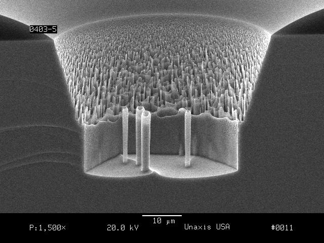
12 Following the analysis of the individual responses, a map of the process space was constructed (see Figure 9) constraining the GaAs etch rate to greater than 10 μm/min with a GaAs:Photoresist etch selectivity greater than 13:1 to ensure a sloped via using a sloped resist mask. Based on the preceding experiments, additional mechanical wafers were etched to validate process conditions aimed at providing a high rate (10 μm/min) via etch process with a sloped feature profile that minimized pillar formation. Figure 10 summarizes the etch results along with an optical cross section of a typical 40 μm diameter via. Conclusions In this article we report a high rate GaAs via etch process using a BCl 3 / Cl 2 based chemistry in a commercially available ICP reactor. GaAs etch rates in excess of 15 μm/min were reported for a near room temperature process using ultra high gas flows (greater than 500 sccm) at relatively low pressures (less than 20 mtorr). This process regime results in process gas residence times on the order of 0.1 seconds ensuring a high concentration of reactive Cl at the wafer surface. During the course of these experiments, pillar formation was observed in a limited number of design cells. Additional experiments showed that pillar formation increases as the GaAs:photoresist selectivity decreases. This relationship highlights the potential trade-off between eliminating pillar formation and the amount of slope achieved through erosion of a sloped photoresist mask
13 Through the use of designed experiments a production worthy GaAs-via etch process was characterized. This process is capable of fast etch rates ( μm diameter, μm diameter) over a wide range of GaAs:photoresist etch selectivities. Over the range of parameters explored, the RF Bias power allowed independent control of the GaAs:photoresist etch selectivity and ultimately via profile with the use of a sloped photoresist mask. Acknowledgments The authors would like to thank Fred Clayton, Motorola SPS, for the technical discussions as well as the substrate materials used in these experiments. References Cited 1. L.G. Hipwood, P.N. Wood, J. Vac. Sci. Technol. B 3, 395 (1985). 2. A.E. Geissberger, P.R. Claytor, J. Vac. Sci. Technol. A 3, 863 (1985). 3. R.J. Contolini, L.A. D Asaro, J. Vac. Sci. Technol. B 4, 706 (1986). 4. S. Salimian, C.B. Cooper, M.E. Day, J. Vac. Sci. Technol. B 4, 1606 (1987). 5. A. Camacho, D.V. Morgan, J. Vac. Sci. Technol. B 12, 2933 (1994). 6. H. Takano, K. Sumitani, H. Matsuoka, K. Sato, O. Ishihara, N. Tsubouchi, J. Vac. Sci. Technol. B 14, 112 (1996). 7. A. Mitra, C.D. Nordquist, T.N. Jackson, T.S. Mayer, J. Vac. Sci. Technol. B 16, 2695 (1998).
14 8. R. Shul, M.L. Lovejoy, J.C. Word, A.J. Howard, D.J. Rieger, S.H. Dravitz, J. Vac. Sci. Technol. B 15, 657 (1997). 9. M.S. Chung, H.R. Kim, J.E. Lee, B.K. Kang, B.M. Kim, J. Vac. Sci. Technol. B 11, 159 (1993). 10. K.J. Nordheden, D.W. Ferguson, P.M. Smith, J. Vac. Sci. Technol. B 11, 1879 (1993). 11. J. Lee, H. Tsai, Y.S. Chang, R.T. Huang, GaAs MANTECH Proc. 71 (2000). 12. D.E. Ibbotson, D.L. Flamm, V.M. Donnelly, J. Appl. Phys. 54, 5974 (1983). 13. R.J. Shul, G.B. McClellan, R.D. Briggs, D.J. Rieger, S.J. Pearton, C.R. Abernathy, J.W. Lee, C. Constantine, C. Barratt, J. Vac. Sci. Technol. A 15, 633 (1996). 14. C. Constantine, D. Johnson, C. Barratt, R.J. Shul, G.B. McClellan, R.D. Briggs, D.J. Rieger, R.F. Karlicek, J.W. Lee, S.J. Pearton, Mater. Res. Soc. Symp. Proc. 421, 431 (1996). 15. E.W. Berg, S.W. Pang, J. Electrochem. Soc. 146, 775 (1999). 16. F. Clayton, R. Westerman, D. Johnson, GaAs MANTECH Proc. 121 (2002). 17. F. Ren, S.J. Pearton, C.R. Abernathy, R. Esagui, T.R. Fullowan, P.W. Wisk, J.R. Lothian, Semicond. Sci. Technol. 7, 850 (1992). 18. S.W. Pang, K.K. Ko, J. Vac. Sci. Technol. B 10, 2703 (1992). 19. S.J. Pearton, F. Ren, A. Katz, J.R. Lothian, T.R. Fullowan, B Tseng, J. Vac. Sci. Technol. B 11, 152 (1993). 20. Y.W. Chen, B.S. Ooi, G.I. Ng, K. Radhakrishnan, C.L. Tan, J. Vac. Sci. Technol. B 18, 2509 (2000). 21. D. Bonneau, P. Borkowski, R. Shelley, A. Fortier, M.C. Young, C. Fragos, S. Anderson, GaAs MANTECH Proc. 113, (2002).
15 22. B. Abraham-Shrauner, J. Vac. Sci. Technol. B 17, 158 (1999). 23. B. Abraham-Shrauner, K.J. Nordheden, Y.S. Lee, J. Vac. Sci. Technol. B 17, 961 (1999). 24. P.S. Nam, L.M. Ferreira, T.Y. Lee, K.N. Tu, J. Vac. Sci. Technol. B 18, 2780 (2000).
16 Figure Captions Figure 1. Pillar formation as a function of substrate supplier. Material D shows 80% pillar free vias on thinned and mounted 150mm GaAs slices. Material A shows 10% pillar free vias for the same process conditions. 16 Figure 2. Effect of Cl 2 flow rate on GaAs etch rate. Graph summarizes a number of screening experiments performed over a range of pressures, feed gas compositions and ICP powers. Figure 3. Summary of designed experiment. Range of factors explored and schematic of design. Black nodes on design schematic indicate experimental conditions. Figure 4. Response trends from designed experiment. Figure 5. Analyzed GaAs etch rate response from designed experiment. A. Half normal plot showing ICP power as the only significant factor affecting GaAs etch rate over the range of parameters tested. B. Factor effect plot showing GaAs etch rate as a function ICP power. Figure 6. GaAs etch rate as a function of feature width. Etch rates determined from multiple cross sections of a single wafer etched at the DOE centerpoint process for 6 minutes. Multiple sizes of vias and trenches were sampled.
17 Figure 7. GaAs etch depth uniformity from the DOE center point process. The uniformity map was constructed from a 53-point regularly spaced array using a 5 mm edge exclusion. The wafer was etched for 6 minutes. Figure 8. Pillar count as a function of GaAs:photoresist etch selectivity (substrate vendor A material). Note the potential trade-off between pillar formation and final via etch profile. Figure 9. Process space as a function of ICP power and RF bias power. Figure 10. Summary of process capability for optimized GaAs via etch process. Inset micrograph shows optical cross section of 40 μm diameter via note slope induced by erosion of sloped photoresist mask.
18 Figure 1.
19 20 GaAs Etch Rate vs. Cl 2 Flow 100 μm Diameter Via 16 GaAs Etch Rate (μm/min) Cl 2 Flow (sccm) Figure 2
20 Design Layout Factor Name Low High Pressure mtorr 9 15 ICP W RIE W % Cl 2 % Constants Total Flow Etch Time Temperature 525 sccm 5 min 15 C RIE Composition ICP RIE Composition ICP Hardware GaAs Via III Pressure Low Pressure High Figure 3
21 Response Response GaAs Rate Resist Rate GaAs:Resist Selectivity DC Bias Pressure Factor ICP RF Bias % Cl 2 Figure 4
22 A. Half Normal plot B. Effect plot Half Normal % probability ICP GaAs Rate Effect ICP Figure 5
 120 Figure 6")
23 GaAs Etch Rate vs Feature Size Etch Rate (um/min) Feature Width (um) 120 Figure 6

24 Wafer GaAs Via III Mean 64.5 um Uf 2.8% Rng Figure 7

25 Pillar Count vs GaAs:PR Selectivity GaAs Via Etch Pillar Count GaAs:PR Etch Selectivity Figure 8
26 Select > 13:1 DESIGN-EXPERT Plot Overlay Plot X = RF Bias Y = ICP Power Overlay Plot Actual Factors Pressure = 12 mtorr %Cl 2 = 85 % ICP GaAs Rate> 10 um/min Figure 9 RF Bias

27 GaAs Via III - Process Performance GaAs Etch Rate 8.3 um/min 40 um via 10.1 um/min 100 um via GaAs:PR Selectivity 15 : 1 Via Profile Sloped * GaAs Rate Uniformity < 5% Morphology Specular Optical cross-section of 40 um diameter via * using sloped PR mask Figure 10.
Cl 2 -Based Dry Etching of GaN and InGaN Using Inductively Coupled Plasma
 Journal of The Electrochemical Society, 147 (5) 1859-1863 (2000) 1859 Cl 2 -Based Dry Etching of GaN and InGaN Using Inductively Coupled Plasma The Effects of Gas Additives Ji-Myon Lee, Ki-Myung Chang,
ETCHING Chapter 10. Mask. Photoresist
 ETCHING Chapter 10 Mask Light Deposited Substrate Photoresist Etch mask deposition Photoresist application Exposure Development Etching Resist removal Etching of thin films and sometimes the silicon substrate
Etching Capabilities at Harvard CNS. March 2008
 Etching Capabilities at Harvard CNS March 2008 CNS: A shared use facility for the Harvard Community and New England CNS Provides technical support, equipment and staff. Explicitly multi-disciplinary w/
Advances in Back-side Via Etching of SiC for GaN Device Applications
 Advances in Back-side Via Etching of SiC for GaN Device Applications Anthony Barker, Kevin Riddell, Huma Ashraf & Dave Thomas SPTS Technologies, Ringland Way, Newport NP18 2TA, UK, dave.thomas@spts.com,
Reactive Ion Etching (RIE)
") Reactive Ion Etching (RIE) RF 13.56 ~ MHz plasma Parallel-Plate Reactor wafers Sputtering Plasma generates (1) Ions (2) Activated neutrals Enhance chemical reaction 1 2 Remote Plasma Reactors Plasma Sources
Reactive Ion Etching (RIE) RF 13.56 ~ MHz plasma Parallel-Plate Reactor wafers Sputtering Plasma generates (1) Ions (2) Activated neutrals Enhance chemical reaction 1 2 Remote Plasma Reactors Plasma Sources
Etching: Basic Terminology
 Lecture 7 Etching Etching: Basic Terminology Introduction : Etching of thin films and sometimes the silicon substrate are very common process steps. Usually selectivity, and directionality are the first
Etching Issues - Anisotropy. Dry Etching. Dry Etching Overview. Etching Issues - Selectivity
 Etching Issues - Anisotropy Dry Etching Dr. Bruce K. Gale Fundamentals of Micromachining BIOEN 6421 EL EN 5221 and 6221 ME EN 5960 and 6960 Isotropic etchants etch at the same rate in every direction mask
E SC 412 Nanotechnology: Materials, Infrastructure, and Safety Wook Jun Nam
 E SC 412 Nanotechnology: Materials, Infrastructure, and Safety Wook Jun Nam Lecture 10 Outline 1. Wet Etching/Vapor Phase Etching 2. Dry Etching DC/RF Plasma Plasma Reactors Materials/Gases Etching Parameters
Section 3: Etching. Jaeger Chapter 2 Reader
 Section 3: Etching Jaeger Chapter 2 Reader Etch rate Etch Process - Figures of Merit Etch rate uniformity Selectivity Anisotropy d m Bias and anisotropy etching mask h f substrate d f d m substrate d f
Plasma etching. Bibliography
 Plasma etching Bibliography 1. B. Chapman, Glow discharge processes, (Wiley, New York, 1980). - Classical plasma processing of etching and sputtering 2. D. M. Manos and D. L. Flamm, Plasma etching; An
Defense Technical Information Center Compilation Part Notice
 UNCLASSIFIED Defense Technical Information Center Compilation Part Notice ADP013351 TITLE: The Effects of Plasma Induced Damage on the Channel Layers of Ion Implanted GaAs MESFETs during Reactive Ion Etching
Wet and Dry Etching. Theory
 Wet and Dry Etching Theory 1. Introduction Etching techniques are commonly used in the fabrication processes of semiconductor devices to remove selected layers for the purposes of pattern transfer, wafer
Inductively Coupled Plasma Etching of Ta, Co, Fe, NiFe, NiFeCo, and MnNi with Cl 2 /Ar Discharges
 Korean J. Chem. Eng., 21(6), 1235-1239 (2004) Inductively Coupled Plasma Etching of Ta, Co, Fe, NiFe, NiFeCo, and MnNi with Cl 2 /Ar Discharges Hyung Jo Park*, Hyun-Wook Ra, Kwang Sup Song** and Yoon-Bong
LECTURE 5 SUMMARY OF KEY IDEAS
 LECTURE 5 SUMMARY OF KEY IDEAS Etching is a processing step following lithography: it transfers a circuit image from the photoresist to materials form which devices are made or to hard masking or sacrificial
MODELING OF SEASONING OF REACTORS: EFFECTS OF ION ENERGY DISTRIBUTIONS TO CHAMBER WALLS*
 MODELING OF SEASONING OF REACTORS: EFFECTS OF ION ENERGY DISTRIBUTIONS TO CHAMBER WALLS* Ankur Agarwal a) and Mark J. Kushner b) a) Department of Chemical and Biomolecular Engineering University of Illinois,
INTRODUCTION TO THE HYBRID PLASMA EQUIPMENT MODEL
 INTRODUCTION TO THE HYBRID PLASMA EQUIPMENT MODEL Prof. Mark J. Kushner Department of Electrical and Computer Engineering 1406 W. Green St. Urbana, IL 61801 217-144-5137 mjk@uiuc.edu http://uigelz.ece.uiuc.edu
Sensors and Metrology. Outline
 Sensors and Metrology A Survey 1 Outline General Issues & the SIA Roadmap Post-Process Sensing (SEM/AFM, placement) In-Process (or potential in-process) Sensors temperature (pyrometry, thermocouples, acoustic
Chapter 7. Plasma Basics
 Chapter 7 Plasma Basics 2006/4/12 1 Objectives List at least three IC processes using plasma Name three important collisions in plasma Describe mean free path Explain how plasma enhance etch and CVD processes
UNIVERSITY OF CALIFORNIA College of Engineering Department of Electrical Engineering and Computer Sciences. Fall Exam 1
 UNIVERSITY OF CALIFORNIA College of Engineering Department of Electrical Engineering and Computer Sciences EECS 143 Fall 2008 Exam 1 Professor Ali Javey Answer Key Name: SID: 1337 Closed book. One sheet
The Stanford Nanofabrication Facility. Etch Area Overview. May 21, 2013
 The Stanford Nanofabrication Facility Etch Area Overview May 21, 2013 High Density Plasma Systems Etcher Materials Etched Gases available Wafer Size Applied Materials P5000 MRIE ChA Applied Materials P5000
Chapter 7 Plasma Basic
 Chapter 7 Plasma Basic Hong Xiao, Ph. D. hxiao89@hotmail.com www2.austin.cc.tx.us/hongxiao/book.htm Hong Xiao, Ph. D. www2.austin.cc.tx.us/hongxiao/book.htm 1 Objectives List at least three IC processes
Plasma Chemistry Study in an Inductively Coupled Dielectric Etcher
 Plasma Chemistry Study in an Inductively Coupled Dielectric Etcher Chunshi Cui, John Trow, Ken Collins, Betty Tang, Luke Zhang, Steve Shannon, and Yan Ye Applied Materials, Inc. October 26, 2000 10/28/2008
SUPPLEMENTARY NOTES Supplementary Note 1: Fabrication of Scanning Thermal Microscopy Probes
 SUPPLEMENTARY NOTES Supplementary Note 1: Fabrication of Scanning Thermal Microscopy Probes Fabrication of the scanning thermal microscopy (SThM) probes is summarized in Supplementary Fig. 1 and proceeds
Inductively Coupled Plasma Reactive Ion Etching of GeSbTe Thin Films in a HBr/Ar Gas
 Integrated Ferroelectrics, 90: 95 106, 2007 Copyright Taylor & Francis Group, LLC ISSN 1058-4587 print / 1607-8489 online DOI: 10.1080/10584580701249371 Inductively Coupled Plasma Reactive Ion Etching
UHF-ECR Plasma Etching System for Dielectric Films of Next-generation Semiconductor Devices
 UHF-ECR Plasma Etching System for Dielectric Films of Next-generation Semiconductor Devices 1 UHF-ECR Plasma Etching System for Dielectric Films of Next-generation Semiconductor Devices Katsuya Watanabe
Supplementary Figure 1 Detailed illustration on the fabrication process of templatestripped
 Supplementary Figure 1 Detailed illustration on the fabrication process of templatestripped gold substrate. (a) Spin coating of hydrogen silsesquioxane (HSQ) resist onto the silicon substrate with a thickness
The Gaseous Electronic Conference GEC reference cell as a benchmark for understanding microelectronics processing plasmas*
 PHYSICS OF PLASMAS VOLUME 6, NUMBER 5 MAY 1999 The Gaseous Electronic Conference GEC reference cell as a benchmark for understanding microelectronics processing plasmas* M. L. Brake, J. Pender, a) and
Characteristics of Neutral Beam Generated by a Low Angle Reflection and Its Etch Characteristics by Halogen-Based Gases
 Characteristics of Neutral Beam Generated by a Low Angle Reflection and Its Etch Characteristics by Halogen-Based Gases Geun-Young Yeom SungKyunKwan University Problems of Current Etch Technology Scaling
University of California, Santa Barbara Santa Barbara, California 93106
 HIGH-ASPECT-RATIO INDUCTIVELY COUPLED PLASMA ETCHING OF BULK TITANIUM FOR MEMS APPLICATIONS E. R. Parker 1, M. F. Aimi 2, B. J. Thibeault 3, M. P. Rao 1, and N. C. MacDonald 1,2 1 Mechanical and Environmental
Three Approaches for Nanopatterning
 Three Approaches for Nanopatterning Lithography allows the design of arbitrary pattern geometry but maybe high cost and low throughput Self-Assembly offers high throughput and low cost but limited selections
Lecture 15 Etching. Chapters 15 & 16 Wolf and Tauber. ECE611 / CHE611 Electronic Materials Processing Fall John Labram 1/76
 Lecture 15 Etching Chapters 15 & 16 Wolf and Tauber 1/76 Announcements Term Paper: You are expected to produce a 4-5 page term paper on a selected topic (from a list). Term paper contributes 25% of course
MICROCHIP MANUFACTURING by S. Wolf
 by S. Wolf Chapter 15 ALUMINUM THIN-FILMS and SPUTTER-DEPOSITION 2004 by LATTICE PRESS CHAPTER 15 - CONTENTS Aluminum Thin-Films Sputter-Deposition Process Steps Physics of Sputter-Deposition Magnetron-Sputtering
In-Situ Measurement of the Relative Thermal Contributions of Chemical Reactions and Ions During Plasma Etching. M.R. Tesauro a, and G.
 10.1149/1.3035362 The Electrochemical Society In-Situ Measurement of the Relative Thermal Contributions of Chemical Reactions and Ions During Plasma Etching M.R. Tesauro a, and G. Roche b a Qimonda Dresden
Manufacturable AlGaAs/GaAs HBT Implant Isolation Process Using Doubly Charged Helium
 Manufacturable AlGaAs/GaAs HBT Implant Isolation Process Using Doubly Charged Helium ABSTRACT Rainier Lee, Shiban Tiku, and Wanming Sun Conexant Systems 2427 W. Hillcrest Drive Newbury Park, CA 91320 (805)
Plasma Etch Tool Gap Distance DOE Final Report
 Plasma Etch Tool Gap Distance DOE Final Report IEE 572 Doug Purvis Mei Lee Gallagher 12/4/00 Page 1 of 10 Protocol Purpose: To establish new Power, Pressure, and Gas Ratio setpoints that are acceptable
Normally-Off GaN Field Effect Power Transistors: Device Design and Process Technology Development
 Center for High Performance Power Electronics Normally-Off GaN Field Effect Power Transistors: Device Design and Process Technology Development Dr. Wu Lu (614-292-3462, lu.173@osu.edu) Dr. Siddharth Rajan
CHAPTER 6: Etching. Chapter 6 1
 Chapter 6 1 CHAPTER 6: Etching Different etching processes are selected depending upon the particular material to be removed. As shown in Figure 6.1, wet chemical processes result in isotropic etching
Nanopantography: A method for parallel writing of etched and deposited nanopatterns
 Nanopantography: A method for parallel writing of etched and deposited nanopatterns Vincent M. Donnelly 1, Lin Xu 1, Azeem Nasrullah 2, Zhiying Chen 1, Sri C. Vemula 2, Manish Jain 1, Demetre J. Economou
H. Shin, W. Zhu, V. M. Donnelly, and D. J. Economou University of Houston. November 2, AVS 58h International Symposium, Nashville, TN, USA
 Near-Threshold Ion-Enhanced Silicon Etching H. Shin, W. Zhu, V. M. Donnelly, and D. J. Economou o ou University of Houston Acknowledgements: DOE Plasma Science Center, NSF and Varian Semiconductor Equipment
Analyses of LiNbO 3 wafer surface etched by ECR plasma of CHF 3 & CF 4
 1998 DRY PROCESS SYMPOSIUM VI - 3 Analyses of LiNbO 3 wafer surface etched by ECR plasma of CHF 3 & CF 4 Naoki Mitsugi, Kaori Shima, Masumi Ishizuka and Hirotoshi Nagata New Technology Research Laboratories,
Dry Etching Zheng Yang ERF 3017, MW 5:15-6:00 pm
 Dry Etching Zheng Yang ERF 3017, email: yangzhen@uic.edu, MW 5:15-6:00 pm Page 1 Page 2 Dry Etching Why dry etching? - WE is limited to pattern sizes above 3mm - WE is isotropic causing underetching -
Optical Measurements of Critical Dimensions at Several Stages of the Mask Fabrication Process
 Optical Measurements of Critical Dimensions at Several Stages of the Mask Fabrication Process John C. Lam, Alexander Gray n&k Technology, Inc., Santa Clara, CA ABSTRACT Critical dimension (CD) metrology
UNIT 3. By: Ajay Kumar Gautam Asst. Prof. Dev Bhoomi Institute of Technology & Engineering, Dehradun
 UNIT 3 By: Ajay Kumar Gautam Asst. Prof. Dev Bhoomi Institute of Technology & Engineering, Dehradun 1 Syllabus Lithography: photolithography and pattern transfer, Optical and non optical lithography, electron,
4FNJDPOEVDUPS 'BCSJDBUJPO &UDI
 2010.5.4 1 Major Fabrication Steps in CMOS Process Flow UV light oxygen Silicon dioxide Silicon substrate Oxidation (Field oxide) photoresist Photoresist Coating Mask exposed photoresist Mask-Wafer Exposed
Gas utilization in remote plasma cleaning and stripping applications
 Gas utilization in remote plasma cleaning and stripping applications B. E. E. Kastenmeier IBM Semiconductor Research and Development Center, 2070 Rt. 52, Zip E40, Hopewell Junction, New York 12533 G. S.
Characterization of Optical Proximity Correction Features
 Characterization of Optical Proximity Correction Features John Allgair, Michelle Ivy, Kevin Lucas, John Sturtevant Motorola APRDL, Austin, TX 7871 Richard Elliott, Chris A. Mack, Craig MacNaughton, John
Nanostructures Fabrication Methods
 Nanostructures Fabrication Methods bottom-up methods ( atom by atom ) In the bottom-up approach, atoms, molecules and even nanoparticles themselves can be used as the building blocks for the creation of
Supplementary Information Our InGaN/GaN multiple quantum wells (MQWs) based one-dimensional (1D) grating structures
 based one-dimensional (1D) grating structures") Polarized white light from hybrid organic/iii-nitrides grating structures M. Athanasiou, R. M. Smith, S. Ghataora and T. Wang* Department of Electronic and Electrical Engineering, University of Sheffield,
Polarized white light from hybrid organic/iii-nitrides grating structures M. Athanasiou, R. M. Smith, S. Ghataora and T. Wang* Department of Electronic and Electrical Engineering, University of Sheffield,
Chapter 2 FABRICATION PROCEDURE AND TESTING SETUP. Our group has been working on the III-V epitaxy light emitting materials which could be
 Chapter 2 7 FABRICATION PROCEDURE AND TESTING SETUP 2.1 Introduction In this chapter, the fabrication procedures and the testing setups for the sub-micrometer lasers, the submicron disk laser and the photonic
SUPPLEMENTARY INFORMATION
 In the format provided by the authors and unedited. DOI: 10.1038/NPHOTON.2016.254 Measurement of non-monotonic Casimir forces between silicon nanostructures Supplementary information L. Tang 1, M. Wang
EE 527 MICROFABRICATION. Lecture 25 Tai-Chang Chen University of Washington
 EE 527 MICROFABRICATION Lecture 25 Tai-Chang Chen University of Washington ION MILLING SYSTEM Kaufmann source Use e-beam to strike plasma A magnetic field applied to increase ion density Drawback Low etch
Wafer Charging in Process Equipment and its Relationship to GMR Heads Charging Damage
 Wafer Charging in Process Equipment and its Relationship to GMR Heads Charging Damage Wes Lukaszek Wafer Charging Monitors, Inc. 127 Marine Road, Woodside, CA 94062 tel.: (650) 851-9313, fax.: (650) 851-2252,
Plasma Etching: Atomic Scale Surface Fidelity and 2D Materials
 1 Plasma Etching: Atomic Scale Surface Fidelity and 2D Materials Thorsten Lill, Keren J. Kanarik, Samantha Tan, Meihua Shen, Alex Yoon, Eric Hudson, Yang Pan, Jeffrey Marks, Vahid Vahedi, Richard A. Gottscho
Improvement of MgO Characteristics Using RF-Plasma Treatment in AC Plasma Display Panel
 Mol. Cryst. Liq. Cryst., Vol. 531: pp. 73=[373] 81=[381], 2010 Copyright # Taylor & Francis Group, LLC ISSN: 1542-1406 print=1563-5287 online DOI: 10.1080/15421406.2010.499331 Improvement of MgO Characteristics
Fast Non-destructive Optical Measurements of Critical Dimension Uniformity and Linearity on AEI and ASI Phase-shift Masks
 Fast Non-destructive Optical Measurements of Critical Dimension Uniformity and Linearity on AI and ASI Phase-shift Masks Alexander Gray University of California at Davis, CA John C. Lam n&k Technology,
Feature Profile Evolution during Shallow Trench Isolation (STI) Etch in Chlorine-based Plasmas
 Etch in Chlorine-based Plasmas") 1 Feature Profile Evolution during Shallow Trench Isolation (STI) Etch in Chlorine-based Plasmas Presentation November 14, 2005 Jane P. Chang and John Hoang Department of Chemical and Biomolecular Engineering
1 Feature Profile Evolution during Shallow Trench Isolation (STI) Etch in Chlorine-based Plasmas Presentation November 14, 2005 Jane P. Chang and John Hoang Department of Chemical and Biomolecular Engineering
Regents of the University of California
 Deep Reactive-Ion Etching (DRIE) DRIE Issues: Etch Rate Variance The Bosch process: Inductively-coupled plasma Etch Rate: 1.5-4 μm/min Two main cycles in the etch: Etch cycle (5-15 s): SF 6 (SF x+ ) etches
Lecture 6 Plasmas. Chapters 10 &16 Wolf and Tauber. ECE611 / CHE611 Electronic Materials Processing Fall John Labram 1/68
 Lecture 6 Plasmas Chapters 10 &16 Wolf and Tauber 1/68 Announcements Homework: Homework will be returned to you on Thursday (12 th October). Solutions will be also posted online on Thursday (12 th October)
PARTICLE CONTROL AT 100 nm NODE STATUS WORKSHOP: PARTICLES IN PLASMAS
 PARTICLE CONTROL AT 100 nm NODE STATUS WORKSHOP: PARTICLES IN PLASMAS Mark J. Kushner University of Illinois Department of Electrical and Computer Engineering Urbana, IL 61801 mjk@uiuc.edu December 1998
After Development Inspection (ADI) Studies of Photo Resist Defectivity of an Advanced Memory Device
 Studies of Photo Resist Defectivity of an Advanced Memory Device") After Development Inspection (ADI) Studies of Photo Resist Defectivity of an Advanced Memory Device Hyung-Seop Kim, Yong Min Cho, Byoung-Ho Lee Semiconductor R&D Center, Device Solution Business, Samsung
After Development Inspection (ADI) Studies of Photo Resist Defectivity of an Advanced Memory Device Hyung-Seop Kim, Yong Min Cho, Byoung-Ho Lee Semiconductor R&D Center, Device Solution Business, Samsung
DOE WEB SEMINAR,
 DOE WEB SEMINAR, 2013.03.29 Electron energy distribution function of the plasma in the presence of both capacitive field and inductive field : from electron heating to plasma processing control 1 mm PR
NNCI ETCH WORKSHOP - STANFORD NNCI PLASMA ETCH OVERVIEW. Usha Raghuram Stanford Nanofabrication Facility Stanford, CA May 24, 2016
 NNCI ETCH WORKSHOP - STANFORD NNCI PLASMA ETCH OVERVIEW Usha Raghuram Stanford Nanofabrication Facility Stanford, CA May 24, 2016 NNCI AT STANFORD Four labs under NNCI Umbrella at Stanford SNSF Stanford
Defining quality standards for the analysis of solid samples
 Defining quality standards for the analysis of solid samples Thermo Scientific Element GD Plus Glow Discharge Mass Spectrometer Redefine your quality standards for the elemental analysis of solid samples
Continuous room-temperature operation of optically pumped InGaAs/InGaAsP microdisk lasers
 Continuous room-temperature operation of optically pumped InGaAs/InGaAsP microdisk lasers S. M. K. Thiyagarajan, A. F. J. Levi, C. K. Lin, I. Kim, P. D. Dapkus, and S. J. Pearton + Department of Electrical
Lecture 11. Etching Techniques Reading: Chapter 11. ECE Dr. Alan Doolittle
 Lecture 11 Etching Techniques Reading: Chapter 11 Etching Techniques Characterized by: 1.) Etch rate (A/minute) 2.) Selectivity: S=etch rate material 1 / etch rate material 2 is said to have a selectivity
Effects of plasma treatment on the precipitation of fluorine-doped silicon oxide
 ARTICLE IN PRESS Journal of Physics and Chemistry of Solids 69 (2008) 555 560 www.elsevier.com/locate/jpcs Effects of plasma treatment on the precipitation of fluorine-doped silicon oxide Jun Wu a,, Ying-Lang
Application of the GD-Profiler 2 to the PV domain
 Application of the GD-Profiler 2 to the PV domain GD Profiler 2 RF GDOES permits to follow the distribution of the elements as function of depth. This is an ultra fast characterisation technique capable
Effect of Spiral Microwave Antenna Configuration on the Production of Nano-crystalline Film by Chemical Sputtering in ECR Plasma
 THE HARRIS SCIENCE REVIEW OF DOSHISHA UNIVERSITY, VOL. 56, No. 1 April 2015 Effect of Spiral Microwave Antenna Configuration on the Production of Nano-crystalline Film by Chemical Sputtering in ECR Plasma
Fabrication of Sub-Quarter-Micron Grating Patterns by Employing Lithography
 MCROU,!~'O~C ELSEVER Microelectronic Engineering 46 (1999) 173-177 Fabrication of Sub-Quarter-Micron Grating Patterns by Employing Lithography DUV Holographic L. A. Wang*, C. H. Lin and J. H. Chen nstitute
ELEC 7364 Lecture Notes Summer Etching. by STELLA W. PANG. from The University of Michigan, Ann Arbor, MI, USA
 ELEC 7364 Lecture Notes Summer 2008 Etching by STELLA W. PANG from The University of Michigan, Ann Arbor, MI, USA Visiting Professor at The University of Hong Kong The University of Michigan on Visiting
Exploration into Sputtered ITO Film Properties as a Function of Magnetic Field Strength
 Tangential Magnetic Flux, Gauss Exploration into Sputtered ITO Film Properties as a Function of Magnetic Field Strength Patrick Morse and Timmy Strait Sputtering Components Inc. Owatonna Minnesota ABSTRACT
The effect of the chamber wall on fluorocarbonassisted atomic layer etching of SiO 2 using cyclic Ar/C 4 F 8 plasma
 The effect of the chamber wall on fluorocarbonassisted atomic layer etching of SiO 2 using cyclic Ar/C 4 F 8 plasma Running title: The effect of the chamber wall on FC assisted atomic layer etching of
Interhalogen plasma chemistries for dry etch patterning of Ni, Fe, NiFe and NiFeCo thin films
 Ž. Applied Surface Science 140 1999 215 222 Interhalogen plasma chemistries for dry etch patterning of Ni, Fe, NiFe and NiFeCo thin films H. Cho a,), K.B. Jung a, D.C. Hays a, Y.B. Hahn a,1, E.S. Lambers
EE 143 MICROFABRICATION TECHNOLOGY FALL 2014 C. Nguyen PROBLEM SET #7. Due: Friday, Oct. 24, 2014, 8:00 a.m. in the EE 143 homework box near 140 Cory
 Issued: Tuesday, Oct. 14, 2014 PROBLEM SET #7 Due: Friday, Oct. 24, 2014, 8:00 a.m. in the EE 143 homework box near 140 Cory Electroplating 1. Suppose you want to fabricate MEMS clamped-clamped beam structures
Dynamization evolution of Dry Etch Tools in Semiconductor Device Fabrication Gordon Cameron Intel Corp (November 2005)
") Dynamization evolution of Dry Etch Tools in Semiconductor Device Fabrication Gordon Cameron Intel Corp (November 2005) Abstract Engineering Systems follow recognized trends of evolution; the main parameters
Dynamization evolution of Dry Etch Tools in Semiconductor Device Fabrication Gordon Cameron Intel Corp (November 2005) Abstract Engineering Systems follow recognized trends of evolution; the main parameters
Plasma atomic layer etching using conventional plasma equipment
 Plasma atomic layer etching using conventional plasma equipment Ankur Agarwal a Department of Chemical and Biomolecular Engineering, University of Illinois, 600 S. Mathews Ave., Urbana, Illinois 61801
Effect of Noble Gas. Plasma Processing Laboratory University of Houston. Acknowledgements: DoE Plasma Science Center and NSF
 Ion Energy Distributions in Pulsed Plasmas with Synchronous DC Bias: Effect of Noble Gas W. Zhu, H. Shin, V. M. Donnelly and D. J. Economou Plasma Processing Laboratory University of Houston Acknowledgements:
Thin Wafer Handling Challenges and Emerging Solutions
 1 Thin Wafer Handling Challenges and Emerging Solutions Dr. Shari Farrens, Mr. Pete Bisson, Mr. Sumant Sood and Mr. James Hermanowski SUSS MicroTec, 228 Suss Drive, Waterbury Center, VT 05655, USA 2 Thin
Device Fabrication: Etch
 Device Fabrication: Etch 1 Objectives Upon finishing this course, you should able to: Familiar with etch terminology Compare wet and dry etch processes processing and list the main dry etch etchants Become
Mater. Res. Soc. Symp. Proc. Vol Materials Research Society
 Mater. Res. Soc. Symp. Proc. Vol. 1258 2010 Materials Research Society 1258-Q14-02 Realization of silicon nanopillar arrays with controllable sidewall profiles by holography lithography and a novel single-step
Focused-ion-beam milling based nanostencil mask fabrication for spin transfer torque studies. Güntherodt
 Focused-ion-beam milling based nanostencil mask fabrication for spin transfer torque studies B. Özyilmaz a, G. Richter, N. Müsgens, M. Fraune, M. Hawraneck, B. Beschoten b, and G. Güntherodt Physikalisches
CHARACTERIZATION OF DEEP REACTIVE ION ETCHING (DRIE) PROCESS FOR ELECTRICAL THROUGH-WAFER INTERCONNECTS FOR PIEZORESISTIVE INERTIAL SENSORS
 PROCESS FOR ELECTRICAL THROUGH-WAFER INTERCONNECTS FOR PIEZORESISTIVE INERTIAL SENSORS") CHARACTERIZATION OF DEEP REACTIVE ION ETCHING (DRIE) PROCESS FOR ELECTRICAL THROUGH-WAFER INTERCONNECTS FOR PIEZORESISTIVE INERTIAL SENSORS Maria Suggs, Physics Major, Southern Polytechnic State University
CHARACTERIZATION OF DEEP REACTIVE ION ETCHING (DRIE) PROCESS FOR ELECTRICAL THROUGH-WAFER INTERCONNECTS FOR PIEZORESISTIVE INERTIAL SENSORS Maria Suggs, Physics Major, Southern Polytechnic State University
P. Diomede, D. J. Economou and V. M. Donnelly Plasma Processing Laboratory, University of Houston
 P. Diomede, D. J. Economou and V. M. Donnelly Plasma Processing Laboratory, University of Houston 1 Outline Introduction PIC-MCC simulation of tailored bias on boundary electrode Semi-analytic model Comparison
Fabrication and Domain Imaging of Iron Magnetic Nanowire Arrays
 Abstract #: 983 Program # MI+NS+TuA9 Fabrication and Domain Imaging of Iron Magnetic Nanowire Arrays D. A. Tulchinsky, M. H. Kelley, J. J. McClelland, R. Gupta, R. J. Celotta National Institute of Standards
Si etching in high-density SF 6 plasmas for microfabrication: surface roughness formation
 Microelectronic Engineering 73 74 (2004) 312 318 www.elsevier.com/locate/mee Si etching in high-density SF 6 plasmas for microfabrication: surface roughness formation E. Gogolides *, C. Boukouras, G. Kokkoris,
In situ electrical characterization of dielectric thin films directly exposed to plasma vacuum-ultraviolet radiation
 JOURNAL OF APPLIED PHYSICS VOLUME 88, NUMBER 4 15 AUGUST 2000 In situ electrical characterization of dielectric thin films directly exposed to plasma vacuum-ultraviolet radiation C. Cismaru a) and J. L.
M. Audronis 1 and F. Zimone 2 1. Nova Fabrica Ltd. 1. Angstrom Sciences Inc.
 M. Audronis 1 and F. Zimone 2 1 Nova Fabrica Ltd. 1 Angstrom Sciences Inc. Email: info@novafabrica.biz 1 Founded in 2013 the company is based in Lithuania (northern EU). NF are involved in two business
Sensors and Metrology
 Sensors and Metrology A Survey 1 Outline General Issues & the SIA Roadmap Post-Process Sensing (SEM/AFM, placement) In-Process (or potential in-process) Sensors temperature (pyrometry, thermocouples, acoustic
Shapes of agglomerates in plasma etching reactors
 Shapes of agglomerates in plasma etching reactors Fred Y. Huang a) and Mark J. Kushner b) University of Illinois, Department of Electrical and Computer Engineering, 1406 West Green Street, Urbana, Illinois
ICP-3000 Inductively Coupled Plasma Optical Emission Spectrometer
 Inductively Coupled Plasma Optical Emission Spectrometer Inductively Coupled Plasma Optical Emission Spectrometer Inductively Coupled Plasma Optical Emission Spectrometer is powerful simultaneous full
FINAL REPORT. DOE Grant DE-FG03-87ER13727
 FINAL REPORT DOE Grant DE-FG03-87ER13727 Dynamics of Electronegative Plasmas for Materials Processing Allan J. Lichtenberg and Michael A. Lieberman Department of Electrical Engineering and Computer Sciences
Chapter 2 On-wafer UV Sensor and Prediction of UV Irradiation Damage
 Chapter 2 On-wafer UV Sensor and Prediction of UV Irradiation Damage Abstract UV radiation during plasma processing affects the surface of materials. Nevertheless, the interaction of UV photons with surface
Robert A. Meger Richard F. Fernster Martin Lampe W. M. Manheimer NOTICE
 Serial Number Filing Date Inventor 917.963 27 August 1997 Robert A. Meger Richard F. Fernster Martin Lampe W. M. Manheimer NOTICE The above identified patent application is available for licensing. Requests
Copyright 1996, by the author(s). All rights reserved.
. All rights reserved.") Copyright 1996, by the author(s). All rights reserved. Permission to make digital or hard copies of all or part of this work for personal or classroom use is granted without fee provided that copies are
Copyright 1996, by the author(s). All rights reserved. Permission to make digital or hard copies of all or part of this work for personal or classroom use is granted without fee provided that copies are
Dielectric Meta-Reflectarray for Broadband Linear Polarization Conversion and Optical Vortex Generation
 Supporting Information Dielectric Meta-Reflectarray for Broadband Linear Polarization Conversion and Optical Vortex Generation Yuanmu Yang, Wenyi Wang, Parikshit Moitra, Ivan I. Kravchenko, Dayrl P. Briggs,
Supplementary Methods A. Sample fabrication
 Supplementary Methods A. Sample fabrication Supplementary Figure 1(a) shows the SEM photograph of a typical sample, with three suspended graphene resonators in an array. The cross-section schematic is
EE C245 ME C218 Introduction to MEMS Design Fall 2007
 EE C245 ME C218 Introduction to MEMS Design Fall 2007 Prof. Clark T.-C. Nguyen Dept. of Electrical Engineering & Computer Sciences University of California at Berkeley Berkeley, CA 94720 Lecture 11: Bulk
Tool- and pattern-dependent spatial variations in silicon deep reactive ion etching
 Tool- and pattern-dependent spatial variations in silicon deep reactive ion etching Hayden Taylor Microsystems Technology Laboratories Massachusetts Institute of Technology 12 May 2006 Coping with spatial
2D Hybrid Fluid-Analytical Model of Inductive/Capacitive Plasma Discharges
 63 rd GEC & 7 th ICRP, 2010 2D Hybrid Fluid-Analytical Model of Inductive/Capacitive Plasma Discharges E. Kawamura, M.A. Lieberman, and D.B. Graves University of California, Berkeley, CA 94720 This work
Plasma Technology. FLCC Workshop & Review September 13, 2006 FLCC
 1 Plasma Technology Professors Jane P. Chang (UCLA), Michael A. Lieberman, David B. Graves (UCB) and Allan J. Lichtenberg, John P. Verboncoeur, Alan Wu, Emi Kawamura, Chengche Hsu, Joe Vegh, Insook Lee