Nanotechnology Natural Engineering
|
|
|
- Conrad Gallagher
- 6 years ago
- Views:
Transcription
1 Natural Engineering The nanometer range is the size of molecules is simply molecular engineering Life itself can be viewed as being natural molecular engineers Oxygen generation The programming code of life Humankind has been using nanotechnology for centuries (of course without complete understanding)
2 Old and New is in part old technology Nanoparticles have been utilized for many centuries albeit with out the understanding The creation of bread is at the nano-level The creation of certain stained glass windows utilizes nanoparticles Gold (and silver) at the nanoparticle level is observed as different colors such as red, orange, green, yellow Can manipulate grain size to produce different effects Modern nanotechnology starts with the buckyball is now being understood Allows for advances through theory and simulation Modeling is very important in this research

3 Buckyball The start of the modern nanotechnology history
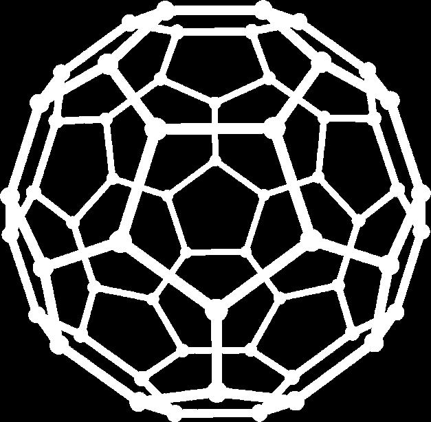
4 The buckyball C60 is referred to as a buckyball and has a distinct shape like a old-style soccer ball Buckyball (part of the fullerene family) Truncated Icosahedron 0.7 nm in diameter with a spacing of 1 nm between adjacent buckyballs Inert Can be made in to superconductor Offshoot studies led to the discovery of the nanotube The most massive particle to show wave-particle duality (Nature 1999)

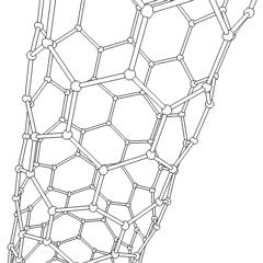
5 The Nanotube Nanotube (part of the fullerene family) Few nm in diameter Length can be as long as it can be made
6 History C60 was produced in 1985 during an experiment to determine what signature carbon molecules might be generated in space Stars have carbon surrounding them The C60 was a unintended by-product Nanotube First observed in 1991, produced in 1992 Interest in buckyball technology shifted to nanotubes (for the most part)
7
8
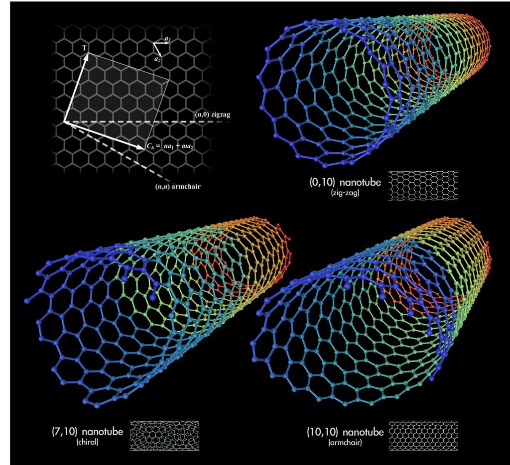
9 Different wraps of the nanotubes produce different results m=n are metallic (armchair above) Others are semiconductors, though there are exceptions Check out Dr. Sinex's Excelets on this
10 Technology at the nanoscale (10-9 meters) Bioengineering Environmental Engineering Bionanosensors Biochips Nanomembranes Nanocatalysts Material Engineering (Mechanical/Civil/Chemical/Aerospace/etc.) Quantum dot Nanocoating
11 Technology at the nanoscale (10-9 meters) Electrical Engineering (Electronics) Lithography (already at nanolevel) DNA chips Nanowires Bionanosensors (yes, this is in Bioengineering) Biochips (yes, this is in Bioengineering) Nano-optics ranges from 1 nm to 100 nm Only one dimension in this range is required to be called nanotechnology Many electronic chips already have components in this range Coatings at this range are commonplace
12 Three types of Wet nanotechnology Water environment Biological Cellular level, membranes Dry nanotechnology Carbon, silicon, other inorganic materials Metals, semiconductors Too reactive; can't operate in wet conditions Computational nanotechnology Modeling and simulation of complete nanostructures Required to understand nanotechnology
13 Surface effects, chemical effects, physical effects are different in the nanoscale then in the macro or micro scale This creates new and interesting products Stain resistant clothes Sweat absorbing clothes This also creates new avenues of research New exciting discoveries wait Some disappointments await as well Nature of research
14 Top-down Build nanotechnology using larger elements No atomic-level control Nanolithography Bottom-up Build from molecular components Components assemble themselves using molecular recognition Self-assembly Needs some for of coding What in nature might be used as a model for this? What are some issues with the use of this?

15 DNA is a coding device that is used in nature DNA is nanometer in size DNA faces: Paul Rothemund
16 spans all disciplines and is too extensive to be done complete here Use examples to try and show some interesting possibilities Wet, dry, and computational Why the understanding of Physics is a must Concepts that are important Scaling laws Quantum mechanics Hartree-Fock Transport phenomena Surfaces Hydrophobic and hydrophilic Diffusion, transport in all dimensions
17 Environment Water Purification Humans need clean consumable water for survival Environmental contaminants are a serious problem to the rescue? Ceramic nanomembrane Ultrafiltration Reactive component (iron oxide ceramic membranes) add an extra-level of removal Aluminum oxide ceramic membranes are another membrane being investigated Iron remediation Nanoscale powder Iron oxidization causes certain organic molecules (including the toxic ones) to break down Nanoscale iron is more reactive then larger iron grains Small size allows it to move between soil particles
18 Materials Nanocrystalline metals What are they? All metals are crystalline with the grain size an important characterization that defines among other things the yield strength Hall-Petch equation (below) Observation of small grain size has suggested increase yield strength, but at levels not consistent with Hall-Petch Implies small grain size gives better yield strength Certainly valid for microcrystalline structures, but questions remain about nanocrystalline structures Cons: Corrosion, creep worse Observed negative Hall-Petch effect Questions remain; studies needed Future shows promise σ y =σ 0 + k 1 2 d σ y = yield strength σ 0 ; k =constant dependant on material
19 Materials Bone Large portion of bone is nanosize hydroxyapatite Repair could be possible using bioactive and resorbable ceramics Mechanism would be osteoinduction
20 Materials Spintronics (or magnetoelectronics) Use the spin of the electron rather then the movement of the electrons For technology the promise is to make faster, smaller transistors So why is this nanotechnology? An electron certainly is not nanometer is it? Technically spintronics is not nanotechnology, however nanotechnology offers the best approach for its practical use Create ferromagnetic semiconductors that require layers that are only a few nanometers ( there you go)
21 Machines Nanoparts are uses for micromachines...an actual nanomachine is less practical Motion is controlled by some form of voltage Nanomotor Using multi-walled nanotubes One tube rotates inside the other In effect have rotational bearings Molecular actuator Nanomotor controlled by the use of a nanocrystal ram Nanoelectromechanical relaxation oscillator Liquid metal droplets exchanging mass Utilizes surface tension (which is very strong)

22 Nanodiamonds
23 Tools Electron microscopes Scanning electron microscope (SEM) Focused beam of electrons Electrons much smaller than1 nm 5 to 10 nm resolution; 1 nm Surface scanner Transmission electron microscope (TEM) Electrons penetrate sample Magnets used to bend the electrons 0.2 nm resolution Analytic electron microscope (AEM) TEM with equipment like spectrometers 0.1 nm resolution Scanning Probe Microscopes (SPM) Uses probes Scanning tunneling microscope (STM) and atomic force microscope (AFM) Nanomanipulators
24 Tools Theory, Modeling, and Simulation (TMS) TMS is most important tool presently Main idea is to study nanotechnology to direct how to use it better Need to interpret data Need models of measuring tools and materials to understand interaction Follows the standard protocol Theory: what do we know about the materials and tools Model: represent our theory in a testable fashion (equations; numerical analysis techniques) Simulate the model to see if it gets us the test results Success use the model to predict some new result Test for new result to confirm model Failure (not computer failure (bugs), but failure of the model) Re-work model Investigate theory
25 is Nanoeverything Nanomaterials Semiconducting nanostructures Buckyballs Nanotubes Nanowires Nanoparticles Metallic nanostructures Nanoelectronics Nano-optics Nanomechanics Nanofluidics etc.
26 PGCC courses that discuss nanotechnology Materials Science course (EGR 2300) General Chemistry for Engineers (CHM 2000) Introductory Engineering's Introduction to module Honors Seminar (EGR 2990) 26
27 PGCC web sites for the excelets (used to support Materials and Chemistry) Materials Science excelets General Chemistry excelets 27
28 PGCC supports (which include some materials science and nanotechnology) PRDM Website - Howard, Cornell, Gallaudet, and PGCC CIQM Website - Harvard, Howard, MIT, Gallaudet, Boston Museum of Science and PGCC
29 websites
30 Materials/ Simulators/Demos/Games Duckboy nanotechnology demonstration Molecular Workbench Microscope Simulators (Windows/Mac OS only)
31 Materials Backup slides for interest only Scale is an important issue in nanotecnology Just compare volume compared to surface area Strength proportional to cross sectional area Weight proportional to volume Strength/weight Elephant ~ 1 Flea ~ 1000
32 Mechanical scaling Mechanics scaling Mass is proportional to volume (think density) Gravitational force is proportional to volume Therefore frictional force is proportional to volume as well, but at very small scale van der Waal forces dominate, therefore striction force is proportional to contact area Spring force is proportional to length Kinetic energy is proportional to volume (mass) Potential energy for gravity is proportional to volume Potential energy for a spring is proportional to area Etc. Hope you get the idea...
33 Molecular Dynamics (MD) Van der Waal forces Covers close range and long range forces Repulsive force and attractive force Describe in MD simulation by Mie-Jones 6-12 or Lennard-Jones 12 6 [ ] vdw V LJ = rij vdw rij Epsilon and sigma are material dependent Epsilon is well depth Sigma is hard repulsion radius
34 Van der Waals revisited Van der Waal forces Note force is derivative of energy Reason Gecko's stick to walls Nanohairs Lots of surface area Beats gravity Keeps us from going through walls We touch things or do we?
35 Scales in Nanorealm Melting point is effected by dimensions 1 D [ ] T m=t m, bulk 1 Where D is in nanometers Imagine 1 nm scale!
36 Scales in Nano-realm An elements bulk crystal structures is not necessarily the same in the nanotechnology realm Ruthenium at 2 to 3 nm can have bcc and fcc (normally hexagonal) Van der Waal interactions dominate
37 Scales in Nano-realm Geometry of wires matter because of volume to surface area ratio High surface-to-volume ratios in nano-realm Gallium nitride < 100 nm will emit different wavelengths of light if having different dimensions (wire, belt, rod)
38 Scales in Nano-realm Porous Materials Zeolites Many tunnels; network of caves Cavities 200 to 2000 pm Pores 300 to 1000 pm Guest molecules (water) 56 zeolites Aluminosilicates most common Metal-organic framework Clay that are like zeolites Up to 4500 sq. meters/g
39 Scales in Nano-realm Porous Materials Zeolites Captures clogging charged Magnesium, Calcium in pores; softens water Sieves (filter) Create catalysts (lots of surface area) Filter & Catalyst better than conventional material Shape-selective catalysis Reactant: only molecules of a given dimension enter and reach the catalyst Product: only molecules of a given dimension get get out Transition state: certain reactions stopped because product is too big for cavity
40 Scales in Nano-realm Small-grain material Grain size determines deformation Plastic deformation equation Hall-Petch equation Where k is constant, d is grain size in micrometers Accurate for grain size 100 nm to 10 micrometers Below 30 nm not accurate At very small size the grain boundaries act more like a web Diffuse, migrate, and slide instead given different effects Probably below 30 nm the material gets brittle, but hard to tell because melting point drops as well...arg! y= o k N where o is frictional stress 2 which oppose dislocation d m
Chapter 12. Nanometrology. Oxford University Press All rights reserved.
 Chapter 12 Nanometrology Introduction Nanometrology is the science of measurement at the nanoscale level. Figure illustrates where nanoscale stands in relation to a meter and sub divisions of meter. Nanometrology
29: Nanotechnology. What is Nanotechnology? Properties Control and Understanding. Nanomaterials
 29: Nanotechnology What is Nanotechnology? Properties Control and Understanding Nanomaterials Making nanomaterials Seeing at the nanoscale Quantum Dots Carbon Nanotubes Biology at the Nanoscale Some Applications
In the name of Allah
 In the name of Allah Nano chemistry- 4 th stage Lecture No. 1 History of nanotechnology 16-10-2016 Assistance prof. Dr. Luma Majeed Ahmed lumamajeed2013@gmail.com, luma.ahmed@uokerbala.edu.iq Nano chemistry-4
Chapter 10. Nanometrology. Oxford University Press All rights reserved.
 Chapter 10 Nanometrology Oxford University Press 2013. All rights reserved. 1 Introduction Nanometrology is the science of measurement at the nanoscale level. Figure illustrates where nanoscale stands
Nanotechnology. Gavin Lawes Department of Physics and Astronomy
 Nanotechnology Gavin Lawes Department of Physics and Astronomy Earth-Moon distance 4x10 8 m (courtesy NASA) Length scales (Part I) Person 2m Magnetic nanoparticle 5x10⁻⁹ m 10 10 m 10 5 m 1 m 10-5 m 10-10
Nanotechnology. Yung Liou P601 Institute of Physics Academia Sinica
 Nanotechnology Yung Liou P601 yung@phys.sinica.edu.tw Institute of Physics Academia Sinica 1 1st week Definition of Nanotechnology The Interagency Subcommittee on Nanoscale Science, Engineering and Technology
Lecture 6: Individual nanoparticles, nanocrystals and quantum dots
 Lecture 6: Individual nanoparticles, nanocrystals and quantum dots Definition of nanoparticle: Size definition arbitrary More interesting: definition based on change in physical properties. Size smaller
Materials. Definitions of nanotechnology. The term nanotechnology was invented by Professor Norio Taniguchi at the University of Tokyo in 1971.
 Materials Definitions of nanotechnology The term nanotechnology was invented by Professor Norio Taniguchi at the University of Tokyo in 1971. The original definition, translated into English Nano-technology'
Lesson 4: Tools of the Nanosciences. Student Materials
 Lesson 4: Tools of the Nanosciences Student Materials Contents Black Box Lab Activity: Student Instructions and Worksheet Seeing and Building Small Things: Student Reading Seeing and Building Small Things:
Nanotechnology Fabrication Methods.
 Nanotechnology Fabrication Methods. 10 / 05 / 2016 1 Summary: 1.Introduction to Nanotechnology:...3 2.Nanotechnology Fabrication Methods:...5 2.1.Top-down Methods:...7 2.2.Bottom-up Methods:...16 3.Conclusions:...19
Jeopardy Q $100 Q $100 Q $100 Q $100 Q $100 Q $200 Q $200 Q $200 Q $200 Q $200 Q $300 Q $300 Q $300 Q $300 Q $300 Q $400 Q $400 Q $400 Q $400 Q $400
 Jeopardy Size and Scale Nano Products Tools Structure Of Matter Science and Society Q $100 Q $200 Q $300 Q $400 Q $500 Q $100 Q $100 Q $100 Q $100 Q $200 Q $200 Q $200 Q $200 Q $300 Q $300 Q $300 Q $300
Nanotechnology. An Introduction
 Nanotechnology An Introduction Nanotechnology A new interdisciplinary field of science The study of systems at the nanoscale The use of tools at the nanoscale Building and applying structures that are
CSCI 2570 Introduction to Nanocomputing
 CSCI 2570 Introduction to Nanocomputing The Emergence of Nanotechnology John E Savage Purpose of the Course The end of Moore s Law is in sight. Researchers are now exploring replacements for standard methods
Chapter 1 Introduction
 Chapter 1 Introduction A nanometer (nm) is one billionth (10-9 ) of a meter. Nanoscience can be defined as the science of objects and phenomena occurring at the scale of 1 to 100 nm. The range of 1 100
Nanostructure. Materials Growth Characterization Fabrication. More see Waser, chapter 2
 Nanostructure Materials Growth Characterization Fabrication More see Waser, chapter 2 Materials growth - deposition deposition gas solid Physical Vapor Deposition Chemical Vapor Deposition Physical Vapor
Introduction to Nanoscience and Nanotechnology
 Introduction to Nanoscience and Nanotechnology ENS 463 by Alexander M. Zaitsev alexander.zaitsev@csi.cuny.edu Tel: 718 982 2812 Office 4N101b 1 What is the size for a nano? 10-3 m, (milli) Macroobjects,
Like space travel and the Internet before it, the possibilities of the nano world catches the imagination of school children and scientists alike.
 The Nano World Preface Nano is the cool thing and it s the buzzword Like space travel and the Internet before it, the possibilities of the nano world catches the imagination of school children and scientists
In today s lecture, we will cover:
 In today s lecture, we will cover: Metal and Metal oxide Nanoparticles Semiconductor Nanocrystals Carbon Nanotubes 1 Week 2: Nanoparticles Goals for this section Develop an understanding of the physical
Kavli Workshop for Journalists. June 13th, CNF Cleanroom Activities
 Kavli Workshop for Journalists June 13th, 2007 CNF Cleanroom Activities Seeing nm-sized Objects with an SEM Lab experience: Scanning Electron Microscopy Equipment: Zeiss Supra 55VP Scanning electron microscopes
RAJASTHAN TECHNICAL UNIVERSITY, KOTA
 RAJASTHAN TECHNICAL UNIVERSITY, KOTA (Electronics & Communication) Submitted By: LAKSHIKA SOMANI E&C II yr, IV sem. Session: 2007-08 Department of Electronics & Communication Geetanjali Institute of Technical
Lesson 1: Introduction to Nanoscience. Teacher Materials
 Lesson 1: Introduction to Nanoscience Teacher Materials Contents Introduction to Nanoscience: Teacher Lesson Plan Introduction to Nanoscience: PowerPoint with Teacher Notes Introduction to Nanoscience
Nanomaterials and their Optical Applications
 Nanomaterials and their Optical Applications Winter Semester 2013 Lecture 02 rachel.grange@uni-jena.de http://www.iap.uni-jena.de/multiphoton Lecture 2: outline 2 Introduction to Nanophotonics Theoretical
Figure 1: Some examples of objects at different size scales ( 2001, CMP Científica, [2])
![Figure 1: Some examples of objects at different size scales ( 2001, CMP Científica, [2])](/thumbs/85/91872790.jpg "Figure 1: Some examples of objects at different size scales ( 2001, CMP Científica, [2])") Top-Down vs. Bottom-Up Nanomanufacturing Prof. Derek J. Hansford, Biomedical Engineering Program and Department of Materials Science & Engineering Learning Objectives: This module should expose the student
Top-Down vs. Bottom-Up Nanomanufacturing Prof. Derek J. Hansford, Biomedical Engineering Program and Department of Materials Science & Engineering Learning Objectives: This module should expose the student
Seminars in Nanosystems - I
 Seminars in Nanosystems - I Winter Semester 2011/2012 Dr. Emanuela Margapoti Emanuela.Margapoti@wsi.tum.de Dr. Gregor Koblmüller Gregor.Koblmueller@wsi.tum.de Seminar Room at ZNN 1 floor Topics of the
Course file PPY15204 Nanoscience and Nanomaterials Table of Contents
 Department Physics Nanotechnology : M.sc Physics Course file PPY15204 Table Contents Second Year MSc Physics (2015-2016 Regulation) Detailed Lesson Plan UNIT-I: INTRODUCTION TO NANOTECHNOLOGY History Importance
Nanotechnology Nanofabrication of Functional Materials. Marin Alexe Max Planck Institute of Microstructure Physics, Halle - Germany
 Nanotechnology Nanofabrication of Functional Materials Marin Alexe Max Planck Institute of Microstructure Physics, Halle - Germany Contents Part I History and background to nanotechnology Nanoworld Nanoelectronics
Nanophysics: Main trends
 Nano-opto-electronics Nanophysics: Main trends Nanomechanics Main issues Light interaction with small structures Molecules Nanoparticles (semiconductor and metallic) Microparticles Photonic crystals Nanoplasmonics
Contents. What is AFM? History Basic principles and devices Operating modes Application areas Advantages and disadvantages
 Contents What is AFM? History Basic principles and devices Operating modes Application areas Advantages and disadvantages Figure1: 2004 Seth Copen Goldstein What is AFM? A type of Scanning Probe Microscopy
There s plenty of room at the bottom! - R.P. Feynman, Nanostructure: a piece of material with at least one dimension less than 100 nm in extent.
 Nanostructures and Nanotechnology There s plenty of room at the bottom! - R.P. Feynman, 1959 Materials behave differently when structured at the nm scale than they do in bulk. Technologies now exist that
Scripts for High School Visits to the Herman Group at Columbia University
 Scripts for High School Visits to the Herman Group at Columbia University Evan Spotte-Smith, Jiayang Hu, and Irving P. Herman April, 2017; updated June, 2017 These presentations were developed for visits
Final Reading Assignment: Travels to the Nanoworld: pages pages pages
 Final Reading Assignment: Travels to the Nanoworld: pages 152-164 pages 201-214 pages 219-227 Bottom-up nanofabrication Can we assemble nanomachines manually? What are the components (parts)? nanoparticles
DocumentToPDF trial version, to remove this mark, please register this software.
 PAPER PRESENTATION ON Carbon Nanotube - Based Nonvolatile Random Access Memory AUTHORS M SIVARAM PRASAD Sivaram.443@gmail.com B N V PAVAN KUMAR pavankumar.bnv@gmail.com 1 Carbon Nanotube- Based Nonvolatile
Investigating Nano-Space
 Name Partners Date Visual Quantum Mechanics The Next Generation Investigating Nano-Space Goal You will apply your knowledge of tunneling to understand the operation of the scanning tunneling microscope.
Nanoparticles and Nanofibers
 Nanoparticles and Nanofibers Why are nanoparticles important? The properties of nanoparticles can be controlled by engineering the size, shape, and composition of the particles. Engineers can incorporate
Inorganic compounds that semiconduct tend to have an average of 4 valence electrons, and their conductivity may be increased by doping.
 Chapter 12 Modern Materials 12.1 Semiconductors Inorganic compounds that semiconduct tend to have an average of 4 valence electrons, and their conductivity may be increased by doping. Doping yields different
Chapter 12 - Modern Materials
 Chapter 12 - Modern Materials 12.1 Semiconductors Inorganic compounds that semiconduct tend to have chemical formulas related to Si and Ge valence electron count of four. Semiconductor conductivity can
How do scientists build something so small? Materials 1 pkg of modeling materials 1 piece of butcher paper 1 set of cards 1 set of markers
 Using Modeling to Demonstrate Self-Assembly in Nanotechnology Imagine building a device that is small enough to fit on a contact lens. It has an antennae and a translucent screen across the pupil of the
There's Plenty of Room at the Bottom
 There's Plenty of Room at the Bottom 12/29/1959 Feynman asked why not put the entire Encyclopedia Britannica (24 volumes) on a pin head (requires atomic scale recording). He proposed to use electron microscope
Image courtesy of Dr James Bendall, University of Cambridge, UK. Discover the secrets h of the Nanoworld
 Image courtesy of Dr James Bendall, University of Cambridge, UK. Discover the secrets h of the Nanoworld Nano has become a buzz word in popular culture to just mean small. To understand nanotechnology
Nanoscale Materials and Their Properties Teacher Guide Unit 2: Metallic and Ionic Nanoparticle
 Nanoscale Materials and Their Properties Teacher Guide Unit 2: Metallic and Ionic Nanoparticles: Extendable Structures Objectives for Metallic and Ionic Nanoparticles: Extendable Structures Lesson Objectives:
SELF-ASSEMBLY AND NANOTECHNOLOGY A Force Balance Approach
 SELF-ASSEMBLY AND NANOTECHNOLOGY A Force Balance Approach Yoon S. Lee Scientific Information Analyst Chemical Abstracts Service A Division of the American Chemical Society Columbus, Ohio WILEY A JOHN WILEY
Nanostructures. Lecture 13 OUTLINE
 Nanostructures MTX9100 Nanomaterials Lecture 13 OUTLINE -What is quantum confinement? - How can zero-dimensional materials be used? -What are one dimensional structures? -Why does graphene attract so much
Table of Content. Mechanical Removing Techniques. Ultrasonic Machining (USM) Sputtering and Focused Ion Beam Milling (FIB)
 Sputtering and Focused Ion Beam Milling (FIB)") Table of Content Mechanical Removing Techniques Ultrasonic Machining (USM) Sputtering and Focused Ion Beam Milling (FIB) Ultrasonic Machining In ultrasonic machining (USM), also called ultrasonic grinding,
Table of Content Mechanical Removing Techniques Ultrasonic Machining (USM) Sputtering and Focused Ion Beam Milling (FIB) Ultrasonic Machining In ultrasonic machining (USM), also called ultrasonic grinding,
SPECIFIC USES OR APPLICATIONS OF NANOSTRUCTURES; MEASUREMENT OR ANALYSIS OF NANOSTRUCTURES; MANUFACTURE OR TREATMENT OF NANOSTRUCTURES
 CPC - B82Y - 2017.08 B82Y SPECIFIC USES OR APPLICATIONS OF NANOSTRUCTURES; MEASUREMENT OR ANALYSIS OF NANOSTRUCTURES; MANUFACTURE OR TREATMENT OF NANOSTRUCTURES Definition statement This place covers:
Basic Laboratory. Materials Science and Engineering. Atomic Force Microscopy (AFM)
") Basic Laboratory Materials Science and Engineering Atomic Force Microscopy (AFM) M108 Stand: 20.10.2015 Aim: Presentation of an application of the AFM for studying surface morphology. Inhalt 1.Introduction...
Basic Laboratory Materials Science and Engineering Atomic Force Microscopy (AFM) M108 Stand: 20.10.2015 Aim: Presentation of an application of the AFM for studying surface morphology. Inhalt 1.Introduction...
Instrumentation and Operation
 Instrumentation and Operation 1 STM Instrumentation COMPONENTS sharp metal tip scanning system and control electronics feedback electronics (keeps tunneling current constant) image processing system data
Scanning Tunneling Microscopy
 Scanning Tunneling Microscopy References: 1. G. Binnig, H. Rohrer, C. Gerber, and Weibel, Phys. Rev. Lett. 49, 57 (1982); and ibid 50, 120 (1983). 2. J. Chen, Introduction to Scanning Tunneling Microscopy,
DOWNLOAD OR READ : NANOSTRUCTURED MATERIALS PROCESSING PROPERTIES AND APPLICATIONS 2ND ENLARGED EDITION PDF EBOOK EPUB MOBI
 DOWNLOAD OR READ : NANOSTRUCTURED MATERIALS PROCESSING PROPERTIES AND APPLICATIONS 2ND ENLARGED EDITION PDF EBOOK EPUB MOBI Page 1 Page 2 nanostructured materials processing properties and applications
= 6 (1/ nm) So what is probability of finding electron tunneled into a barrier 3 ev high?
 So what is probability of finding electron tunneled into a barrier 3 ev high?") STM STM With a scanning tunneling microscope, images of surfaces with atomic resolution can be readily obtained. An STM uses quantum tunneling of electrons to map the density of electrons on the surface
STM STM With a scanning tunneling microscope, images of surfaces with atomic resolution can be readily obtained. An STM uses quantum tunneling of electrons to map the density of electrons on the surface
Nanotechnology for Ground Improvement. Amro El Badawy, Ph.D. W.M. Keck Foundation Postdoctoral Fellow Global Waste Research Institute Jan 27 th, 2015
 Nanotechnology for Ground Improvement Amro El Badawy, Ph.D. W.M. Keck Foundation Postdoctoral Fellow Global Waste Research Institute Jan 27 th, 2015 Who cares about nanotechnology?!! Soil Stabilization
Fabrication at the nanoscale for nanophotonics
 Fabrication at the nanoscale for nanophotonics Ilya Sychugov, KTH Materials Physics, Kista silicon nanocrystal by electron beam induced deposition lithography Outline of basic nanofabrication methods Devices
Nanotechnology where size matters
 Nanotechnology where size matters J Emyr Macdonald Overview Ways of seeing very small things What is nanotechnology and why is it important? Building nanostructures What we can do with nanotechnology?
ME 4875/MTE C16. Introduction to Nanomaterials and Nanotechnology. Lecture 2 - Applications of Nanomaterials + Projects
 ME 4875/MTE 575 - C16 Introduction to Nanomaterials and Nanotechnology Lecture 2 - Applications of Nanomaterials + Projects 1 Project Teams of 4 students each Literature review of one application of nanotechnology
Scale, structure and behaviour
 Scale, structure and behaviour Lecture 2 MTX9100 Nanomaterjalid OUTLINE -How are crystals structured? -Why and how does nanoworld differ from the world we live in? -When does size matter? What is the smallest
Matter and Energy. Section 2.1 Chapter 2. Representations of Matter: Models and Symbols. Goal 1. Goal 2
 Section 2.1 Chapter 2 Matter and Energy Representations of Matter: Models and Symbols Goal 1 Goal 2 Identify and explain the difference among observations of matter at the macroscopic, microscopic, and
CHAPTER 11 Semiconductor Theory and Devices
 CHAPTER 11 Semiconductor Theory and Devices 11.1 Band Theory of Solids 11.2 Semiconductor Theory 11.3 Semiconductor Devices 11.4 Nanotechnology It is evident that many years of research by a great many
Nanoscale optical circuits: controlling light using localized surface plasmon resonances
 Nanoscale optical circuits: controlling light using localized surface plasmon resonances T. J. Davis, D. E. Gómez and K. C. Vernon CSIRO Materials Science and Engineering Localized surface plasmon (LSP)
Biomaterial Scaffolds
 Biomaterial Scaffolds Biomaterial Properties Surface properties Bulk properties Biological properties Types of Biomaterials Biological materials Synthetic materials Surface Properties The body reads the
Challenges for Materials to Support Emerging Research Devices
 Challenges for Materials to Support Emerging Research Devices C. Michael Garner*, James Hutchby +, George Bourianoff*, and Victor Zhirnov + *Intel Corporation Santa Clara, CA + Semiconductor Research Corporation
Nanotechnology: Today and tomorrow
 Nanotechnology: Today and tomorrow Horst-Günter Rubahn NanoSYD Mads Clausen Instituttet Syddansk Universitet Alsion 2 6400 Sønderborg Agenda Alsion A bit about nano Nanoproducts Top down vs. bottom up
INTRODUCTION TO SCA\ \I\G TUNNELING MICROSCOPY
 INTRODUCTION TO SCA\ \I\G TUNNELING MICROSCOPY SECOND EDITION C. JULIAN CHEN Department of Applied Physics and Applied Mathematics, Columbia University, New York OXFORD UNIVERSITY PRESS Contents Preface
Computers of the Future? Moore s Law Ending in 2018?
 Computers of the Future? CS 221 Moore s Law Ending in 2018? Moore s Law: Processor speed / number transistors doubling approximately 18 months 1 Moore s Law Moore s Law Recent research predicts an end
PHY 481/581. Some classical/quantum physics for the nanometer length scale.
 PHY 481/581 Some classical/quantum physics for the nanometer length scale http://creativecommons.org/licenses/by-nc-sa/3.0/ 1 What is nano-science? the science of materials whose properties scale with
General concept and defining characteristics of AFM. Dina Kudasheva Advisor: Prof. Mary K. Cowman
 General concept and defining characteristics of AFM Dina Kudasheva Advisor: Prof. Mary K. Cowman Overview Introduction History of the SPM invention Technical Capabilities Principles of operation Examples
Nanotechnology? Source: National Science Foundation (NSF), USA
, USA") 2 2 Nanotechnology? Ability to work at the atomic, molecular and even sub-molecular levels in order to create and use material structures, devices and systems with new properties and functions Source:
2 2 Nanotechnology? Ability to work at the atomic, molecular and even sub-molecular levels in order to create and use material structures, devices and systems with new properties and functions Source:
Scanning Probe Microscopy. Amanda MacMillan, Emmy Gebremichael, & John Shamblin Chem 243: Instrumental Analysis Dr. Robert Corn March 10, 2010
 Scanning Probe Microscopy Amanda MacMillan, Emmy Gebremichael, & John Shamblin Chem 243: Instrumental Analysis Dr. Robert Corn March 10, 2010 Scanning Probe Microscopy High-Resolution Surface Analysis
Scanning Force Microscopy
 Scanning Force Microscopy Roland Bennewitz Rutherford Physics Building 405 Phone 398-3058 roland.bennewitz@mcgill.ca Scanning Probe is moved along scan lines over a sample surface 1 Force Microscopy Data
1.1. Introduction to Nanoscience and Nanotechnology
 1.1. Introduction to Nanoscience and Nanotechnology 1.1.1. A Brief Historical Overview Before trying to understand and discuss about synthesis, characterization and application of nanomaterials, it is
MODULE 2 : FOUNDATIONS IN BIOLOGY
 OCR A LEVEL BIOLOGY MODULE 2 : FOUNDATIONS IN BIOLOGY REVISION NOTES For 2015 onwards specification Miss T Banda All living things are primarily made from 4 key elements: Carbon (C) Hydrogen (H) Oxygen
Confocal Microscope Imaging of Single-Emitter Fluorescence and Photon Antibunching
 Confocal Microscope Imaging of Single-Emitter Fluorescence and Photon Antibunching By Dilyana Mihaylova Abstract The purpose of this lab is to study different types of single emitters including quantum
Monolayer Semiconductors
 Monolayer Semiconductors Gilbert Arias California State University San Bernardino University of Washington INT REU, 2013 Advisor: Xiaodong Xu (Dated: August 24, 2013) Abstract Silicon may be unable to
A NEW APPROACH TOWARDS PROPERTY NANOMEASUREMENTS USING IN-SITU TEM
 A NEW APPROACH TOWARDS PROPERTY NANOMEASUREMENTS USING IN-SITU TEM Z.L. WANG*, P. PONCHARAL**, W.A. DE HEER** and R.P. GAO* * School of Materials Science and Engineering, ** School of Physics, Georgia
Welcome to NANO* 2000
 Lecture Zero Welcome to NANO* 2000 First - the "big picture" of the course and the course outline -grading scheme - exam schedule - review paper - lab (Jay) last revision September 4 2013: MDB 0-1 NANO*
AP BIOLOGY CHAPTERS 1-3 WORKSHEET
 Name Date AP BIOLOGY CHAPTERS 1-3 WORKSHEET MULTIPLE CHOICE. 33 pts. Place the letter of the choice that best completes the statement or answers the question in the blank. 1. Which of the following sequences
The Biological Importance of Water
 The Biological Importance of Water Why is water important? Major component of all living systems and our planet. Occupies most of a cells volume. Has major properties that living systems require. Water
PV Tutorial Allen Hermann, Ph. D. Professor of Physics Emeritus, and Professor of Music Adjunct, University of Colorado, Boulder, Colorado, USA and
 PV Tutorial Allen Hermann, Ph. D. Professor of Physics Emeritus, and Professor of Music Adjunct, University of Colorado, Boulder, Colorado, USA and Vice-president, NanoTech Inc. Lexington, Kentucky, USA
3.30 TITANIUM DIOXIDE
 181 3.30 TITANIUM DIOXIDE Technology Prospects Addressable market size 5 Competitive landscape 3 IP landscape 4 Commercial prospects 4 Technology drawbacks 3 Total score (out of max. 25): 19 3.30.1 Properties
master thesis STM studies of molecules for molecular electronics
 STM studies of molecules for molecular electronics Experimental study of single organic molecules by Scanning Tunneling Microscope (STM) and spectroscopy at low temperature Experimental STM images of Aza-BODIPY
Techniken der Oberflächenphysik (Techniques of Surface Physics)
") Techniken der Oberflächenphysik (Techniques of Surface Physics) Prof. Yong Lei & Dr. Yang Xu Fachgebiet 3D-Nanostrukturierung, Institut für Physik Contact: yong.lei@tu-ilmenau.de yang.xu@tu-ilmenau.de
Techniken der Oberflächenphysik (Techniques of Surface Physics) Prof. Yong Lei & Dr. Yang Xu Fachgebiet 3D-Nanostrukturierung, Institut für Physik Contact: yong.lei@tu-ilmenau.de yang.xu@tu-ilmenau.de
Understanding the properties and behavior of groups of interacting atoms more than simple molecules
 Condensed Matter Physics Scratching the Surface Understanding the properties and behavior of groups of interacting atoms more than simple molecules Solids and fluids in ordinary and exotic states low energy
The application of nano aluminum powder on solid propellant
 The application of nano aluminum powder on solid propellant Metal incendiary agent is one of the important components of modern solid propellant, which can improve the explosion heat and density of propellant.
Plasmonics. The long wavelength of light ( μm) creates a problem for extending optoelectronics into the nanometer regime.
 creates a problem for extending optoelectronics into the nanometer regime.") Plasmonics The long wavelength of light ( μm) creates a problem for extending optoelectronics into the nanometer regime. A possible way out is the conversion of light into plasmons. They have much shorter
Plasmonics The long wavelength of light ( μm) creates a problem for extending optoelectronics into the nanometer regime. A possible way out is the conversion of light into plasmons. They have much shorter
Fission and Chain Reactions
 The Harnessed Atom Lesson Five Fission and Chain Reactions What you need to know about Fission and Chain Reactions: Fission Chain reaction Uranium fuel Mining Milling Enrichment Fuel fabrication 2 Nuclear
Introduction to Nanotechnology Chapter 5 Carbon Nanostructures Lecture 1
 Introduction to Nanotechnology Chapter 5 Carbon Nanostructures Lecture 1 ChiiDong Chen Institute of Physics, Academia Sinica chiidong@phys.sinica.edu.tw 02 27896766 Carbon contains 6 electrons: (1s) 2,
Single-Molecule Recognition and Manipulation Studied by Scanning Probe Microscopy
 Single-Molecule Recognition and Manipulation Studied by Scanning Probe Microscopy Byung Kim Department of Physics Boise State University Langmuir (in press, 2006) swollen collapsed Hydrophilic non-sticky
Contents. Foreword by Darrell H. Reneker
 Table of Foreword by Darrell H. Reneker Preface page xi xiii 1 Introduction 1 1.1 How big is a nanometer? 1 1.2 What is nanotechnology? 1 1.3 Historical development of nanotechnology 2 1.4 Classification
PHYS 3313 Section 001 Lecture #21 Monday, Nov. 26, 2012
 PHYS 3313 Section 001 Lecture #21 Monday, Nov. 26, 2012 Superconductivity Theory, The Cooper Pair Application of Superconductivity Semi-Conductor Nano-technology Graphene 1 Announcements Your presentations
Chapter 10: Liquids, Solids, and Phase Changes
 Chapter 10: Liquids, Solids, and Phase Changes In-chapter exercises: 10.1 10.6, 10.11; End-of-chapter Problems: 10.26, 10.31, 10.32, 10.33, 10.34, 10.35, 10.36, 10.39, 10.40, 10.42, 10.44, 10.45, 10.66,
CH676 Physical Chemistry: Principles and Applications. CH676 Physical Chemistry: Principles and Applications
 CH676 Physical Chemistry: Principles and Applications History of Nanotechnology: Time Line Democritus in ancient Greece: concept of atom 1900 : Rutherford : discovery of atomic nucleus The first TEM was
Introduction to the Scanning Tunneling Microscope
 Introduction to the Scanning Tunneling Microscope A.C. Perrella M.J. Plisch Center for Nanoscale Systems Cornell University, Ithaca NY Measurement I. Theory of Operation The scanning tunneling microscope
Lecture 4 Scanning Probe Microscopy (SPM)
") Lecture 4 Scanning Probe Microscopy (SPM) General components of SPM; Tip --- the probe; Cantilever --- the indicator of the tip; Tip-sample interaction --- the feedback system; Scanner --- piezoelectric
Lecture 4 Scanning Probe Microscopy (SPM) General components of SPM; Tip --- the probe; Cantilever --- the indicator of the tip; Tip-sample interaction --- the feedback system; Scanner --- piezoelectric
Nano-mechatronics. Presented by: György BudaváriSzabó (X0LY4M)
") Nano-mechatronics Presented by: György BudaváriSzabó (X0LY4M) Nano-mechatronics Nano-mechatronics is currently used in broader spectra, ranging from basic applications in robotics, actuators, sensors,
Nano-mechatronics Presented by: György BudaváriSzabó (X0LY4M) Nano-mechatronics Nano-mechatronics is currently used in broader spectra, ranging from basic applications in robotics, actuators, sensors,
CHARACTERIZATION of NANOMATERIALS KHP
 CHARACTERIZATION of NANOMATERIALS Overview of the most common nanocharacterization techniques MAIN CHARACTERIZATION TECHNIQUES: 1.Transmission Electron Microscope (TEM) 2. Scanning Electron Microscope
NanoExposed! Chemical Applications in Nanotechnology
 NanoExposed! Chemical Applications in Nanotechnology Priscilla Hill 1 Abstract As part of an NSF NUE grant, the introductory seminar course NanoExposed! was developed to introduce freshmen to basic concepts
CORE MOLIT ACTIVITIES at a glance
 CORE MOLIT ACTIVITIES at a glance 1. Amplification of Biochemical Signals: The ELISA Test http://molit.concord.org/database/activities/248.html The shape of molecules affects the way they function. A test
How To Grow a Super Material or Troubleshoot a Classic One
 How To Grow a Super Material or Troubleshoot a Classic One David A. Muller APPLIED AND ENGINEERING PHYSICS Being able to see each atom of a material has allowed us to troubleshoot, discover, and create
Chapter 6 Magnetic nanoparticles
 Chapter 6 Magnetic nanoparticles Magnetic nanoparticles (MNPs) are a class of nanoparticle which can be manipulated using magnetic field gradients. Such particles commonly consist of magnetic elements
The Dielectric Function of a Metal ( Jellium )
") The Dielectric Function of a Metal ( Jellium ) Total reflection Plasma frequency p (10 15 Hz range) Why are Metals Shiny? An electric field cannot exist inside a metal, because metal electrons follow the
The Dielectric Function of a Metal ( Jellium ) Total reflection Plasma frequency p (10 15 Hz range) Why are Metals Shiny? An electric field cannot exist inside a metal, because metal electrons follow the
The Science and Engineering of Materials, 4 th ed Donald R. Askeland Pradeep P. Phulé. Chapter 2 Atomic Structure
 The Science and Engineering of Materials, 4 th ed Donald R. Askeland Pradeep P. Phulé Chapter 2 Atomic Structure Objectives of Chapter 2 The goal of this chapter is to describe the underlying physical
672 Advanced Solid State Physics. Scanning Tunneling Microscopy
 672 Advanced Solid State Physics Scanning Tunneling Microscopy Biao Hu Outline: 1. Introduction to STM 2. STM principle & working modes 3. STM application & extension 4. STM in our group 1. Introduction