Hydrogen Ion-Implantation in Smart- Cut SOI Fabrication Technique Term Project Joy Johnson
|
|
|
- Brian Lambert
- 6 years ago
- Views:
Transcription
1 Hydrogen Ion-Implantation in Smart- Cut SOI Fabrication Technique
2 1. INTRODUCTION Hydrogen Ion-Implantation in Smart-Cut SOI Fabrication Technique A decade ago, the Smart-Cut process was introduced as a technology so revolutionary and unconventional in the production of thin films that every sector of the semiconductor industry attempted to use it for one application or another. However, today the primary application of this process is that of fabricating Silicon-On-Insulator (SOI) wafers which have become the foundation for ultra-large-scale integration (ULSI) device structures as shown in Appendix A. The Smart-Cut process was created by Bruel, Aspar, et al at LETI to obtain delamination of a thin layer in a thick substrate [1]. The process is advantageous in the production of SOI wafers, because it enables greater uniformity of the top Silicon layer while preserving its good crystal quality. Most importantly, this process is able to meet the criteria necessary for development of recent ULSI technologies which include thickness homogeneity, good crystalline quality, low cost, and excellent electrical properties while using standard equipment. In comparison with other SOI fabrication processes, it is particularly advantageous because it is relatively simple to ramp into industry and only requires one wafer to complete the SOI process. Smart-Cut processes also provided additional evidence into the power of the use of ion beam. 2. SMART-CUT PROCESS Smart-Cut process is indeed revolutionary, but what makes it so original is that it exploits the "basic physical phenomenon related to blistering, i.e. creation of microcavities, as a way of inducing in-depth splitting at the range of implanted protons over the whole wafer. [1] The process has four key steps described in detail below: Step 1: Wafer A is capped with a thin dielectric layer of thermally grown SiO 2 which will serve as the buried oxide of the SOI structure. Then, Hydrogen ion implantation is performed on
3 the wafer at a dosage range from 3e16-1e17cm- 2 while keeping the substrate temperature in the range from 225 to ~300 C. Step 2: Wafer A and a handle wafer B are cleaned using a modified RCA clean. Hydrophilic bonding is performed at room temperature of wafer A to wafer B (which is also oxide capped or bare). Then, the bonded wafers are checked to be void-free using infra-red spectroscopy and magic mirror observations. Wafer B plays a pivotal role in the process by serving as a stiffener and the bulk Silicon under the buried oxide of the SOI structure. Step 3: The bonded wafers undergo a two-phase heat treatment. The first phase occurs from C and during this phase the implanted wafer A splits into two parts: a thin monocrystalline layer of Silicon still bonded to wafer B as a SOI structure and the rest of wafer A which can be recycled and used as a handle wafer again. The split takes place because of phenomena of blistering and flaking induced by the hydrogen implantation, as shown in Appendix B. The SOI structure's upper layer is gained through this split at the hydrogen concentration depth (Rp). The second phase occurs at 1100 C to strengthen the chemical bonds. Step 4: The new structure is touch polished using chemical mechanical polishing (CMP) since after splitting the upper layer of the SOI structure has a surface micro roughness that has to be reduced. 2.1 Explanation of Focus Of the four primary steps in the Smart-Cut process, "the use of ion implantation and the formation of a buried damaged layer along which splitting of a wafer occurs are the key links of the Smart-Cut technology."[1] For the purposes of this project, I will be narrowing my focus to the hydrogen implantation done in Step 1. Particularly focusing on the role that the hydrogen ion-implantation and respective variants play in inducing the exfoliation, blistering, or creation
4 of microcavities and flaking which cause the in-depth splitting at the range of implanted ions over the wafer. From the literature there are two primary methods in which to produce the afore mentioned physical phenomena. The first method is by performing a high-dose implantation, causing the blistering to be visible at around 2e17cm- 2 and the flaking as the dose increases. The second method, which is currently used in the Smart-Cut process, is that of medium-dose implantation and annealing. This is a two-step process in which the former performs a limited hydrogen dose implantation (from 3e16cm- 2 to 1e17cm- 2 2) which allows for a layer of gaseous microbubbles to form in the lower region of the wafer and the latter performs a thermal treatment (400 C-600 C) which causes the blistering and flaking. The microbubbles grow due to Ostwald ripening and ultimately supply the internal force necessary to cause the cleavage in the hydrogen-implanted wafer[14]. Its generally accepted that the microbubbles occur at the peak in the hydrogen ion-implantation concentration profile and appear physically along the (100) plane parallel to the surface. 2.2 Previous Findings on Hydrogen Implant to Damage Relationship According to Choyke et al, high dosage proton implants cause extreme ion bombardments which in turn cause the macroscopic physical effects mentioned. Using this knowledge, much of the literature notes that the use of damage energy calculations, primarily from backscattering and channeling (in addition to recoiling atoms, cascades, etc) can be used in analysis of the hydrogen ion implantation step and its role in inducing splitting at the projected range. The use of a seemingly problematic physical phenomenon is what makes the Smart-Cut process so unconventional, but it is also the source of many of the complaints of the process as we will examine in section 3.
5 There have been a few previous studies on the general damage of hydrogen implantation which extract damage profiles on the assumptions that scattering and dechanneling can be thought to originate from random displaced silicon atoms at a given depth and that the defect distribution is the same as the damage energy distribution. Chu et al found that as the implant energy was decreased, the backscattering yield is slightly decreased [9]. Additionally, as expected for most ion implantation profiles, as the implant energy increased they saw an indirect relationship with projected range (Rp), or depth. Using Ziegler's method, they also find a relatively direct relationship between defect concentration and the implant energy. I will test this with a comparison of the percentage of the silicon atoms randomly displaced from the lattice site, which the relative scale is cited in the article, with added complexity of dosage and tilt variation. In all of the papers I have reviewed on this topic there have been very narrow range and damage distributions which can be attributed to many overshot predictions of stopping power. As well the depth distributions have been deeper than normal B or As profiles, but this can be easily explained by the fact that H is a light ion which will cause it to travel farther and have a broader distribution. In conclusion, the general consensus of the literature confirmed by Höchbauer et al is that the generation of the gaseous microbubbles and subsequent cleavage is contingent upon lattice damage resulting from the hydrogen ion-implantation [10]. 3. PRIOR RESEARCH AND PROBLEMS The Smart-Cut process solves many problems that other methods of fabricating SOI wafers create, however it presents its own problems as well. Smart-Cut leaves a final thickness of the device layer "not easily controlled due to polishing to remove the surface roughness"[8], thus there has to be an abbreviated Smart-Cut process that addresses this by accurately
6 controlling the thickness variations, possibly without a polishing operation. Additionally, there needs to be a process of SOI wafer fabrication where uniformity and thickness of the SOI device layer are independently controlled and selected. There has been such a process proposed, with an etch stop layer beneath the device layer, avoiding CMP and controlling the uniformity and thickness of the device layer [8]. The need for uniformity and control of the final thickness of the device layer is the primary problem found in the literature, showing as one of few, the lack of research into the fundamental mechanisms and relationships of this process. As of 2004, there has been lack of in-depth studies on this technology and thus a lack in the fundamental understanding of the Smart-Cut Process basic mechanisms and any knowledge gained at this level will be significantly beneficial for further production process development and large-scale implementation of this novel technique. [7] So, my simulations will seek to be a comprehensive overview of all of the existing relationships between the key variants in Step 1; those being implant energy, dosage, depth (Rp), damage energy, tilt and their subsequent effect on the splitting and/or cleavage mechanism. 4. SIMULATIONS & RESULTS At a range of different implant energies (85-200keV) I will examine changes in the projected range (in some cases depth), the 3 other moments of the ion distribution, defect distribution, and ion spatial arrangement as I vary the implant energy, tilt and dosage. Primarily these simulations will serve as a verification of relationships that exist between the variants that can be enhanced in the Smart-Cut process, since the projected range and defect distribution determine where and how effective the physical phenomena of splitting occurs in the SOI structure.
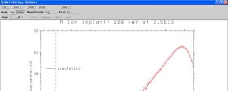
7 4.1 SIMULATION SETUP TSUPREM-4 Simulations Initially, I decided to perform simulations in TSUPREM-4, however this program does not have a direct method for modeling hydrogen ion implantation thus, I used the New Impurity functionality to create a hydrogen impurity using its atomic weight and number, as well as its diffusion impurity coefficients on oxide from other readings (DIX.0=0.5, DIX.E=3.4). I modeled two other well-known elements that are normal to TSUPREM-4, those being Boron and Arsenic as shown in the code in Appendix H and then implemented the new Hydrogen impurity. In TSUPREM-4, initially I gave the implant model the dosage and ideal energy commonly found in the literature [8], 3.5e16/cm 2 and 95keV and the Monte Carlo parameter an input of N.ION= in order to more accurately compare it with my TRIM output. I also assumed that the SiO 2 capped layer was 150nm, because that is the accepted capping thickness for SiO 2 layers and no papers actually specified a thickness. (Fitted values for Lattice Binding Energy (2), Surface Binding Energy (4.7), Displacement Energy (15)). My input code includes the thermal growth of the SiO 2 in addition to the Hydrogen ion implantation as shown in Appendix G. I decided to use the Monte Carlo ion implant model in TSUPREM4 which models the crystal to amorphous transition that occurs during ion implantation including the effects primarily of reflected ions and damage from vacancies and interstitials. I plan to use it to find the dependency of dose, depth, and energy on the effectiveness of creating the cavities for the Smart- Cut process by looking at the effects of the afore mentioned variants on the implantation profile/distribution. This form of Monte Carlo calculations are limited in functionality in that they are a superset of Monte Carlo ion implantation functionality of the process simulator PEPPER. The calculations used in TSUPREM-4 are under the primary assumption that the ions
8 involved in implantation lose energy through two processes: nuclear scattering and interactions with the electrons of the target atoms. Nuclear scattering is the process based on binary collision theory, in which the nucleus of an ion elastically scatters off the nucleus of a target atom. The latter is the interaction of the ion with the electrons of the target atoms; this is an inelastic process which does not alter the ion s direction of motion TRIM Simulations In the literature there was also modeling done using TRIM92 so I decided to also investigate using this software. SRIM is the umbrella of the programs, of which TRIM is a part of. TRIM calculates the stopping and range of ions into a substrate through the use of quantum mechanical handling of ion-target atom collisions. The calculation is much more accurate and efficient than that of TSUMPREM-4, because any material can be set up for calculation and the calculation is efficiently done through the use of statistical algorithms which allow the ions to jump between collisions be calculated and then averaged over gaps. Long range interactions are described by including the target's collective electronic structure and interatomic bond structure [9] when the calculation is setup (tables of nominal values are supplied). More specifically, Monte Carlo Transport Calculation of ion interactions with multi-layer complex targets, is done under the TRIM program. TRIM is one of the most comprehensive software programs of its kind, in that it can accept complex targets with up to eight different layers and will calculate the 3D final distribution of the ions as well as the kinetic phenomena of ion energy loss, including target damage, ionization, etc. I set up the TRIM program on the GUI much like I did the TSUPREM-4 code I wrote,: I Setup the ion to be Hydrogen on a SiO 2 capped layer that was 150nm. I specified tilt and implant energy since those are the only inputs allowed by TRIM (Temperature and dose cannot be
9 specified or adjusted). After running the simulation, I pulled plots of the Ion Range, Ion Track, Damage Events, and Collision Events as shown in Appendices C-F. 4.2 Simulation Outcomes I used the following matrix of variants for the TRIM Monte Carlo Calculations using the Detailed Calculation with full Damage Cascades Option which follows every recoil above the lowest displacement energy of the target atom, carefully calculated at 100,000 ions. Tables 1 & 2 below give a summary of the Ion Range Distributions and Profiles shown in Appendix C. Table 1. TRIM Monte Carlo Simulation Outputs at 0 Tilt Ion Range (Rp) (Ǻ) Straggle (Ǻ) (σ) Skewness (γ) Kurtosis (β) Implant Energy (kev) * * Backscattered Ions Table 2. TRIM Monte Carlo Simulation Outputs at 5 Tilt Ion Range (Rp) (Ǻ) Straggle (Ǻ) (σ) Skewness (γ) Kurtosis (β) Implant Energy (kev) * Backscattered Ions
10 200* *These values may be slightly inaccurate b/c of such high dosage in a light ion implantation; Must be repeated by Surface Sputtering/Monolayer Collisions calculations instead of the Detailed Calculation with full Damage Cascades however these calculations can take >10hours to complete, causing my machine to timeout. Each of the four moments in Tables 1 & 2 can be calculated using the following formulas. (1) As shown in the tables, the Ion Range and Straggle both increase as a function of implant energy which verifies Bruel et al s assumptions [3]. From the Ion Range plots, I took the Ion Ranges in (atoms/cm3/atoms/cm2) to predict impurity concentration at a specific implant dose, using the simple formula: atoms cm^3 ions atoms IONRanges * IMPLANTATIONDose = IMPURITYConcentration (2) atoms cm^2 cm^3 cm^2
11 to examine the change in the ion distribution with the variation in implantation energies as well as tilt angle from the Table 1 of Variants. Table 3 gives a summary of plots from TSUPREM-4 simulations in Appendix G. Table 3. TSUPREM-4 Monte Carlo Simulation Outputs of Ion Range (um) Dosage of 2e17 cm -2 Ion Implant Energy (kev) Dosage of 3.5e16 cm -2 For the TSUPREM-4 simulations at a dose of 2e17 cm -2, the ion range in Table 4 at with an impurity concentration ~10 22 cm -3 and the simulations at a dose of 3.5e16 cm -3 show an impurity concentration ~10 21 cm -3 proving that I was able to replicate the original graphs of M.Bruel, et al [3]. Additionally, it verifies that irregardless of dosage ion implant energy has a direct relationship with ion range or depth. 4.3 Comparison of Simulations (TSUPREM-4 & TRIM) Table 4. Comparison of achieved Ion Range(um) in TSUPREM-4 and TRIM simulations at ideal dosage, 3.5e16 cm -2. TSUPREM-4 Ion Range TRIM Ion Range Ion Implant Energy (kev)
12 * *.78 From Table 4, we can also deduce using the back of the envelope formula (2) that the impurity concentration at which these values were achieved in TRIM was one order of magnitude different than that of TSUPREM-4 (~10 21 vs. ~10 22, respectively). 5. CONCLUSION Through the use of my Monte Carlo simulations in both TRIM and TSUPREM-4, I was able to characterize many of the relationships present in the Hydrogen ion-implantation in Step 1 of the Smart-Cut process. Through the TRIM simulations of the Ion Ranges, I was able to generate the ion profiles/distributions which show the direct relationship between implant energy and depth. As shown in Appendix C and Table 1, one can see as the energy is increased from 85keV to 200keV the depth is increased (The 175keV and 200 kev graphs had to be regenerated using Surface Sputtering/Monolayer Collision Steps due to TRIM s use of the concept of free flight paths for the ions causing anomalous peaks and dips in our graph. ) One can also see that the profiles are slightly skewed toward the surface similar to the simulated profiles for Boron, since both are relatively light ions and more likely to backscatter off the silicon atoms. This relationship is only slightly shifted due to the change in tilt from 0 to 5 [Appendix C], the tilt can affect the number
13 of ions channeled in certain crystalline orientations as well as cause the implanted profiles to have a reduced number of incident ions and be foreshortened. The depth is only decreased on average by approx. 30 Ǻ, causing me to assume that there is very little change actually caused by a change in tilt with the exception of foreshortening, and the direct relationship between implant energy and depth is maintained. Specifically, at the ideal energy of 95keV, the range at 0 tilt is 8062 Ǻ and the range at 5 tilt is 8033 Ǻ. Additionally from the TRIM simulations in Appendix D which generated the damage events, namely target displacements, which from the Chu papers [9] can be used to examine the defect distribution. Defect concentration can be expressed as the amount of Silicon atoms displaced from the lattice site. So as we examine the target displacements we are looking at a relative estimate of defect concentration and since we know that the defects are what cause the physical phenomena at the Smart-cut layer to be split we can determine best fit parameters for that occurrence. In Appendix D, I recreate similar defect distributions to those in Chu s paper, showing that in effect the defect concentration occurs at a greater depth for higher energy implants, so the physical phenomena and splitting will take place at a greater depth as well. At the ideal energy of 95keV, the defect concentration peaks around 0.75um according to both my simulation and Chu s paper. An additional observation that can be made from the TRIM simulations in Table 1 and Table 2 is that when there is no tilt, the number of backscattered ions is at a maximum at the ideal 95keV. From the literature we know that the damage energy includes backscattering in its calculations and this damage energy is directly related to predictability of the physical phenomena that enable the Smart-cut splitting mechanism. Regardless of the tilt, Tables 1 and 2 verify that straggle and projected range increase as a function of implant energy. In Appendices
14 D and E, I also observed the movement in the number of displacements and vacancies to greater depths with greater ion implant energy which proves the assumption that damage energy components help to determine the depth at which the physical phenomena of the Smart-Cut process occurs. It should also be noted that from Appendix F, the Ion Track in TRIM shows that regardless of the tilt, the ions behave radially and spatially in the same fashion, the only change is the actual shift in depth at which they are implanted. I also repeated parallel simulations in TSUPREM-4 to generate the ion profiles and verify the relationships that I observed in TRIM. I was able to verify that as in TRIM, implant energy and ion range/depth have a strong direct relationship. I was also able to show (Table 4) that this relationship is irregardless of dose. Dosage only affected the projected range of implanted H ions, and not as drastically as has been previously assumed. Also I was able to show that the ideal 3.5e16 cm -3 dosage gave a better profile than that of the high dosage version, proving the greater efficiency of the two step process versus one as noted in the literature. Both simulators show the steep skewed profile expected for the light Hydrogen ions and the abnormal depth of Hydrogen ion-implantation, though at different concentrations. As a concluding statement, I do feel that TRIM is more robust and accurate than TSUPREM-4, however both yield similar results to support the correlations of the variants in this process.
15 References Hydrogen Ion-Implantation in Smart-Cut SOI Fabrication Technique [1] Aspar, B., Bruel, M., Moriceau, H., et al. Microelectronic Engineering 36 (1-4), (1997). [2] A.J. Auberton-Hervé, IEEE SOI: Materials to Systems (1996). [3] M. Bruel. Nuclear Instruments and Methods in Physics Research B 108, (1996). [4] M. Bruel. U.S. Patent ,(1994). [5] M. Bruel. Electronics Letters, 31, 14, 1201 (1995). [6] M. Bruel, et al, IEEE Internation SOI Conference Proceedings, 1995, 178 (1995). [7] X. Feng, Y. Huang. International Journal of Solids and Structures 41, , (2004). [8] K.V. Srikrishnan. U.S. Patent , (1999). [9] W.K. Chu, R.H. Kastl, R.F. Lever, S. Mader and B.J. Masters, Phys. Rev. B 16, 3851 (1977). [10] T. Höchbauer, A. Misra, R.Verda., et al., Philos. Mag. B 80 (11) (200). [11] TSUPREM-4 Manual [12] J.D. Plummer, M.D. Deal, and P.B. Griffin. Silicon VLSI Technology: Fundamentals Practice and Modeling. Prentice Hall (2000). [13] Particle Interactions with Matter, 2006, [14] M. K. Weldon., M. Collot, Y.J. Chabal, et al., J.Vac.Sci.Technol. B 15 (4), (1997).
16 Appendices Hydrogen Ion-Implantation in Smart-Cut SOI Fabrication Technique Appendix A: Diagram of Smart-Cut Process Appendix B: High Resolution TEM image of Smart-Cut region before splitting Appendix C: TRIM Simulations: Ion Ranges Appendix D: TRIM Simulations: Damage Events- Target Displacements Appendix E: TRIM Simulations: Damage Events- Vacancies Appendix F: TRIM Simulations: Damage Events- Ion Track of Depth vs. Y-Axis Appendix G: TSUPREM-4: H Ion Implant Simulations Appendix H: TSUPREM-4: H Ion Implant Code Appendix I: TSUPREM-4: New Impurity Test Code for Arsenic and Boron
17 Appendix A. Diagram of Smart-Cut Process

18 Appendix B. Hydrogen Ion-Implantation in Smart-Cut SOI Fabrication Technique


19 Appendix C. Hydrogen Ion-Implantation in Smart-Cut SOI Fabrication Technique TRIM Simulations: Ion Ranges Hydrogen Ion-implantation at 85keV at 0 Hydrogen Ion-implantation at 95keV at 0 Hydrogen Ion-implantation at 125keV at 0 Hydrogen Ion-implantation at 175keV at 0 Hydrogen Ion-implantation at 200keV at 0


20 Hydrogen Ion-implantation at 85keV at 5 Hydrogen Ion-implantation at 95keV at 5 Hydrogen Ion-implantation at 125keV at 5 Hydrogen Ion-implantation at 175keV at 5 Hydrogen Ion-implantation at 200keV at 5


21 Appendix D. Hydrogen Ion-Implantation in Smart-Cut SOI Fabrication Technique TRIM Simulations: Damage Events- Target Displacements Hydrogen Ion-implantation at 85keV at 0 Hydrogen Ion-implantation at 95keV at 0 Hydrogen Ion-implantation at 125keV at 0 Hydrogen Ion-implantation at 175keV at 0 Hydrogen Ion-implantation at 200keV at 0


22 Hydrogen Ion-implantation at 85keV at 5 Hydrogen Ion-implantation at 95keV at 5 Hydrogen Ion-implantation at 125keV at 5 Hydrogen Ion-implantation at 175keV at 5 Hydrogen Ion-implantation at 200keV at 5


23 Appendix E. Hydrogen Ion-Implantation in Smart-Cut SOI Fabrication Technique TRIM Simulations: Damage Events- Vacancies Hydrogen Ion-implantation at 85keV at 0 Hydrogen Ion-implantation at 95keV at 0 Hydrogen Ion-implantation at 125keV at 0 Hydrogen Ion-implantation at 175keV at 0 Hydrogen Ion-implantation at 200keV at 0

24 Hydrogen Ion-implantation at 85keV at 5 Hydrogen Ion-implantation at 95keV at 5 Hydrogen Ion-implantation at 125keV at 5 Hydrogen Ion-implantation at 175keV at 5 Hydrogen Ion-implantation at 200keV at 5


25 Appendix F. Hydrogen Ion-Implantation in Smart-Cut SOI Fabrication Technique TRIM Simulations: Ion Track of Depth vs. Y-Axis Hydrogen Ion-implantation at 85keV at 0 Hydrogen Ion-implantation at 95keV at 0 Hydrogen Ion-implantation at 125keV at 0 Hydrogen Ion-implantation at 175keV at 0 Hydrogen Ion-implantation at 200keV at 0


26 Hydrogen Ion-implantation at 85keV at 5 Hydrogen Ion-implantation at 95keV at 5 Hydrogen Ion-implantation at 125keV at 5 Hydrogen Ion-implantation at 175keV at 5 Hydrogen Ion-implantation at 200keV at 5


27 Appendix G. TSUPREM-4 Simulations Hydrogen Ion-Implantation in Smart-Cut SOI Fabrication Technique
28
29 Appendix H. Code for H Ion-Implantation $Title: $Function: Affects of Hydrogen Implantation in Step 1 of Smart Cut $Author: $DEFINE A MESH MESH GRID.FAC=0.1 $CREATE A SILICON SUBSTRATE (1e15-1e18) INITIALIZE <100> BORON=1.0e17 $ CREATE NEW HYDROGEN IMPURITY (try with #s for Boron 1st) $introduce with atomic # and weight IMPURITY NEW IMPURITY = HYDROGEN AT.NUM=1 AT.WT= $specify the activation energy & diff. coefficient IMPURITY IMP=HYDROGEN MAT=SILICON DIX.0=0.5 DIX.E=3.4 $THERMAL OXIDATION OF SiO2 (2000A to 1um) $ $specify the me sh spacing of growing oxide method dy.oxide= $specify initial native oxide thickness ambient weto2 initial=0.1 $specify the oxidation conditions diffusion temperat=1000 time=6 steam $print layer start and end & total thickness on command window select z= 1.0 print layers x.v=0 $HYDROGEN IMPLANTATION $Dual Pearson $IMPLANT HYDROGEN DOSE=3.5E16 ENERGY=95 IMPL.TAB=BORON $Gaussian $IMPLANT HYDROGEN DOSE=3.5E16 ENERGY=95 GAUSSIAN $MONTECAR IMPLANT IMP=HYDROGEN DOSE=3.5E16 ENERGY=85 MONTECAR N.ION= $PLOT H IMPLANT SELECT Z=log10(HYDROGEN) TITLE='H Ion Implant: 85 kev at 3.5E16' LABEL=log10(H concentration) PLOT.1D RIGHT=1.5 TOP=22 BOTTOM=17 LINE.TYPE=1 SELECT Z=log10(HYDROGEN) PLOT.1D ^clear ^axe line.type=0 SYMBOL=2 COLOR=2 LABEL x=0.05 Y=20.2 line.type=1 LABEL= 'simulation'
30 Appendix I. C ode for Actual Boron Profile $ Comparison of As as-implanted profile and simulation using dual Pearson model $define mesh MESH GRID.FAC=0.1 $create silicon INITIALIZE <100> BORON=1.0e17 $Implant Boron with MonteCarlo IMPLANT BORON DOSE=4.27e14 ENERGY=32 MONTECAR $plot As implant SELECT Z=log10(ARSENIC) TITLE='Plot 1.1'+ LABEL=log10(B concentration) PLOT.1D RIGHT=0.2 TOP=21 BOTTOM=17 LINE.TYPE=1 SELECT Z=log10(BORON) PLOT.1D ^clear ^axe line.type=0 SYMBOL=2 COLOR=2 LABEL x=0.05 Y=20.2 line.type=1 LABEL='simulation' Test Program for new impurity Boron Profile $Title: $Function: Affects of Hydrogen Implantation in Step 1 of Smart Cut $Author: $DEFINE A MESH MESH GRID.FAC=0.1 $CREATE A SILICON SUBSTRATE (1e15-1e18) INITIALIZE <100> BORON=1.0e17 $CREATE NEW HYDROGEN IMPURITY (try with #s for Boron 1st) $introduce with atomic # and weight IMPURITY NEW IMPURITY = HYDROGEN AT.NUM=5.0 AT.WT= 10.8 $specify the activation energy & diff. coefficient IMPURITY IMP=HYDROGEN MAT=SILICON DIX.0=2.11e8 DIX.E=3.46 $ THERMAL OXIDATION OF SiO2 (2000A to 1um) $ $specify the mesh spacing of growing oxide $method dy.oxide= $specify initial native oxide thickness $ambient weto2 initial=0.1 $specify the oxidation conditions $diffusion temperat=1000 time=20 steam $print layer start and end & total thickness on command window $select = 1.0
31 $print layers x.v=0 Hydrogen Ion-Implantation in Smart-Cut SOI Fabrication Technique $HYDROGEN IMPLANTATION $Dual Pearson $IMPLANT HYDROGEN DOSE=3.5E16 ENERGY=95 IMPL.TAB=BORON $Gaussian $IMPLANT HYDROGEN DOSE=3.5E16 ENERGY=95 GAUSSIAN $MONTECAR IMPLANT IMP=HYDROGEN DOSE=4.27e14 ENERGY=32 MONTECAR N.ION=1000 $PLOT H IMPLANT SELECT Z=log10(HYDROGEN) TITLE='Plot 1' LABEL=log10(H concentration) PLOT.1D RIGHT=0.2 TOP=21 BOTTOM=17 LINE.TYPE=1 SELECT Z=log10(HYDROGEN) PLOT.1D ^clear ^axe line.type=0 SYMBOL=2 COLOR=2 LABEL x=0.05 Y=20.2 line.type=1 LABEL= 'simulation'
Ion Implantation ECE723
 Ion Implantation Topic covered: Process and Advantages of Ion Implantation Ion Distribution and Removal of Lattice Damage Simulation of Ion Implantation Range of Implanted Ions Ion Implantation is the
EE 212 FALL ION IMPLANTATION - Chapter 8 Basic Concepts
 EE 212 FALL 1999-00 ION IMPLANTATION - Chapter 8 Basic Concepts Ion implantation is the dominant method of doping used today. In spite of creating enormous lattice damage it is favored because: Large range
ION IMPLANTATION - Chapter 8 Basic Concepts
 ION IMPLANTATION - Chapter 8 Basic Concepts Ion implantation is the dominant method of doping used today. In spite of creating enormous lattice damage it is favored because: Large range of doses - 1 11
Accelerated ions. ion doping
 30 5. Simulation of Ion Doping of Semiconductors 5.1. Objectives - To give students hand-on experience of numerical simulation of ion doping used for fabrication of semiconductor planar devices. - To familiarize
Chapter 9 Ion Implantation
 Chapter 9 Ion Implantation Professor Paul K. Chu Ion Implantation Ion implantation is a low-temperature technique for the introduction of impurities (dopants) into semiconductors and offers more flexibility
Lab1. Resolution and Throughput of Ion Beam Lithography.
 1 ENS/PHY463 Lab1. Resolution and Throughput of Ion Beam Lithography. (SRIM 2008/2013 computer simulation) Objective The objective of this laboratory work is to evaluate the exposure depth, resolution,
Ion Implant Part 1. Saroj Kumar Patra, TFE4180 Semiconductor Manufacturing Technology. Norwegian University of Science and Technology ( NTNU )
") 1 Ion Implant Part 1 Chapter 17: Semiconductor Manufacturing Technology by M. Quirk & J. Serda Spring Semester 2014 Saroj Kumar Patra,, Norwegian University of Science and Technology ( NTNU ) 2 Objectives
1 Ion Implant Part 1 Chapter 17: Semiconductor Manufacturing Technology by M. Quirk & J. Serda Spring Semester 2014 Saroj Kumar Patra,, Norwegian University of Science and Technology ( NTNU ) 2 Objectives
Lab 3. Ion Implantation
 1 Lab 3. Ion Implantation (SRIM 2008/2013 computer simulation) 1. Objectives - To give students hand-on experience of numerical simulation of ion doping used for fabrication of semiconductor nanodevices.
Ion Implantation. alternative to diffusion for the introduction of dopants essentially a physical process, rather than chemical advantages:
 Ion Implantation alternative to diffusion for the introduction of dopants essentially a physical process, rather than chemical advantages: mass separation allows wide varies of dopants dose control: diffusion
Fast Monte-Carlo Simulation of Ion Implantation. Binary Collision Approximation Implementation within ATHENA
 Fast Monte-Carlo Simulation of Ion Implantation Binary Collision Approximation Implementation within ATHENA Contents Simulation Challenges for Future Technologies Monte-Carlo Concepts and Models Atomic
Ion implantation Campbell, Chapter 5
 Ion implantation Campbell, Chapter 5 background why ion implant? elastic collisions nuclear and electronic stopping ion ranges: projected and lateral channeling ion-induced damage and amorphization basic
VLSI Technology Dr. Nandita Dasgupta Department of Electrical Engineering Indian Institute of Technology, Madras
 VLSI Technology Dr. Nandita Dasgupta Department of Electrical Engineering Indian Institute of Technology, Madras Lecture - 20 Ion-implantation systems and damages during implantation So, in our discussion
Processing of Semiconducting Materials Prof. Pallab Banerji Department of Metallurgy and Material Science Indian Institute of Technology, Kharagpur
 Processing of Semiconducting Materials Prof. Pallab Banerji Department of Metallurgy and Material Science Indian Institute of Technology, Kharagpur Lecture - 9 Diffusion and Ion Implantation III In my
Self-study problems and questions Processing and Device Technology, FFF110/FYSD13
 Self-study problems and questions Processing and Device Technology, FFF110/FYSD13 Version 2016_01 In addition to the problems discussed at the seminars and at the lectures, you can use this set of problems
Lecture 5. Ion Implantation. Reading: Chapter 5
 Lecture 5 Ion Implantation Reading: Chapter 5 Shockley patented the concept of Ion Implantation for semiconductor doping in 956 ( years after Pfann patented the diffusion concept). First commercial implanters
Interaction of ion beams with matter
 Interaction of ion beams with matter Introduction Nuclear and electronic energy loss Radiation damage process Displacements by nuclear stopping Defects by electronic energy loss Defect-free irradiation
Electrochemical Society Proceedings Volume
 CALIBRATION FOR THE MONTE CARLO SIMULATION OF ION IMPLANTATION IN RELAXED SIGE Robert Wittmann, Andreas Hössinger, and Siegfried Selberherr Institute for Microelectronics, Technische Universität Wien Gusshausstr.
Changing the Dopant Concentration. Diffusion Doping Ion Implantation
 Changing the Dopant Concentration Diffusion Doping Ion Implantation Step 11 The photoresist is removed with solvent leaving a ridge of polysilicon (the transistor's gate), which rises above the silicon
Calculation of Ion Implantation Profiles for Two-Dimensional Process Modeling
 233 Calculation of Ion Implantation Profiles for Two-Dimensional Process Modeling Martin D. Giles AT&T Bell Laboratories Murray Hill, New Jersey 07974 ABSTRACT Advanced integrated circuit processing requires
CMOS. Technology Doping Profiles. Simulation of 0.35 Ixm/0.25 INTRODUCTION
 VLSI DESIGN 2001, Vol. 13, Nos. 4, pp. 459-- 463 Reprints available directly from the publisher Photocopying permitted by license only (C) 2001 OPA (Overseas Publishers Association) N.V. Published by license
Manufacturable AlGaAs/GaAs HBT Implant Isolation Process Using Doubly Charged Helium
 Manufacturable AlGaAs/GaAs HBT Implant Isolation Process Using Doubly Charged Helium ABSTRACT Rainier Lee, Shiban Tiku, and Wanming Sun Conexant Systems 2427 W. Hillcrest Drive Newbury Park, CA 91320 (805)
Analysis of Ion Implantation Profiles for Accurate Process/Device Simulation: Analysis Based on Quasi-Crystal Extended LSS Theory
 Analysis of Ion Implantation Profiles for Accurate Process/Device Simulation: Analysis Based on Quasi-Crystal xtended LSS Theory Kunihiro Suzuki (Manuscript received December 8, 9) Ion implantation profiles
High-Precision Evaluation of Ultra-Shallow Impurity Profiles by Secondary Ion Mass Spectrometry
 High-Precision Evaluation of Ultra-Shallow Impurity Profiles by Secondary Ion Mass Spectrometry Yoko Tada Kunihiro Suzuki Yuji Kataoka (Manuscript received December 28, 2009) As complementary metal oxide
NITROGEN CONTAINING ULTRA THIN SiO 2 FILMS ON Si OBTAINED BY ION IMPLANTATION
 NITROGEN CONTAINING ULTRA THIN SiO 2 FILMS ON Si OBTAINED BY ION IMPLANTATION Sashka Petrova Alexandrova 1, Evgenia Petrova Valcheva 2, Rumen Georgiev Kobilarov 1 1 Department of Applied Physics, Technical
Lab 1. Resolution and Throughput of Ion Beam Lithography
 1 ENS/PHY463 Lab 1. Resolution and Throughput of Ion Beam Lithography (SRIM 2008/2013 computer simulation) Objective The objective of this laboratory work is to evaluate the exposure depth, resolution,
Make sure the exam paper has 9 pages (including cover page) + 3 pages of data for reference
 + 3 pages of data for reference") UNIVERSITY OF CALIFORNIA College of Engineering Department of Electrical Engineering and Computer Sciences Spring 2006 EE143 Midterm Exam #1 Family Name First name SID Signature Make sure the exam paper
UNIVERSITY OF CALIFORNIA College of Engineering Department of Electrical Engineering and Computer Sciences Spring 2006 EE143 Midterm Exam #1 Family Name First name SID Signature Make sure the exam paper
Electron Rutherford Backscattering, a versatile tool for the study of thin films
 Electron Rutherford Backscattering, a versatile tool for the study of thin films Maarten Vos Research School of Physics and Engineering Australian National University Canberra Australia Acknowledgements:
Plasma Deposition (Overview) Lecture 1
 Lecture 1") Plasma Deposition (Overview) Lecture 1 Material Processes Plasma Processing Plasma-assisted Deposition Implantation Surface Modification Development of Plasma-based processing Microelectronics needs (fabrication
Plasma Deposition (Overview) Lecture 1 Material Processes Plasma Processing Plasma-assisted Deposition Implantation Surface Modification Development of Plasma-based processing Microelectronics needs (fabrication
Sputtering by Particle Bombardment
 Rainer Behrisch, Wolfgang Eckstein (Eds.) Sputtering by Particle Bombardment Experiments and Computer Calculations from Threshold to MeV Energies With 201 Figures e1 Springer Contents Introduction and
MS482 Materials Characterization ( 재료분석 ) Lecture Note 5: RBS
 Lecture Note 5: RBS") 2016 Fall Semester MS482 Materials Characterization ( 재료분석 ) Lecture Note 5: RBS Byungha Shin Dept. of MSE, KAIST 1 Course Information Syllabus 1. Overview of various characterization techniques (1 lecture)
2016 Fall Semester MS482 Materials Characterization ( 재료분석 ) Lecture Note 5: RBS Byungha Shin Dept. of MSE, KAIST 1 Course Information Syllabus 1. Overview of various characterization techniques (1 lecture)
Electro - Principles I
 Electro - Principles I Page 10-1 Atomic Theory It is necessary to know what goes on at the atomic level of a semiconductor so the characteristics of the semiconductor can be understood. In many cases a
Evaluation of plasma strip induced substrate damage Keping Han 1, S. Luo 1, O. Escorcia 1, Carlo Waldfried 1 and Ivan Berry 1, a
 Solid State Phenomena Vols. 14-146 (29) pp 249-22 Online available since 29/Jan/6 at www.scientific.net (29) Trans Tech Publications, Switzerland doi:.428/www.scientific.net/ssp.14-146.249 Evaluation of
Chapter 8 Ion Implantation
 Chapter 8 Ion Implantation 2006/5/23 1 Wafer Process Flow Materials IC Fab Metalization CMP Dielectric deposition Test Wafers Masks Thermal Processes Implant PR strip Etch PR strip Packaging Photolithography
Auger Electron Spectroscopy Overview
 Auger Electron Spectroscopy Overview Also known as: AES, Auger, SAM 1 Auger Electron Spectroscopy E KLL = E K - E L - E L AES Spectra of Cu EdN(E)/dE Auger Electron E N(E) x 5 E KLL Cu MNN Cu LMM E f E
Fabrication Technology, Part I
 EEL5225: Principles of MEMS Transducers (Fall 2004) Fabrication Technology, Part I Agenda: Microfabrication Overview Basic semiconductor devices Materials Key processes Oxidation Thin-film Deposition Reading:
Secondary ion mass spectrometry (SIMS)
") Secondary ion mass spectrometry (SIMS) ELEC-L3211 Postgraduate Course in Micro and Nanosciences Department of Micro and Nanosciences Personal motivation and experience on SIMS Offers the possibility to
Secondary ion mass spectrometry (SIMS) ELEC-L3211 Postgraduate Course in Micro and Nanosciences Department of Micro and Nanosciences Personal motivation and experience on SIMS Offers the possibility to
Xing Sheng, 微纳光电子材料与器件工艺原理. Doping 掺杂. Xing Sheng 盛兴. Department of Electronic Engineering Tsinghua University
 微纳光电子材料与器件工艺原理 Doping 掺杂 Xing Sheng 盛兴 Department of Electronic Engineering Tsinghua University xingsheng@tsinghua.edu.cn 1 Semiconductor PN Junctions Xing Sheng, EE@Tsinghua LEDs lasers detectors solar
Chapter V: Interactions of neutrons with matter
 Chapter V: Interactions of neutrons with matter 1 Content of the chapter Introduction Interaction processes Interaction cross sections Moderation and neutrons path For more details see «Physique des Réacteurs
de dx where the stopping powers with subscript n and e represent nuclear and electronic stopping power respectively.
 CHAPTER 3 ION IMPLANTATION When an energetic ion penetrates a material it loses energy until it comes to rest inside the material. The energy is lost via inelastic and elastic collisions with the target
Feature-level Compensation & Control. Process Integration September 15, A UC Discovery Project
 Feature-level Compensation & Control Process Integration September 15, 2005 A UC Discovery Project Current Milestones Si/Ge-on-insulator and Strained Si-on-insulator Substrate Engineering (M28 YII.13)
Modelling for Formation of Source/Drain Region by Ion Implantation and Diffusion Process for MOSFET Device
 Modelling for Formation of Source/Drain Region by Ion Implantation and Diffusion Process for MOSFET Device 1 Supratim Subhra Das 2 Ria Das 1,2 Assistant Professor, Mallabhum Institute of Technology, Bankura,
Make sure the exam paper has 7 pages (including cover page) + 3 pages of data for reference
 + 3 pages of data for reference") UNIVERSITY OF CALIFORNIA College of Engineering Department of Electrical Engineering and Computer Sciences Fall 2005 EE143 Midterm Exam #1 Family Name First name SID Signature Make sure the exam paper
UNIVERSITY OF CALIFORNIA College of Engineering Department of Electrical Engineering and Computer Sciences Fall 2005 EE143 Midterm Exam #1 Family Name First name SID Signature Make sure the exam paper
Ajay Kumar Gautam Asst. Prof. Electronics & Communication Engineering Dev Bhoomi Institute of Technology & Engineering Dehradun UNIT II
 Ajay Kumar Gautam Asst. Prof. Electronics & Communication Engineering Dev Bhoomi Institute of Technology & Engineering Dehradun UNIT II Syllabus EPITAXIAL PROCESS: Epitaxy and its concept, Growth kinetics
Luminescence of Silicon Nanoparticles Synthesized by Ion Implantation
 Digital Comprehensive Summaries of Uppsala Dissertations from the Faculty of Science and Technology 1651 Luminescence of Silicon Nanoparticles Synthesized by Ion Implantation THAWATCHART CHULAPAKORN ACTA
LAB 01 X-RAY EMISSION & ABSORPTION
 LAB 0 X-RAY EMISSION & ABSORPTION REPORT BY: TEAM MEMBER NAME: Ashley Tsai LAB SECTION No. 05 GROUP 2 EXPERIMENT DATE: Feb., 204 SUBMISSION DATE: Feb. 8, 204 Page of 3 ABSTRACT The goal of this experiment
A. Burenkov, P. Pichler, J. Lorenz, Y. Spiegel, J. Duchaine, F. Torregrosa
 Simulation of Plasma Immersion Ion Implantation A. Burenkov, P. Pichler, J. Lorenz, Y. Spiegel, J. Duchaine, F. Torregrosa 2011 International Conference on Simulation of Semiconductor Processes and Devices
Secondaryionmassspectrometry
 Secondaryionmassspectrometry (SIMS) 1 Incident Ion Techniques for Surface Composition Analysis Mass spectrometric technique 1. Ionization -Electron ionization (EI) -Chemical ionization (CI) -Field ionization
Improvement of depth resolution of VEPAS by a sputtering technique
 Martin Luther University Halle Improvement of depth resolution of VEPAS by a sputtering technique R. Krause Rehberg, M. John, R. Böttger, W. Anwand and A. Wagner Martin Luther University Halle & HZDR Dresden
EEE4106Z Radiation Interactions & Detection
 EEE4106Z Radiation Interactions & Detection 2. Radiation Detection Dr. Steve Peterson 5.14 RW James Department of Physics University of Cape Town steve.peterson@uct.ac.za May 06, 2015 EEE4106Z :: Radiation
Review of Semiconductor Fundamentals
 ECE 541/ME 541 Microelectronic Fabrication Techniques Review of Semiconductor Fundamentals Zheng Yang (ERF 3017, email: yangzhen@uic.edu) Page 1 Semiconductor A semiconductor is an almost insulating material,
EE-612: Lecture 22: CMOS Process Steps
 EE-612: Lecture 22: CMOS Process Steps Mark Lundstrom Electrical and Computer Engineering Purdue University West Lafayette, IN USA Fall 2006 NCN www.nanohub.org Lundstrom EE-612 F06 1 outline 1) Unit Process
Linking ab initio Energetics to Experiment: Kinetic Monte Carlo Simulation of Transient Diffusion of B and Si
 UCRL-JC-132824 PREPRINT Linking ab initio Energetics to Experiment: Kinetic Monte Carlo Simulation of Transient Diffusion of B and Si S. Theiss M.J. Cartula T. Diaz de la Rubia M.C. Johnson P.B. Griffin
MS482 Materials Characterization ( 재료분석 ) Lecture Note 5: RBS. Byungha Shin Dept. of MSE, KAIST
 Lecture Note 5: RBS. Byungha Shin Dept. of MSE, KAIST") 2015 Fall Semester MS482 Materials Characterization ( 재료분석 ) Lecture Note 5: RBS Byungha Shin Dept. of MSE, KAIST 1 Course Information Syllabus 1. Overview of various characterization techniques (1 lecture)
2015 Fall Semester MS482 Materials Characterization ( 재료분석 ) Lecture Note 5: RBS Byungha Shin Dept. of MSE, KAIST 1 Course Information Syllabus 1. Overview of various characterization techniques (1 lecture)
4. Inelastic Scattering
 1 4. Inelastic Scattering Some inelastic scattering processes A vast range of inelastic scattering processes can occur during illumination of a specimen with a highenergy electron beam. In principle, many
EE 5211 Analog Integrated Circuit Design. Hua Tang Fall 2012
 EE 5211 Analog Integrated Circuit Design Hua Tang Fall 2012 Today s topic: 1. Introduction to Analog IC 2. IC Manufacturing (Chapter 2) Introduction What is Integrated Circuit (IC) vs discrete circuits?
Gaetano L Episcopo. Scanning Electron Microscopy Focus Ion Beam and. Pulsed Plasma Deposition
 Gaetano L Episcopo Scanning Electron Microscopy Focus Ion Beam and Pulsed Plasma Deposition Hystorical background Scientific discoveries 1897: J. Thomson discovers the electron. 1924: L. de Broglie propose
Surface analysis techniques
 Experimental methods in physics Surface analysis techniques 3. Ion probes Elemental and molecular analysis Jean-Marc Bonard Academic year 10-11 3. Elemental and molecular analysis 3.1.!Secondary ion mass
ATOMIC-SCALE THEORY OF RADIATION-INDUCED PHENOMENA
 ATOMIC-SCALE THEORY OF RADIATION-INDUCED PHENOMENA OVERVIEW OF THE LAST FIVE YEARS AND NEW RESULTS Sokrates T. Pantelides Department of Physics and Astronomy, Vanderbilt University, Nashville, TN The theory
EV Group. Engineered Substrates for future compound semiconductor devices
 EV Group Engineered Substrates for future compound semiconductor devices Engineered Substrates HB-LED: Engineered growth substrates GaN / GaP layer transfer Mobility enhancement solutions: III-Vs to silicon
STUDY ON IONIZATION EFFECTS PRODUCED BY NEUTRON INTERACTION PRODUCTS IN BNCT FIELD *
 Iranian Journal of Science & Technology, Transaction A, Vol., No. A Printed in the Islamic Republic of Iran, 8 Shiraz University STUDY ON IONIZATION EFFECTS PRODUCED BY NEUTRON INTERACTION PRODUCTS IN
Energetic particles and their detection in situ (particle detectors) Part II. George Gloeckler
 Part II. George Gloeckler") Energetic particles and their detection in situ (particle detectors) Part II George Gloeckler University of Michigan, Ann Arbor, MI University of Maryland, College Park, MD Simple particle detectors Gas-filled
Energetic particles and their detection in situ (particle detectors) Part II George Gloeckler University of Michigan, Ann Arbor, MI University of Maryland, College Park, MD Simple particle detectors Gas-filled
Characterization of Ultra-Shallow Implants Using Low-Energy Secondary Ion Mass Spectrometry: Surface Roughening under Cesium Bombardment
 Characterization of Ultra-Shallow Implants Using Low-Energy Secondary Ion Mass Spectrometry: Surface Roughening under Cesium Bombardment vyuji Kataoka vmayumi Shigeno vyoko Tada vkazutoshi Yamazaki vmasataka
Section 6: Ion Implantation. Jaeger Chapter 5
 Section 6: Ion Imlantation Jaeger Chater 5 Ion Imlantation - Overview Wafer is Target in High Energy Accelerator Imurities Shot into Wafer Preferred Method of Adding Imurities to Wafers Wide Range of Imurity
UNIVERSITY OF CALIFORNIA. College of Engineering. Department of Electrical Engineering and Computer Sciences. Professor Ali Javey.
 UNIVERSITY OF CALIFORNIA College of Engineering Department of Electrical Engineering and Computer Sciences EE 143 Professor Ali Javey Spring 2009 Exam 2 Name: SID: Closed book. One sheet of notes is allowed.
Ion sputtering yield coefficients from In thin films bombarded by different energy Ar + ions
 Ion sputtering yield coefficients from thin films bombarded by different energy Ar + ions MJ Madito, H Swart and JJ Terblans 1 Department of Physics, University of the Free State, P.. Box 339, Bloemfontein,
Semiconductor physics I. The Crystal Structure of Solids
 Lecture 3 Semiconductor physics I The Crystal Structure of Solids 1 Semiconductor materials Types of solids Space lattices Atomic Bonding Imperfection and doping in SOLIDS 2 Semiconductor Semiconductors
Motivation. g-spectroscopy deals with g-ray detection and is one of the most relevant methods to investigate excited states in nuclei.
 Motivation Spins and excited states of double-magic nucleus 16 O Decay spectra are caused by electro-magnetic transitions. g-spectroscopy deals with g-ray detection and is one of the most relevant methods
Semiconductor Detectors
 Semiconductor Detectors Summary of Last Lecture Band structure in Solids: Conduction band Conduction band thermal conductivity: E g > 5 ev Valence band Insulator Charge carrier in conductor: e - Charge
Energy loss of alpha particles - Prelab questions
 Energy loss of alpha particles - Prelab questions 1. Write down the decay path from 226 Ra to 206 Pb. Show the intermediate nuclides and the nuclear reactions which cause each transformation (α/β ± decay).
DEPOSITION OF THIN TiO 2 FILMS BY DC MAGNETRON SPUTTERING METHOD
 Chapter 4 DEPOSITION OF THIN TiO 2 FILMS BY DC MAGNETRON SPUTTERING METHOD 4.1 INTRODUCTION Sputter deposition process is another old technique being used in modern semiconductor industries. Sputtering
GRAPHENE ON THE Si-FACE OF SILICON CARBIDE USER MANUAL
 GRAPHENE ON THE Si-FACE OF SILICON CARBIDE USER MANUAL 1. INTRODUCTION Silicon Carbide (SiC) is a wide band gap semiconductor that exists in different polytypes. The substrate used for the fabrication
Lecture 150 Basic IC Processes (10/10/01) Page ECE Analog Integrated Circuits and Systems P.E. Allen
 Page ECE Analog Integrated Circuits and Systems P.E. Allen") Lecture 150 Basic IC Processes (10/10/01) Page 1501 LECTURE 150 BASIC IC PROCESSES (READING: TextSec. 2.2) INTRODUCTION Objective The objective of this presentation is: 1.) Introduce the fabrication of
Lecture 150 Basic IC Processes (10/10/01) Page 1501 LECTURE 150 BASIC IC PROCESSES (READING: TextSec. 2.2) INTRODUCTION Objective The objective of this presentation is: 1.) Introduce the fabrication of
Lecture 0: Introduction
 Lecture 0: Introduction Introduction q Integrated circuits: many transistors on one chip q Very Large Scale Integration (VLSI): bucketloads! q Complementary Metal Oxide Semiconductor Fast, cheap, low power
Sputtering by Particle Bombardment I
 Sputtering by Particle Bombardment I Physical Sputtering of Single-Element Solids Edited by R. Behrisch With Contributions by H. H. Andersen H.L. Bay R. Behrisch M. T. Robinson H.E. Roosendaal R Sigmund
Robust shadow-mask evaporation via lithographically controlled undercut
 Robust shadow-mask evaporation via lithographically controlled undercut B. Cord, a C. Dames, and K. K. Berggren Massachusetts Institute of Technology, Cambridge, Massachusetts 02139-4309 J. Aumentado National
EE301 Electronics I , Fall
 EE301 Electronics I 2018-2019, Fall 1. Introduction to Microelectronics (1 Week/3 Hrs.) Introduction, Historical Background, Basic Consepts 2. Rewiev of Semiconductors (1 Week/3 Hrs.) Semiconductor materials
Stopping Power for Ions and Clusters in Crystalline Solids
 UNIVERSITY OF HELSINKI REPORT SERIES IN PHYSICS HU-P-D108 Stopping Power for Ions and Clusters in Crystalline Solids Jarkko Peltola Accelerator Laboratory Department of Physics Faculty of Science University
Introduction to Silvaco ATHENA Tool and Basic Concepts in Process Modeling Part - 1. Instructor: Dragica Vasileska
 Introduction to Silvaco ATHENA Tool and Basic Concets in Process Modeling Part - 1 Instructor: Dragica Vasileska Deartment of Electrical Engineering Arizona State University 1. Introduction to Process
electronics fundamentals
 electronics fundamentals circuits, devices, and applications THOMAS L. FLOYD DAVID M. BUCHLA Lesson 1: Diodes and Applications Semiconductors Figure 1-1 The Bohr model of an atom showing electrons in orbits
Depth Distribution Functions of Secondary Electron Production and Emission
 Depth Distribution Functions of Secondary Electron Production and Emission Z.J. Ding*, Y.G. Li, R.G. Zeng, S.F. Mao, P. Zhang and Z.M. Zhang Hefei National Laboratory for Physical Sciences at Microscale
Stability of Semiconductor Memory Characteristics in a Radiation Environment
 SCIENTIFIC PUBLICATIONS OF THE STATE UNIVERSITY OF NOVI PAZAR SER. A: APPL. MATH. INFORM. AND MECH. vol. 7, 1 (2014), 33-39. Stability of Semiconductor Memory Characteristics in a Radiation Environment
3.155J/6.152J Microelectronic Processing Technology Fall Term, 2004
 3.155J/6.152J Microelectronic Processing Technology Fall Term, 2004 Bob O'Handley Martin Schmidt Quiz Nov. 17, 2004 Ion implantation, diffusion [15] 1. a) Two identical p-type Si wafers (N a = 10 17 cm
6. Computational Design of Energy-related Materials
 6. Computational Design of Energy-related Materials Contents 6.1 Atomistic Simulation Methods for Energy Materials 6.2 ab initio design of photovoltaic materials 6.3 Solid Ion Conductors for Fuel Cells
Auger Electron Spectroscopy
 Auger Electron Spectroscopy Auger Electron Spectroscopy is an analytical technique that provides compositional information on the top few monolayers of material. Detect all elements above He Detection
Semiconductor-Detectors
 Semiconductor-Detectors 1 Motivation ~ 195: Discovery that pn-- junctions can be used to detect particles. Semiconductor detectors used for energy measurements ( Germanium) Since ~ 3 years: Semiconductor
September 21, 2005, Wednesday
 , Wednesday Doping and diffusion I Faster MOSFET requires shorter channel P + Poly Al Al Motivation Requires shallower source, drain Al P + Poly Al source drain Shorter channel length; yes, but same source
S1. X-ray photoelectron spectroscopy (XPS) survey spectrum of
 survey spectrum of") Site-selective local fluorination of graphene induced by focused ion beam irradiation Hu Li 1, Lakshya Daukiya 2, Soumyajyoti Haldar 3, Andreas Lindblad 4, Biplab Sanyal 3, Olle Eriksson 3, Dominique Aubel
Site-selective local fluorination of graphene induced by focused ion beam irradiation Hu Li 1, Lakshya Daukiya 2, Soumyajyoti Haldar 3, Andreas Lindblad 4, Biplab Sanyal 3, Olle Eriksson 3, Dominique Aubel
TRANSVERSE SPIN TRANSPORT IN GRAPHENE
 International Journal of Modern Physics B Vol. 23, Nos. 12 & 13 (2009) 2641 2646 World Scientific Publishing Company TRANSVERSE SPIN TRANSPORT IN GRAPHENE TARIQ M. G. MOHIUDDIN, A. A. ZHUKOV, D. C. ELIAS,
Silver Thin Film Characterization
 Silver Thin Film Characterization.1 Introduction Thin films of Ag layered structures, typically less than a micron in thickness, are tailored to achieve desired functional properties. Typical characterization
3C3 Analogue Circuits
 Department of Electronic & Electrical Engineering Trinity College Dublin, 2014 3C3 Analogue Circuits Prof J K Vij jvij@tcd.ie Lecture 1: Introduction/ Semiconductors & Doping 1 Course Outline (subject
Atomic configuration of boron pile-up at the Si/SiO 2 interface
 Atomic configuration of boron pile-up at the Si/SiO 2 interface Masayuki Furuhashi, a) Tetsuya Hirose, Hiroshi Tsuji, Masayuki Tachi, and Kenji Taniguchi Department of Electronics and Information Systems,
SUPPLEMENTARY MATERIALS FOR PHONON TRANSMISSION COEFFICIENTS AT SOLID INTERFACES
 148 A p p e n d i x D SUPPLEMENTARY MATERIALS FOR PHONON TRANSMISSION COEFFICIENTS AT SOLID INTERFACES D.1 Overview The supplementary information contains additional information on our computational approach
k T m 8 B P m k T M T
 I. INTRODUCTION AND OBJECTIVE OF THE EXPERIENT The techniques for evaporation of chemicals in a vacuum are widely used for thin film deposition on rigid substrates, leading to multiple applications: production
LOW-TEMPERATURE Si (111) HOMOEPITAXY AND DOPING MEDIATED BY A MONOLAYER OF Pb
 HOMOEPITAXY AND DOPING MEDIATED BY A MONOLAYER OF Pb") LOW-TEMPERATURE Si (111) HOMOEPITAXY AND DOPING MEDIATED BY A MONOLAYER OF Pb O.D. DUBON, P.G. EVANS, J.F. CHERVINSKY, F. SPAEPEN, M.J. AZIZ, and J.A. GOLOVCHENKO Division of Engineering and Applied Sciences,
LOW-TEMPERATURE Si (111) HOMOEPITAXY AND DOPING MEDIATED BY A MONOLAYER OF Pb O.D. DUBON, P.G. EVANS, J.F. CHERVINSKY, F. SPAEPEN, M.J. AZIZ, and J.A. GOLOVCHENKO Division of Engineering and Applied Sciences,
Removal of Cu Impurities on a Si Substrate by Using (H 2 O 2 +HF) and (UV/O 3 +HF)
 and (UV/O 3 +HF)") Journal of the Korean Physical Society, Vol. 33, No. 5, November 1998, pp. 579 583 Removal of Cu Impurities on a Si Substrate by Using (H 2 O 2 +HF) and (UV/O 3 +HF) Baikil Choi and Hyeongtag Jeon School
Journal of the Korean Physical Society, Vol. 33, No. 5, November 1998, pp. 579 583 Removal of Cu Impurities on a Si Substrate by Using (H 2 O 2 +HF) and (UV/O 3 +HF) Baikil Choi and Hyeongtag Jeon School
EE143 Fall 2016 Microfabrication Technologies. Evolution of Devices
 EE143 Fall 2016 Microfabrication Technologies Prof. Ming C. Wu wu@eecs.berkeley.edu 511 Sutardja Dai Hall (SDH) 1-1 Evolution of Devices Yesterday s Transistor (1947) Today s Transistor (2006) 1-2 1 Why
Gold Nanoparticles Floating Gate MISFET for Non-Volatile Memory Applications
 Gold Nanoparticles Floating Gate MISFET for Non-Volatile Memory Applications D. Tsoukalas, S. Kolliopoulou, P. Dimitrakis, P. Normand Institute of Microelectronics, NCSR Demokritos, Athens, Greece S. Paul,
PHI 5000 Versaprobe-II Focus X-ray Photo-electron Spectroscopy
 PHI 5000 Versaprobe-II Focus X-ray Photo-electron Spectroscopy The very basic theory of XPS XPS theroy Surface Analysis Ultra High Vacuum (UHV) XPS Theory XPS = X-ray Photo-electron Spectroscopy X-ray
Quiz #1 Practice Problem Set
 Name: Student Number: ELEC 3908 Physical Electronics Quiz #1 Practice Problem Set? Minutes January 22, 2016 - No aids except a non-programmable calculator - All questions must be answered - All questions
Implantation Energy Dependence on Deuterium Retention Behaviors for the Carbon Implanted Tungsten
 J. Plasma Fusion Res. SERIES, Vol. 10 (2013) Implantation Energy Dependence on Deuterium Retention Behaviors for the Carbon Implanted Tungsten Yasuhisa Oya 1) *, Makoto Kobayashi 1), Naoaki Yoshida 2),