Spring Lecture 4 Contamination Control and Substrate Cleaning. Nanometer Scale Patterning and Processing
|
|
|
- Victoria Holland
- 6 years ago
- Views:
Transcription
1 Nanometer Scale Patterning and Processing Spring 2016 Lecture 4 Contamination Control and Substrate Cleaning
2 Contaminants A substance causes uncontrolled variations in the (electrical) performance of the device or in the device fabrication process Contaminants are defects Excessive cleaning may also create defects E.g. excessive etching of the Si surface Maybe observed visually or may only be detected with sophisticated analytical equipment during the inspection or final device test Balance and tradeoff No excessive cleaning Remove unwanted contamination Not contribute to undesired defects
3 Contaminations & Counter-measures Atomic and molecular Adsorbed ions and elements Adsorbed gases Microscopic Thin films Particle related Discrete particles Particulates (clusters of particles) Particles (number and size) Filtering, brushing and megasonics Inorganic contaminants Aqueous cleaning solutions Organic contaminants Removed using strong oxidizers Impurities Gettering
4 Semiconductor Wafer Cleaning Technology for CMOS Processing Critical challenges for front end of line (FEOL) Removal of small particles (< 45 nm) Minimal damage to narrow (<1 nm) gate lines Minimal Si/SiO 2 consumption (<4 micron) Watermark-free drying for hydrophobic/hydrophilic combination surface Critical challenges for back end of line (BEOL) Damage-free cleaning to the low-k material Removal of small particles (< 45 nm) Watermark-free drying for hydrophobic/hydrophilic combination surface

5 Cleaning post-gate features

6 Critical Components for cleaning of BEOL Structures
7 Critical Impurity Elements for Si Devices Heavy metals (most critical) Cu, Fe, Ni, Cr, Co, Mo Alkali metals (critical) Na, K, Li, Ca Other elements (least critical) Al, Mg, C, S, CI, F
8 Sources of Contamination Humans Emits 10 5 particles (>0.3 µm) per minute Chemicals and process gases Process equipment Evaporators, Etchers, CVD tools Plumbing Handling
9 Air filtering air in, with about 1 million particles per cubic ft s1 HEPA Filter laminar flow out, with 1 to 100 particles per cubic ft Cleanrooms has laminar flow from roof to floor. Cleanroom classification: the number of particles per cubic foot that are greater than 0.5 µm in diameter Class 1,000-10,000: clean general purpose lab Class : very clean lab space, general cleanroom Class 1-10: Commercial Fabs Class 0.1-1: Most advanced IC process lines
10 Various Standards in Cleanroom Classification US FED STD 209E cleanroom standards particle/ft³ Class 0.1 µm 0.2 µm 0.3 µm 0.5 µm 5 µm ,000 1, ,000 10, , ,
11 ISO cleanroom standards particle/m³ Class 0.1 µm 0.2 µm 0.3 µm 0.5 µm 1 µm 5 µm ISO ISO ISO 3 1, ISO 4 10,000 2,370 1, ISO 5 100,000 23,700 10,200 3, ISO 6 1,000, , ,000 35,200 8, ISO 7 352,000 83,200 2,930 ISO 8 3,520, ,000 29,300 ISO 9 35,200,000 8,320, ,000
12 Cleanroom class comparison ISO FED STD 209E ISO 3 1 ISO 4 10 ISO ISO 6 1,000 ISO 7 10,000 ISO 8 100,000
13 Detection of Contaminations For Particles: Light scattering Gas phase Wafer surface Automation For organics: Wetting
14 Wetting angles v-vapor L - liquid v-vapor θ L- liquid θ S-solid S5 S-solid
15 Classification of Contamination and Defects Classification according to detection method Metallic contamination Total reflection X-ray fluorescence (TXRF) Atomic absorption spectrometry (AA) Inductively coupled plasma-mass spectrometry (ICP-MS) Particle contamination Detected with light scattering tools Organic contamination Thermal desorption mass spectrometry X-ray photoelectron spectroscopy Auger electron spectroscopy Surface defectivity (roughness of film surface or Line edge roughness) Atomic force microscopy (AFM) Atmospheric molecular contamination (AMC) and moisture Ion mass spectrometry Capillary electrophoresis
16 Wafer Cleaning and Surface Conditioning Technology small particle bonding film substrate S8 Liquid processes Dertergent plus Ultrasonic Megasonic agitation High pressure water jet ( psi) Gas-phase methods High pressure argon or CO 2 jet. Wafer rinsing and drying techniques Excimer lasers
17 Liquid Processes and Wafer Drying Techniques Diluted HF solutions: 1:50 or 1:100 of 49 wt% HF:DI H 2 O To remove nm thick native oxide Changes the wafer surface from hydrophilic to hydrophobic Hydrogen passivation of the Si surface Can also desorb metallic particles Buffered oxide etch (BOE or BHF) Mixture of 7:1 40 wt% NH 4 F and 49 wt% HF More stable rate and prevents loss of photoresit polymer in acidic environment HF 2 is the enthant
18 Removal of residual organics (including resists) Oxygen plasma etching (ashers) H 2 O 2 and H 2 O, especially at boiling temperature Piranha cleaning; UV/ozone. Acetone Methanol IPA
19 H 2 SO 4 /H 2 O 2 Mixtures (Piranha Etch) 98 wt% H 2 SO 4 and 30 wt% H 2 O 2 Volume ratios of 2:1 4:1 Temperature C Time: minutes Destroys organic contaminants by oxidation Contaminates Si surface with sulfur residues Goggles, face shields, and plastic gloves needed Diluted HF dipping of 15 seconds is recommended Alternatives: Add (NH 4 ) 2 SO 4 (known as SA-80) Add H 2 S 2 O 4 (peroxydisulfuric acid, or Caros acid) Add ozonated H 2 O, i.e. DI H 2 O/O 3
20 RCA Standard Cleaning (RCA Cleaning) Developed at radio corporation of america Standard Clean 1 (SC-1) 27 wt% NH 4 OH: 30 wt% H 2 O 2 : DI H 2 O Volume ratio 1:1:5 (range from 1:1:5 to 1:2:7) Standard Clean 2 (SC-2) 37 wt% HCl: 30 wt% H 2 O 2 : DI H 2 O Volume ratio 1:1:6 (range from 1:1:6 to 1:2:8) Temp: C for minutes Quench and overflow rinse in running DI water, followed by spun dry Immediately transferred to boxes with pre-filtered N 2 for storage if not immediately processed Exact composition are not critical
21 SC-1 Removes organic contaminants from Si, oxide and quartz NH 4 OH Solvating action Provide alkaline environment for H 2 O 2 Complexing some periodic group IB and IIB metals Cu, Au, Ag, Zn and Cd, as well as Ni, Co and Cr. H 2 O 2 Oxidizing action in alkaline environment is relatively powerful SC-1 dissolves the thin native oxide of Si at a very low rate and forms a new oxide on the Si surface by oxidation at the same rate Help remove particles and chemical impurities
22 Mechanism to Remove Particles in SC-1 Micro-etching of Si surface by the NH 4 OH Increase Si surface roughness Zeta potential of colloids dispersed in a high ph medium is negative, as is the wafer surface Prevents the re-deposition of the dislodged particle Magasonic energy decreases the boundary layer of fluid flow over the wafer surface Acoustic streaming and the formation of cavitation.

23 Zeta Potential and the Double Layer ζ Affected by ph and ionic strength of a solution
24 ζ Potential vs ph ζ typically positive in acidic ph due to H + adsorption Higher ph more adsorption of OH - ζ decreases (move to a more negative value) Isoelectric point (IEP): ph value where ζ = 0
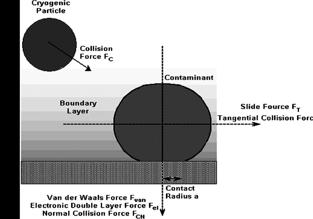
25 Van der Waals Force Particle Adhesion Omni-present, regardless whether they have dipoles Electrostatic forces Effect of ph and ionic strength on zeta potentials Capillary condensation Contact angles Measurement AFM Zeta potential
26 The Capillary and van der Waals force vs particle size Silica and alumina particles on a flat surface
27 SC-2 Dissolve and remove alkali residues and any residual trace metals or metal hydroxides Au, Ag Al(OH) 3, FeOH, Mg(OH) 2, or Zn(OH) 2 Dissolved metal ions form metal complexes Prevents replating from solution Does not etch Si or SiO 2 No surfactant activity or capability to remove particle Temperature control is more forgiving
28 Improvements Introduce a 10 second 1:50 diluted HF dip Between SC-1 and SC-2 Re-expose the Si surface for the SC-2 step Use fused silica vessels instead of Pyrex Eliminate leached glass components (e.g. sodium) Replacement of SC-2 with very dilute, room temperature HCl All metals except Ag and Au are readily soluble in dilute HCl, no need for oxidative desorption Au and Ag contaminants are no longer present in high-purity process chemicals
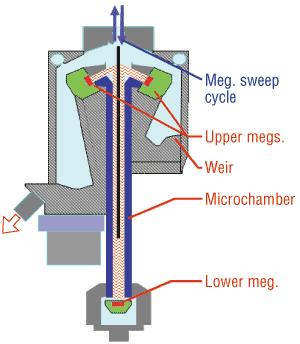
29 RCA Megasonic Cleaning System Megasonic treatment in SC-1 bath Allows substantial reduction in solution temperature Megasonic in rinsing of wafers Much more efficient than immersion tank processing
30 Megasonic Cleaning Ultrasonic energy with frequencies near 1 MHz Can be combined with other liquid cleaning solutions SC1 and SC2 Small acoustic boundary layer. small particle substrate bonding film S8 Acoustic boundary layer without magasonics small particle substrate bonding film S8 Acoustic boundary layer with magasonics A.A. Busnaina & F. Dai, Megasonic Cleaning Semiconductor International, August, 1997

31 Megasonic/Ultrasonic Transducers Piezoelectric transducers ceramic lead and zircon titanite (PZT)

32 Acoustic Streaming Eckart-type acoustic streaming
33 Magasonic Cleaning (II) Particle removal efficiency (PRE) Optimal megasonic power ( W) Optimal cleaning temperature (28-35 C) Optimal cleaning time (12-15 min) Redeposition


34 Dilemma between cleaning power and structure damage High particle removal efficiency (PRE) No substrate damage Low substrate film loss
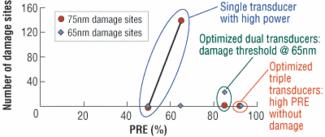
35 Dual-Transducer Megasonic Cleaning
36 Particle Removal Adopted by IC manufacturing RCA cleaning Brush scrubbing Megasonic cleaning In development Laser shock wave Supercritical CO 2 cleaning

37 Cryogenic Cleaning
38 Cryogenic Aerosol Cleaning Dry, non-aqueous, surface conditioning and cleaning method Contaminant removal is primarily by physical momentum transfer Does not etch or oxidize surface films CO 2, N 2, and Ar/N 2 cryoaerosols Particle removals in FEOL transistor gates or high aspect ratio patterns in the BEOL. Has been used in MEMS, read/write magnetic moemory heads, photomasks, compound semiconductor devices.


39 Equipment Waferclean 3600 manufactured by Eco-Snow Systems. The left-hand side image shows the inside of the process chamber of an ANTARES CX cleaning system. The right-side hand image depicts the flow pattern and particle transport path during cleaning. Courtesy of FSI International.
40 Nozzle-based cleaning technology Pressurized gas spray, pulsed liquid jet spray

41 Plasma source for rapid photoresist stripping Courtesy of Axcelis Technologies
42 Brushless post oxide CMP cleaning HF:HCl (1:2:200) for 5 24 C; Rinse with Ozone SC1 (1:2:30) for 6 70 C with megasonics Rinse with megasonics HF:HCl (1:2:200) for 5 24 C; Ozonated rinse, dry
MEGASONIC CLEANING OF WAFERS IN ELECTROLYTE SOLUTIONS: POSSIBLE ROLE OF ELECTRO-ACOUSTIC AND CAVITATION EFFECTS. The University of Arizona, Tucson
 MEGASONIC CLEANING OF WAFERS IN ELECTROLYTE SOLUTIONS: POSSIBLE ROLE OF ELECTRO-ACOUSTIC AND CAVITATION EFFECTS Manish Keswani 1, Srini Raghavan 1, Pierre Deymier 1 and Steven Verhaverbeke 2 1 The University
Pattern Transfer- photolithography
 Pattern Transfer- photolithography DUV : EUV : 13 nm 248 (KrF), 193 (ArF), 157 (F 2 )nm H line: 400 nm I line: 365 nm G line: 436 nm Wavelength (nm) High pressure Hg arc lamp emission Ref: Campbell: 7
PARTICLE ADHESION AND REMOVAL IN POST-CMP APPLICATIONS
 PARTICLE ADHESION AND REMOVAL IN POST-CMP APPLICATIONS George Adams, Ahmed A. Busnaina and Sinan Muftu the oratory Mechanical, Industrial, and Manufacturing Eng. Department Northeastern University, Boston,
Direct Measurement of Metallic Impurities in 20% Ammonium Hydroxide by 7700s/7900 ICP-MS
 Direct Measurement of Metallic Impurities in 20% Ammonium Hydroxide by 7700s/7900 ICP-MS Application Note Semiconductor Authors Junichi Takahashi Agilent Technologies Tokyo, Japan Abstract Ammonium hydroxide
The Removal of Nanoparticles from Nanotrenches Using Megasonics
 NSF Center for Micro and Nanoscale Contamination Control The Removal of Nanoparticles from Nanotrenches Using Megasonics Pegah Karimi 1, Tae Hoon Kim 1, Ahmed A. Busnaina 1 and Jin Goo Park 2 1 NSF Center
Figure 1: Graphene release, transfer and stacking processes. The graphene stacking began with CVD
 Supplementary figure 1 Graphene Growth and Transfer Graphene PMMA FeCl 3 DI water Copper foil CVD growth Back side etch PMMA coating Copper etch in 0.25M FeCl 3 DI water rinse 1 st transfer DI water 1:10
Removal of Cu Impurities on a Si Substrate by Using (H 2 O 2 +HF) and (UV/O 3 +HF)
 and (UV/O 3 +HF)") Journal of the Korean Physical Society, Vol. 33, No. 5, November 1998, pp. 579 583 Removal of Cu Impurities on a Si Substrate by Using (H 2 O 2 +HF) and (UV/O 3 +HF) Baikil Choi and Hyeongtag Jeon School
Journal of the Korean Physical Society, Vol. 33, No. 5, November 1998, pp. 579 583 Removal of Cu Impurities on a Si Substrate by Using (H 2 O 2 +HF) and (UV/O 3 +HF) Baikil Choi and Hyeongtag Jeon School
Regents of the University of California
 Deep Reactive-Ion Etching (DRIE) DRIE Issues: Etch Rate Variance The Bosch process: Inductively-coupled plasma Etch Rate: 1.5-4 μm/min Two main cycles in the etch: Etch cycle (5-15 s): SF 6 (SF x+ ) etches
MS482 Materials Characterization ( 재료분석 ) Lecture Note 12: Summary. Byungha Shin Dept. of MSE, KAIST
 Lecture Note 12: Summary. Byungha Shin Dept. of MSE, KAIST") 2015 Fall Semester MS482 Materials Characterization ( 재료분석 ) Lecture Note 12: Summary Byungha Shin Dept. of MSE, KAIST 1 Course Information Syllabus 1. Overview of various characterization techniques (1
2015 Fall Semester MS482 Materials Characterization ( 재료분석 ) Lecture Note 12: Summary Byungha Shin Dept. of MSE, KAIST 1 Course Information Syllabus 1. Overview of various characterization techniques (1
EE 527 MICROFABRICATION. Lecture 25 Tai-Chang Chen University of Washington
 EE 527 MICROFABRICATION Lecture 25 Tai-Chang Chen University of Washington ION MILLING SYSTEM Kaufmann source Use e-beam to strike plasma A magnetic field applied to increase ion density Drawback Low etch
Fabrication Technology, Part I
 EEL5225: Principles of MEMS Transducers (Fall 2004) Fabrication Technology, Part I Agenda: Microfabrication Overview Basic semiconductor devices Materials Key processes Oxidation Thin-film Deposition Reading:
EE C245 ME C218 Introduction to MEMS Design Fall 2007
 EE C245 ME C218 Introduction to MEMS Design Fall 2007 Prof. Clark T.-C. Nguyen Dept. of Electrical Engineering & Computer Sciences University of California at Berkeley Berkeley, CA 94720 Lecture 12: Mechanics
Dry Etching Zheng Yang ERF 3017, MW 5:15-6:00 pm
 Dry Etching Zheng Yang ERF 3017, email: yangzhen@uic.edu, MW 5:15-6:00 pm Page 1 Page 2 Dry Etching Why dry etching? - WE is limited to pattern sizes above 3mm - WE is isotropic causing underetching -
CVD: General considerations.
 CVD: General considerations. PVD: Move material from bulk to thin film form. Limited primarily to metals or simple materials. Limited by thermal stability/vapor pressure considerations. Typically requires
ETCHING Chapter 10. Mask. Photoresist
 ETCHING Chapter 10 Mask Light Deposited Substrate Photoresist Etch mask deposition Photoresist application Exposure Development Etching Resist removal Etching of thin films and sometimes the silicon substrate
NANO AND MICROSCALE PARTICLE REMOVAL
 NANO AND MICROSCALE PARTICLE REMOVAL Ahmed A. Busnaina William Lincoln Smith Professor and Director of the oratory Northeastern University, Boston, MA 2115-5 OUTLINE Goals and Objectives Approach Preliminary
DEPOSITION OF THIN TiO 2 FILMS BY DC MAGNETRON SPUTTERING METHOD
 Chapter 4 DEPOSITION OF THIN TiO 2 FILMS BY DC MAGNETRON SPUTTERING METHOD 4.1 INTRODUCTION Sputter deposition process is another old technique being used in modern semiconductor industries. Sputtering
Etching Issues - Anisotropy. Dry Etching. Dry Etching Overview. Etching Issues - Selectivity
 Etching Issues - Anisotropy Dry Etching Dr. Bruce K. Gale Fundamentals of Micromachining BIOEN 6421 EL EN 5221 and 6221 ME EN 5960 and 6960 Isotropic etchants etch at the same rate in every direction mask
Evaluation of Cleaning Methods for Multilayer Diffraction Gratings
 Evaluation of Cleaning Methods for Multilayer Diffraction Gratings Introduction Multilayer dielectric (MLD) diffraction gratings are essential components for the OMEGA EP short-pulse, high-energy laser
Wet and Dry Etching. Theory
 Wet and Dry Etching Theory 1. Introduction Etching techniques are commonly used in the fabrication processes of semiconductor devices to remove selected layers for the purposes of pattern transfer, wafer
Sample Analysis Design. Solution Mode
 Sample Analysis Design Solution Mode Step I Sample preparation The quality of your data will only be as good as the quality of your sample i.e. did you adequately prepare your sample in the clean lab?
Introduction to Photolithography
 http://www.ichaus.de/news/72 Introduction to Photolithography Photolithography The following slides present an outline of the process by which integrated circuits are made, of which photolithography is
4FNJDPOEVDUPS 'BCSJDBUJPO &UDI
 2010.5.4 1 Major Fabrication Steps in CMOS Process Flow UV light oxygen Silicon dioxide Silicon substrate Oxidation (Field oxide) photoresist Photoresist Coating Mask exposed photoresist Mask-Wafer Exposed
SPCC Department of Bio-Nano Technology and 2 Materials Science and Chemical Engineering, Hanyang University, Ansan, 15588, Republic of Korea.
 SPCC 2018 Hanyang University NEMPL Jin-Goo Park 1,2 *, Jung-Hwan Lee a, In-chan Choi 1, Hyun-Tae Kim 1, Lieve Teugels 3, and Tae-Gon Kim 3 1 Department of Bio-Nano Technology and 2 Materials Science and
Section 3: Etching. Jaeger Chapter 2 Reader
 Section 3: Etching Jaeger Chapter 2 Reader Etch rate Etch Process - Figures of Merit Etch rate uniformity Selectivity Anisotropy d m Bias and anisotropy etching mask h f substrate d f d m substrate d f
Device Fabrication: Etch
 Device Fabrication: Etch 1 Objectives Upon finishing this course, you should able to: Familiar with etch terminology Compare wet and dry etch processes processing and list the main dry etch etchants Become
Aspects of Single Wafer Cleans Processing and Tools
 Aspects of Single Wafer Cleans Processing and Tools Steven Verhaverbeke, Santa Clara, CA Date: June 16th, 2011 Contents 2 Generalities on Particles Generalities on particles in a chamber environment gas
Post Tungsten CMP Cleaner Development with Improved Organic and Particle Residue Removal on Silicon Nitride and Excellent Tungsten Compatibility
 Post Tungsten CMP Cleaner Development with Improved Organic and Particle Residue Removal on Silicon Nitride and Excellent Tungsten Compatibility Ching-Hsun Chao, Chi Yen, Ping Hsu, Eugene Lee, Paul Bernatis
What type of samples are common? Time spent on different operations during LC analyses. Number of samples? Aims. Sources of error. Sample preparation
 What type of samples are common? Sample preparation 1 2 Number of samples? Time spent on different operations during LC analyses 3 4 Sources of error Aims Sample has to be representative Sample has to
Determination of Impurities in Silica Wafers with the NexION 300S/350S ICP-MS
 APPLICATION NOTE ICP - Mass Spectrometry Author Kenneth Ong PerkinElmer, Inc. Singapore Determination of Impurities in Silica Wafers with the NexION 300S/350S ICP-MS Introduction The control of impurity
Sampling. Information is helpful in implementing control measures for reducing pollutant concentration to acceptable levels
 Types of pollutant sampling and measurement: Air quality monitoring: Sampling and measurement of air pollutants generally known, as air quality monitoring. It is an integral component of any air pollution
Experiment 1: Thin Layer Chromatography
 Experiment 1: Thin Layer Chromatography Part A: understanding R f values Part B: R f values & solvent polarity Part C: R f values & compound functionality Part D: identification of commercial food dye
A Novel Approach to the Layer Number-Controlled and Grain Size- Controlled Growth of High Quality Graphene for Nanoelectronics
 Supporting Information A Novel Approach to the Layer Number-Controlled and Grain Size- Controlled Growth of High Quality Graphene for Nanoelectronics Tej B. Limbu 1,2, Jean C. Hernández 3, Frank Mendoza
Two-Dimensional (C 4 H 9 NH 3 ) 2 PbBr 4 Perovskite Crystals for. High-Performance Photodetector. Supporting Information for
 2 PbBr 4 Perovskite Crystals for. High-Performance Photodetector. Supporting Information for") Supporting Information for Two-Dimensional (C 4 H 9 NH 3 ) 2 PbBr 4 Perovskite Crystals for High-Performance Photodetector Zhenjun Tan,,ǁ, Yue Wu,ǁ, Hao Hong, Jianbo Yin, Jincan Zhang,, Li Lin, Mingzhan
Supporting Information for Two-Dimensional (C 4 H 9 NH 3 ) 2 PbBr 4 Perovskite Crystals for High-Performance Photodetector Zhenjun Tan,,ǁ, Yue Wu,ǁ, Hao Hong, Jianbo Yin, Jincan Zhang,, Li Lin, Mingzhan
ICP-MS Analysis of Bulk & Process Chemicals for Semiconductor Processes. Ann O Connell Chemical Analysis Eng Intel Corporation
 ICPMS Analysis of Bulk & Process Chemicals for Semiconductor Processes Ann O Connell Chemical Analysis Eng Intel Corporation 1 Overview of Presentation Impact of Trace Metal contamination on Semiconductor
CHAPTER 3. FABRICATION TECHNOLOGIES OF CdSe/ZnS / Au NANOPARTICLES AND NANODEVICES. 3.1 THE SYNTHESIS OF Citrate-Capped Au NANOPARTICLES
 CHAPTER 3 FABRICATION TECHNOLOGIES OF CdSe/ZnS / Au NANOPARTICLES AND NANODEVICES 3.1 THE SYNTHESIS OF Citrate-Capped Au NANOPARTICLES Au NPs with ~ 15 nm were prepared by citrate reduction of HAuCl 4
CHAPTER 6: Etching. Chapter 6 1
 Chapter 6 1 CHAPTER 6: Etching Different etching processes are selected depending upon the particular material to be removed. As shown in Figure 6.1, wet chemical processes result in isotropic etching
Photolithography 光刻 Part II: Photoresists
 微纳光电子材料与器件工艺原理 Photolithography 光刻 Part II: Photoresists Xing Sheng 盛兴 Department of Electronic Engineering Tsinghua University xingsheng@tsinghua.edu.cn 1 Photolithography 光刻胶 负胶 正胶 4 Photolithography
EE 527 MICROFABRICATION. Lecture 24 Tai-Chang Chen University of Washington
 EE 527 MICROFABRICATION Lecture 24 Tai-Chang Chen University of Washington EDP ETCHING OF SILICON - 1 Ethylene Diamine Pyrocatechol Anisotropy: (100):(111) ~ 35:1 EDP is very corrosive, very carcinogenic,
Microorganisms. Dissolved inorganics. Native vs. Introduced; Oligotrophic vs. Eutrophic Millions to billions per ml or g Complex consortia
 1 Microorganisms Native vs. Introduced; Oligotrophic vs. Eutrophic Millions to billions per ml or g Complex consortia Species makeup: f(t, O 2, ph, nutrients, etc.) Indicators & pathogens Dissolved inorganics
Lecture 0: Introduction
 Lecture 0: Introduction Introduction q Integrated circuits: many transistors on one chip q Very Large Scale Integration (VLSI): bucketloads! q Complementary Metal Oxide Semiconductor Fast, cheap, low power
The goal of this project is to enhance the power density and lowtemperature efficiency of solid oxide fuel cells (SOFC) manufactured by atomic layer
 manufactured by atomic layer") Stanford University Michael Shandalov1, Shriram Ramanathan2, Changhyun Ko2 and Paul McIntyre1 1Department of Materials Science and Engineering, Stanford University 2Division of Engineering and Applied
Stanford University Michael Shandalov1, Shriram Ramanathan2, Changhyun Ko2 and Paul McIntyre1 1Department of Materials Science and Engineering, Stanford University 2Division of Engineering and Applied
EXPERIMENT 7 Reaction Stoichiometry and Percent Yield
 EXPERIMENT 7 Reaction Stoichiometry and Percent Yield INTRODUCTION Stoichiometry calculations are about calculating the amounts of substances that react and form in a chemical reaction. The word stoichiometry
Hybrid Wafer Level Bonding for 3D IC
 Hybrid Wafer Level Bonding for 3D IC An Equipment Perspective Markus Wimplinger, Corporate Technology Development & IP Director History & Roadmap - BSI CIS Devices???? 2013 2 nd Generation 3D BSI CIS with
Supplementary Figure 1 Detailed illustration on the fabrication process of templatestripped
 Supplementary Figure 1 Detailed illustration on the fabrication process of templatestripped gold substrate. (a) Spin coating of hydrogen silsesquioxane (HSQ) resist onto the silicon substrate with a thickness
UNIVERSITY OF CALIFORNIA College of Engineering Department of Electrical Engineering and Computer Sciences. Fall Exam 1
 UNIVERSITY OF CALIFORNIA College of Engineering Department of Electrical Engineering and Computer Sciences EECS 143 Fall 2008 Exam 1 Professor Ali Javey Answer Key Name: SID: 1337 Closed book. One sheet
CEINT/NIST PROTOCOL REPORTING GUIDELINES FOR THE PREPARATION OF AQUEOUS NANOPARTICLE DISPERSIONS FROM DRY MATERIALS. Ver. 2.0
 CEINT/NIST PROTOCOL REPORTING GUIDELINES FOR THE PREPARATION OF AQUEOUS NANOPARTICLE DISPERSIONS FROM DRY MATERIALS Ver. 2.0 July 8, 2010 Protocol Contributors: J. S. Taurozzi 1, V. A. Hackley 1, M. R.
Photolithography Overview 9/29/03 Brainerd/photoclass/ECE580/Overvie w/overview
 http://www.intel.com/research/silicon/mooreslaw.htm 1 Moore s law only holds due to photolithography advancements in reducing linewidths 2 All processing to create electric components and circuits rely
Fall 2011 CHEM Test 4, Form A
 Fall 2011 CHEM 1110.40413 Test 4, Form A Part I. Multiple Choice: Clearly circle the best answer. (60 pts) Name: 1. The common constituent in all acid solutions is A) H 2 SO 4 B) H 2 C) H + D) OH 2. Which
Introduction to Nanotechnology Chapter 5 Carbon Nanostructures Lecture 1
 Introduction to Nanotechnology Chapter 5 Carbon Nanostructures Lecture 1 ChiiDong Chen Institute of Physics, Academia Sinica chiidong@phys.sinica.edu.tw 02 27896766 Carbon contains 6 electrons: (1s) 2,
Fast Bonding of Substrates for the Formation of Microfluidic Channels at Room Temperature
 Supplementary Material (ESI) for Lab on a Chip This journal is The Royal Society of Chemistry 2005 Supporting Information Fast Bonding of Substrates for the Formation of Microfluidic Channels at Room Temperature
Gold nanothorns macroporous silicon hybrid structure: a simple and ultrasensitive platform for SERS
 Supporting Information Gold nanothorns macroporous silicon hybrid structure: a simple and ultrasensitive platform for SERS Kamran Khajehpour,* a Tim Williams, b,c Laure Bourgeois b,d and Sam Adeloju a
Film Deposition Part 1
 1 Film Deposition Part 1 Chapter 11 : Semiconductor Manufacturing Technology by M. Quirk & J. Serda Spring Semester 2013 Saroj Kumar Patra Semidonductor Manufacturing Technology, Norwegian University of
XPS/UPS and EFM. Brent Gila. XPS/UPS Ryan Davies EFM Andy Gerger
 XPS/UPS and EFM Brent Gila XPS/UPS Ryan Davies EFM Andy Gerger XPS/ESCA X-ray photoelectron spectroscopy (XPS) also called Electron Spectroscopy for Chemical Analysis (ESCA) is a chemical surface analysis
SYNTHESIS OF INORGANIC MATERIALS AND NANOMATERIALS. Pr. Charles Kappenstein LACCO, Laboratoire de Catalyse en Chimie Organique, Poitiers, France
 SYNTHESIS OF INORGANIC MATERIALS AND NANOMATERIALS Pr. Charles Kappenstein LACCO, Laboratoire de Catalyse en Chimie Organique, Poitiers, France Outline IV - FORMATION OF SOLIDS FROM SOLUTIONS 1) Glass
Supplementary Figure 1. Temperature profile of self-seeding method for polymer single crystal preparation in dilute solution.
 Supplementary Figure 1. Temperature profile of self-seeding method for polymer single crystal preparation in dilute solution. Supplementary Figure 2. 1 H nuclear magnetic resonance (NMR) spectra (a) and
Name Period Date. Lab 10: Paper Chromatography
 Name Period Date Lab 10: Paper Chromatography Objectives Known and unknown solutions of the metal ions Fe +, Cu 2+ and Ni 2+ will be analyzed using paper chromatography. An unknown solution containing
EE C245 ME C218 Introduction to MEMS Design Fall 2007
 EE C245 ME C218 Introduction to MEMS Design Fall 2007 Prof. Clark T.-C. Nguyen Dept. of Electrical Engineering & Computer Sciences University of California at Berkeley Berkeley, CA 94720 Lecture 4: Film
Current State of Extraction Don t Be Deceived! Sharon F. Webb, Ph.D. Director of Quality Program
 Current State of Extraction Don t Be Deceived! Sharon F. Webb, Ph.D. Director of Quality Program Overview Factors Purpose of Dissolution Quality Objectives of Program Effectiveness of Dissolution Technique
Model 2300XP PSL & Process-Particle Wafer Deposition System
 Model 2300XP PSL & Process-Particle Wafer Deposition System Deposit PSL spheres on wafers to create NISTtraceable PSL size standards for - calibrating wafer inspection systems - providing fab-wide and
Evaluation of the plasmaless gaseous etching process
 Solid State Phenomena Vol. 134 (28) pp 7-1 Online available since 27/Nov/2 at www.scientific.net (28) Trans Tech Publications, Switzerland doi:1.428/www.scientific.net/ssp.134.7 Evaluation of the plasmaless
Basic Digestion Principles
 Basic Digestion Principles 1 From Samples to Solutions Direct Analytical Method Solid Sample Problems: Mech. Sample Preparation (Grinding, Sieving, Weighing, Pressing, Polishing,...) Solid Sample Autosampler
UHF-ECR Plasma Etching System for Dielectric Films of Next-generation Semiconductor Devices
 UHF-ECR Plasma Etching System for Dielectric Films of Next-generation Semiconductor Devices 1 UHF-ECR Plasma Etching System for Dielectric Films of Next-generation Semiconductor Devices Katsuya Watanabe
Lecture 7 Contact angle phenomena and wetting
 Lecture 7 Contact angle phenomena and Contact angle phenomena and wetting Young s equation Drop on the surface complete spreading Establishing finite contact angle γ cosθ = γ γ L S SL γ S γ > 0 partial
Reactive Ion Etching (RIE)
") Reactive Ion Etching (RIE) RF 13.56 ~ MHz plasma Parallel-Plate Reactor wafers Sputtering Plasma generates (1) Ions (2) Activated neutrals Enhance chemical reaction 1 2 Remote Plasma Reactors Plasma Sources
Reactive Ion Etching (RIE) RF 13.56 ~ MHz plasma Parallel-Plate Reactor wafers Sputtering Plasma generates (1) Ions (2) Activated neutrals Enhance chemical reaction 1 2 Remote Plasma Reactors Plasma Sources
Holographic Characterization of Agglomerates in CMP Slurries
 Holographic Characterization of Agglomerates in CMP Slurries Total Holographic Characterization (THC) Comparison of THC to other technologies Dynamic Light Scattering (DLS) Scanning Electron Microscopy
In Situ and Real-Time Metrology during Cleaning, Rinsing, and Drying of Microand Nano-Structures
 In Situ and Real-Time Metrology during Cleaning, Rinsing, and Drying of Microand Nano-Structures Jun Yan *, Davoud Zamani *, Bert Vermeire +, Farhang Shadman * * Chemical Engineering, University of Arizona
Supporting Information
 Supporting Information Assembly and Densification of Nanowire Arrays via Shrinkage Jaehoon Bang, Jonghyun Choi, Fan Xia, Sun Sang Kwon, Ali Ashraf, Won Il Park, and SungWoo Nam*,, Department of Mechanical
Organization of silica spherical particles into different shapes on silicon substrates
 Materials Science-Poland, Vol. 25, No. 3, 2007 Organization of silica spherical particles into different shapes on silicon substrates B. KORUSIEWICZ 1, K. MARUSZEWSKI 1,2* 1 Wrocław University of Technology,
Etching: Basic Terminology
 Lecture 7 Etching Etching: Basic Terminology Introduction : Etching of thin films and sometimes the silicon substrate are very common process steps. Usually selectivity, and directionality are the first
Plasma Surface Modification for Cleaning and Adhesion Ron Nickerson, Vice President AST Products, Inc. Billerica, MA
 Plasma Surface Modification for Cleaning and Adhesion Ron Nickerson, Vice President AST Products, Inc. Billerica, MA. 01821 978-663-7652 When manufacturers scramble to find processes of surface cleaning
(50 pts.) 26. (24 pts.) 27. (8 pts.) 28. (18 pts.) TOTAL (100 points)
 26. (24 pts.) 27. (8 pts.) 28. (18 pts.) TOTAL (100 points)") Moorpark College Chemistry 11 Spring 2011 Instructor: Professor Torres Examination #2: Section Two March 12, 2011 Name: (print) Name: (sign) Directions: Make sure your examination contains ELEVEN total
Moorpark College Chemistry 11 Spring 2011 Instructor: Professor Torres Examination #2: Section Two March 12, 2011 Name: (print) Name: (sign) Directions: Make sure your examination contains ELEVEN total
CHAPTER 11: Intermolecular Forces, Liquids, and Solids. Are there any IDEAL GASES? The van der Waals equation corrects for deviations from ideality
 CHAPTER 11: Intermolecular Forces, Liquids, and Solids Are there any IDEAL GASES? The van der Waals equation corrects for deviations from ideality Does the KMT break down? Kinetic Molecular Theory 1. Gas
Self-study problems and questions Processing and Device Technology, FFF110/FYSD13
 Self-study problems and questions Processing and Device Technology, FFF110/FYSD13 Version 2016_01 In addition to the problems discussed at the seminars and at the lectures, you can use this set of problems
Industrial Applications of Ultrafast Lasers: From Photomask Repair to Device Physics
 Industrial Applications of Ultrafast Lasers: From Photomask Repair to Device Physics Richard Haight IBM TJ Watson Research Center PO Box 218 Yorktown Hts., NY 10598 Collaborators Al Wagner Pete Longo Daeyoung
Graphene The Search For Two Dimensions. Christopher Scott Friedline Arizona State University
 Graphene The Search For Two Dimensions Christopher Scott Friedline Arizona State University What Is Graphene? Single atomic layer of graphite arranged in a honeycomb crystal lattice Consists of sp 2 -bonded
Metal Deposition. Filament Evaporation E-beam Evaporation Sputter Deposition
 Metal Deposition Filament Evaporation E-beam Evaporation Sputter Deposition 1 Filament evaporation metals are raised to their melting point by resistive heating under vacuum metal pellets are placed on
Auger Electron Spectroscopy (AES)
") 1. Introduction Auger Electron Spectroscopy (AES) Silvia Natividad, Gabriel Gonzalez and Arena Holguin Auger Electron Spectroscopy (Auger spectroscopy or AES) was developed in the late 1960's, deriving
1. Introduction Auger Electron Spectroscopy (AES) Silvia Natividad, Gabriel Gonzalez and Arena Holguin Auger Electron Spectroscopy (Auger spectroscopy or AES) was developed in the late 1960's, deriving
DIFFERENT TYPES OF INTEMOLECULAR FORCES INTERMOLECULAR FORCES
 DIFFERENT TYPES OF INTEMOLECULAR FORCES Do all the exercises in your studyguide COMPARISON OF THE THREE PHASES OF MATTER. Matter is anything that occupy space and has mass. There are three states of matter:
Water and Aqueous Systems
 Water and Aqueous Systems The Water Molecule: a Review Water is a simple tri-atomic molecule, H 2 O Each O-H bond is highly polar, because of the high electronegativity of the oxygen (N, O, F, and Cl have
Equipment Innovation Team, Memory Fab. Center, Samsung Electronics Co. Ltd. San#16, Banwol, Taean, Hwansung, Kyungki, , Republic of Korea
 Solid State Phenomena Vols. 103-104 (2005) pp 63-66 Online available since 2005/Apr/01 at www.scientific.net (2005) Trans Tech Publications, Switzerland doi:10.4028/www.scientific.net/ssp.103-104.63 Development
Characterization of Post-etch Residue Clean By Chemical Bonding Transformation Mapping
 Characterization of Post-etch Residue Clean By Chemical Bonding Transformation Mapping Muthappan Asokan, Oliver Chyan*, Interfacial Electrochemistry and Materials Research Lab, University of North Texas
Case Study of Electronic Materials Packaging with Poor Metal Adhesion and the Process for Performing Root Cause Failure Analysis
 Case Study of Electronic Materials Packaging with Poor Metal Adhesion and the Process for Performing Root Cause Failure Analysis Dr. E. A. Leone BACKGRUND ne trend in the electronic packaging industry
SUPPLEMENTARY INFORMATION
 doi:.38/nature09979 I. Graphene material growth and transistor fabrication Top-gated graphene RF transistors were fabricated based on chemical vapor deposition (CVD) grown graphene on copper (Cu). Cu foil
MICROCHIP MANUFACTURING by S. Wolf
 by S. Wolf Chapter 5: GASES, LIQUID-CHEMICALS, & ULTRAPURE-WATER FOR ULSI Chapter 5: Gases, Liquid-Chemicals & CHAPTER CONTENTS Basic Properties of Materials Temperature Thermal Expasio of Materials Liquid
Fabrication of ordered array at a nanoscopic level: context
 Fabrication of ordered array at a nanoscopic level: context Top-down method Bottom-up method Classical lithography techniques Fast processes Size limitations it ti E-beam techniques Small sizes Slow processes
Supplementary Information. Rapid Stencil Mask Fabrication Enabled One-Step. Polymer-Free Graphene Patterning and Direct
 Supplementary Information Rapid Stencil Mask Fabrication Enabled One-Step Polymer-Free Graphene Patterning and Direct Transfer for Flexible Graphene Devices Keong Yong 1,, Ali Ashraf 1,, Pilgyu Kang 1,
LECTURE 5 SUMMARY OF KEY IDEAS
 LECTURE 5 SUMMARY OF KEY IDEAS Etching is a processing step following lithography: it transfers a circuit image from the photoresist to materials form which devices are made or to hard masking or sacrificial
Plasma Deposition (Overview) Lecture 1
 Lecture 1") Plasma Deposition (Overview) Lecture 1 Material Processes Plasma Processing Plasma-assisted Deposition Implantation Surface Modification Development of Plasma-based processing Microelectronics needs (fabrication
Plasma Deposition (Overview) Lecture 1 Material Processes Plasma Processing Plasma-assisted Deposition Implantation Surface Modification Development of Plasma-based processing Microelectronics needs (fabrication
Supporting information
 Supporting information Influence of electrolyte composition on liquid-gated carbon-nanotube and graphene transistors By: Iddo Heller, Sohail Chatoor, Jaan Männik, Marcel A. G. Zevenbergen, Cees Dekker,
Techniques for the Analysis of Organic Chemicals by Inductively Coupled Plasma Mass Spectrometry (ICP-MS)
") Techniques for the Analysis of Organic Chemicals by Inductively Coupled Plasma Mass Spectrometry (ICP-MS) Petrochemical Authors Ed McCurdy & Don Potter Agilent Technologies Ltd. Lakeside Cheadle Royal
Techniques for the Analysis of Organic Chemicals by Inductively Coupled Plasma Mass Spectrometry (ICP-MS) Petrochemical Authors Ed McCurdy & Don Potter Agilent Technologies Ltd. Lakeside Cheadle Royal
Large Scale Direct Synthesis of Graphene on Sapphire and Transfer-free Device Fabrication
 Supplementary Information Large Scale Direct Synthesis of Graphene on Sapphire and Transfer-free Device Fabrication Hyun Jae Song a, Minhyeok Son a, Chibeom Park a, Hyunseob Lim a, Mark P. Levendorf b,
Direct Analysis of Photoresist Using Inductively Coupled Plasma Mass Spectrometry (ICP-MS) Application
 Application") Direct Analysis of Photoresist Using Inductively Coupled Plasma Mass Spectrometry (ICP-MS) Application Semiconductor Author Junichi Takahashi Koichi Yono Agilent Technologies, Inc. 9-1, Takakura-Cho, Hachioji-Shi,
Direct Analysis of Photoresist Using Inductively Coupled Plasma Mass Spectrometry (ICP-MS) Application Semiconductor Author Junichi Takahashi Koichi Yono Agilent Technologies, Inc. 9-1, Takakura-Cho, Hachioji-Shi,
PRINCIPLE OF ICP- AES
 INTRODUCTION Non- flame atomic emission techniques, which use electrothermal means to atomize and excite the analyte, include inductively coupled plasma and arc spark. It has been 30 years since Inductively
Application. Determination of Trace Metal Impurities in Semiconductor-Grade Hydrofluoric Acid. Authors. Introduction. Abstract.
 Determination of Trace Metal Impurities in Semiconductor-Grade Hydrofluoric Acid Application Semiconductor Authors Abe G. Gutiérrez Elemental Scientific 2440 Cuming St Omaha, NE 68131 USA abe@icpms.com
Chapter 11 Properties of Solutions
 Chapter 11 Properties of Solutions Solutions Homogeneous mixtures of two or more substances Composition is uniform throughout the sample No chemical reaction between the components of the mixture Solvents
Lecture 150 Basic IC Processes (10/10/01) Page ECE Analog Integrated Circuits and Systems P.E. Allen
 Page ECE Analog Integrated Circuits and Systems P.E. Allen") Lecture 150 Basic IC Processes (10/10/01) Page 1501 LECTURE 150 BASIC IC PROCESSES (READING: TextSec. 2.2) INTRODUCTION Objective The objective of this presentation is: 1.) Introduce the fabrication of
Lecture 150 Basic IC Processes (10/10/01) Page 1501 LECTURE 150 BASIC IC PROCESSES (READING: TextSec. 2.2) INTRODUCTION Objective The objective of this presentation is: 1.) Introduce the fabrication of
States of Matter. Solid. Liquid. Gas Plasma
 States of Matter Solid Liquid Gas Plasma Your turn Write four (4) examples each for Solids, Liquids, and Gases. Try to use examples you have personally been in contact with How they relate Based on what
Unit 6 Solids, Liquids and Solutions
 Unit 6 Solids, Liquids and Solutions 12-1 Liquids I. Properties of Liquids and the Kinetic Molecular Theory A. Fluids 1. Substances that can flow and therefore take the shape of their container B. Relative
NSF Center for Micro and Nanoscale Contamination Control
 NSF Center for Micro and Nanoscale Contamination Control Research Focus at the NSF Center for Nano and Microcontamination Control Ahmed Busnaina W. L. Smith Professor and Director NSF Center for Microcontamination