YIA: Interaction of Radiation with Graphene-based Nanomaterials for Sensing Fissile Materials (Grant # HDTRA )
|
|
|
- Clement Martin
- 6 years ago
- Views:
Transcription
1 YIA: Interaction of Radiation with Graphene-based Nanomaterials for Sensing Fissile Materials (Grant # HDTRA ) Yong P. Chen (yongchen@purdue.edu), Purdue University DTRA Technical Review 10/21/2009


")


2 Introduction & Background Radiation detection has been very closely coupled with advances in semiconductors.. How Can graphene do it (well)? The gravest danger we face---nuclear terrorism /16/08 at Purdue University (Summit on Confronting New Threats) And the biggest threat that we face right now is not a nuclear missile coming over the skies. It's in a suitcase /28/2008 during 1 st Presidential debate 2
![Radiation Detection SNM/FM Radiation Sensing --- some state of art: High Resolution is Desirable HPGE (High Purity Ge) [charge collection]](/docs-images/74/70357332/images/3-1.jpg "Superconductor TES (Transition Edge Sensor) [NOT charge collection; use a sharp feature] Can we have a sharp feature @ ~ room T that couples to")
3 Radiation Detection SNM/FM Radiation Sensing --- some state of art: High Resolution is Desirable HPGE (High Purity Ge) [charge collection] Superconductor TES (Transition Edge Sensor) [NOT charge collection; use a sharp feature] Can we have a sharp ~ room T that couples to radiation(effect) 3
")
materials New wonder")
")
 Amazing Thermal properties")
 Electrons in")

![graphene] High conductivity/mobility (>10X Si @](/docs-images/74/70357332/images/4-6.jpg "room T) Low (electronic) noise Tunable (electr.")
4 What is Graphene Usual solid graphene papers in 2008 (electrically isolated) discovered in 2004 Building block of many carbon (nano)materials New wonder semiconductor/semimetal Amazing Electrical Properties ( post Si electronics/ Moore ) Amazing Mechanical Properties --- highest strength (~CNT) Amazing Thermal properties highest thermal conductivity Easy to make and work with (2D planar fabrication) Electrons in graphene E v F pv F ~ 1 10 kv 6 m/s Dirac equation Chiral massless fermions [QED/QCD in graphene] High conductivity/mobility (>10X room T) Low (electronic) noise Tunable (electr.) properties Exposed to environment --- excellent sensor mat. F 4
 Dirac pt (<n>=0) p n Finite R (quantum R) Low noise")
![High mobility (can ballistic) High speed [THz] High sensitivity [de/e<10-3 ]](/docs-images/74/70357332/images/5-3.jpg "Bandgap eng possible all these even at 300K the sharp feature F.")
5 Sharp Electric Field Effect in Graphene GFET insulator graphene V gate semiconductor (doped) Dirac pt (<n>=0) p n Finite R (quantum R) Low noise High mobility (can ballistic) High speed [THz] High sensitivity [de/e<10-3 ] Bandgap eng possible all these even at 300K the sharp feature F. Schedin et al
6 GFET for radiation sensing Graphene resistance R (kohm) R (kohm) How well can GFET detect radiation [rare events] -3x Electric Field (V/m) -3x Electric Field (V/m) Sensitivity/energy resolution? V gate insulator semiconductor graphene Small E field (undoped/~insulating) V gate insulator semiconductor (conductive) graphene Large E field Graphene a highly sensitive to detect local Efield-chage [single molecule sensitivity] Vgate tunable - sensitivity and resolution NOT relying on collecting/drifting ionizded charges; appearance of ionized charges changes electric field sensing Efield intrinsically faster than sensing drfited/collected charges can work with variety of absorber substrates for gamma/neutron interaction; thin insulator layer 6

 [Baladin 09] J-H.")
7 Possible alternative schemes: Physico/Chemical Change due to radiation Stolyarova et al 2009 Also: electron-beam irradiation creates defects (see later) [Baladin 09] J-H.Chen et al 2009 (Ne+/He+ irradiation) 7


8 Graphene Composite+ for Radiation Sensing Stankovich et al 06 Graphene composite: Graphene sheets dispersed in polymer matrix bottom up approach (graphene composite+) : semiconductor/absorber nanoparticles How would radiation interacts with such material How would composite respond to radiation in a detectable way? 8
9 Research Summary Objective: 1) Understand the basic science about how ionizing radiation (gamma rays, neutrons) and associated charged particles interact with nano-materials/structures based on graphene, which has shown extreme sensitivity to local environmental perturbations; 2) Develop scientific foundation that may lead to graphene based radiation sensors with sensitivity & energy resolution in par or exceeding HPGe sensors and operating at close to room T for long distance fissile material detection. Approach: Two material systems: Graphene on radiation absorbing (semiconductor) substrates [Yr1 focus] and Graphene composite with radiation absorbing fillings [Yr2 focus]. Electrical, Raman and microscopy measurements will be used to study both transient and accumulative radiation effects [gamma/neutrons]. Collaboration: Purdue (Nucl. Eng.; Applied Physics Lab); NWU (Materials Sci. [graphene composite]); U. Houston (ECE [large scale CVD graphene]); leverage from NSF/DHS-ARI Program (GFET) 9


10 Research Purdue Birck Nanotechnology Center (BNC) Applied Physics Laboratory Nuclear/Civil Engineering Physics 10
11 Preliminary Work and Related Technical Accomplishments V gate insulator semiconductor absorber graphene GFET based radiation sensor (eg. sharp change of resistivity due to change of electrical field caused by ionizing radiation) Graphene composite Modeling of radiation-material interaction; Modeling of possible radiation detection schemes using graphene-based sensors Fabricating/Developing/Characterizing suitable graphene-based materials and devices Proof of concept experiments with graphene field effect transistors: radiation responses; local electric field sensitivity Physico-chemical changes: studies of effects of charged-particles irradiation on graphene and GFET 11
12 Modeling: radiation-substrate (absorber) interaction MCNP and MCNP-Polimi modeling of interaction of ionizing radiation (gamma, neutrons) with absorber materials: various semiconductors (Si, Ge, InSb), polystyrene etc. Compton electron transport through substrate (CASINO) recently also started using Geant4 (collab. I. Jovanovic [Purdue Nucl E]) 12
13 Modeling: radiation-substrate (absorber) interaction Geant4 CASINO 13
 1.0 0.")

14 COMSOL Modeling: GFET response to radiation ionized charges Gabe Lopez et al., R (kohm) x Electric Field (V/m) V gate insulator semiconductor absorber graphene Simplified model with straight tracks --- good for neutrons? Ionized/conducting region 14

15 Detection schemes; Sensitivity and Energy Resolution radiation GFET absorber Also want large, high quality graphene to cover all generated charges Various possible detections schemes under investigation: remote detection FET (better for straight tracks/neutrons?) drift charges, but do not collect them use graphene (as effective low noise amplifier to read out the charges (for gammas?). 15


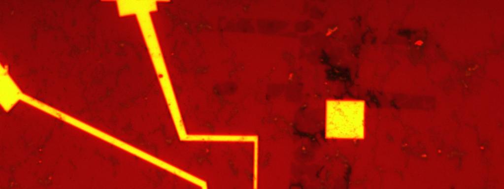
16 Material/Device Fabrication of Graphene and GFET exfoliation (scotch tape) Graphene on doped Si with 300 nm oxide E-beam lithography e - e - Lithography Nanodevices Develop PMMA Cr/Au evaporation Photo by Sambandamurthy Doped Si Lift off SiO 2 PMMA Cr/Au 16


")
/14 Quantum Hall Effect")
/10 (h/e 2 )/2 I.")
17 How to identify graphene light Ni et al nm Optical microscopy -- seeing is believing Raman Spectroscopy (also sensitive to defects in graphene) Many layers Gupta et al 2007 Resistance (ohms) 30x Rxx Rxy (h/e 2 )/14 Quantum Hall Effect (magnetoresistance) (h/e 2 )/6 (h/e 2 )/10 (h/e 2 )/2 I.Childres et al (see poster 3) Gate Voltage (V) 20 17
18 GFET Characterization S D (grounded) Semiconductor=Si Insulator=300nm SiO2 V gate insulator semiconductor (doped) graphene Want: high-mobilty graphene [sharp FET] 2.0 G 500x mv R (kohm) I DS Dirac 3 mv 2 mv mv -3x Electric Field (V/m) V GS
19 Large-scale Graphene Available by CVD 4-in graphene! Q. Yu (UH) Quantum Hall Effect h/2e 2 H. Cao et al


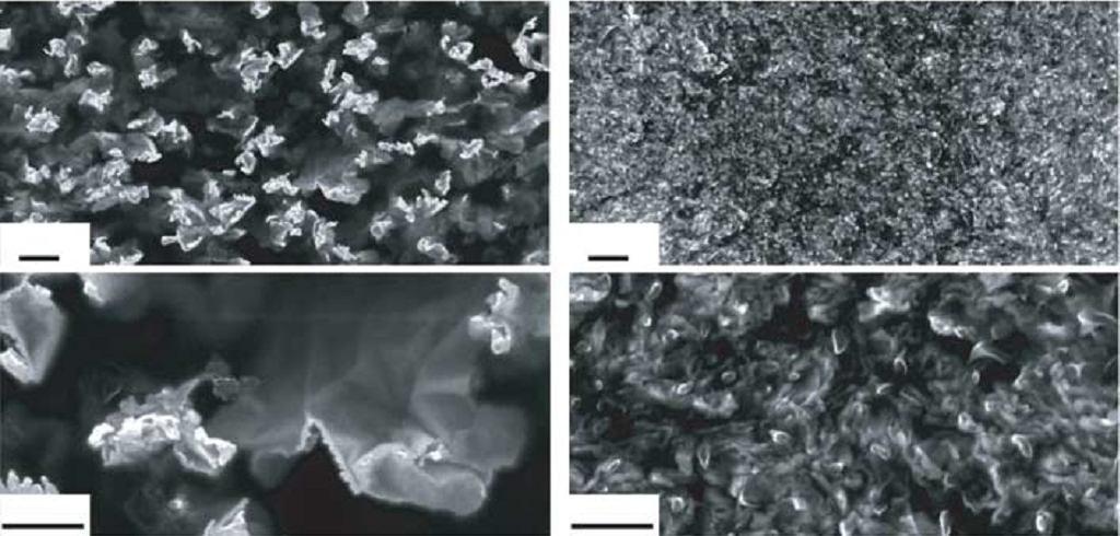
20 Other Graphene-based Materials [Work done by undergrads] Fabricating Graphene on Ge & other substrates Stephen (ECE-Y3) Caleb (NE-Y4) (w/t 30nm germanium oxide) Synthesizing Graphene Oxide & Graphene Composite Stankovich et al 06 Sarah (CheE-Y2) 20
![Proof of Concept: Photo-actuated GFET Radiation [this case, laser] chopper (doped) Also tried](/docs-images/74/70357332/images/21-0.jpg "photo-resistor similar to photodiode Also tried MOSFET G.Lopez et al.")
 0.10 0.08 0.06 0.04 0.")
21 Proof of Concept: Photo-actuated GFET Radiation [this case, laser] chopper (doped) Also tried photo-resistor similar to photodiode Also tried MOSFET G.Lopez et al. Experiments currently underway with undoped Si-substrate hospital X-ray source 82mC gamma source Voltage (volt) Photodiode Vds of GFET at 20HZ Vds of GFET at 100HZ Vds of GFET at Ids=10uA -40x time (sec) 21


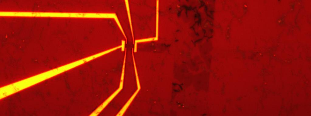
22 Local Field Effect: by Side Gate Graphene is sensitive to local electric field side gate J. Tian et al., 22

 Vbg = 13 V Location1 Location2 Location3-20 -10 0 10 20 V top")
 300x10 6 200 100 0-2x10⁻⁶ -1 0 1 2 Distance (m) Vbg = 16 V location1")
 Graphene SiO 2 p-type Si Apply I ds Read V ds Jalilian et al 09 unexpected scientific")
23 Local Electric Field Effect by AFM tip R(kohm) R (Kohm) m Vbg = 0V Location1 Location2 Location3 100 nm Vbg = 11V location1 location2 location V top gate (V) V top gate (V) R(Kohm) R (Kohm) back gate voltage (V) Vbg = 13 V Location1 Location2 Location V top gate (V) R (Kohm) R (Kohm) Electric feild (V/m) 300x x Distance (m) Vbg = 16 V location1 location2 location V top gate (V) Vbg=20V location1 location2 location V top gate (V) Graphene SiO 2 p-type Si Apply I ds Read V ds Jalilian et al 09 unexpected scientific discovery: charge inhomogeneity (puddles) near Dirac point V bg V tg
 also relevant for (long term) reliability of GFET radiation sensors 30keV")
 charges Raman spectra [cf also Baladin APL")
24 Charged-particles irradiation: e-beam effect of energetic charged particles (eg. electrons) also relevant for (long term) reliability of GFET radiation sensors 30keV electron beam I= 0.15nA; Time=5mins; Expose area: 50um x 50um Estimated dose: e-/nm 2 e- beam adds to graphene negative (n-) charges Raman spectra [cf also Baladin APL 09] (I.Childres et al) 24
 0 5 10 15 Gate Voltage (V) 20 0")
25 Charged-particles irradiation: O + ions Resistance (ohms) Before Exposure (4-terminal) s exposure (3-terminal) s exposure (3-terminal) Gate Voltage (V) Gate Voltage (V) Intensity (offset) D Raman spectra Increasing exposure O+ ions add to graphene positive (p+) charges Defect creation studied also by: Raman spectroscopy AFM (atomic force microscopy) time-dependent behavior I. Childres et al., in preparation These studies also relevant for rad-hard graphene electronics! O+ ions generated in a microwave plasma chamber Wavenumber (cm-1)
26 Presentations/Publications 10th International Conference on Applications of Nuclear Techniques (Crete, Greece June 2009) (I. Childres et al. on e- beam irradiated GFET) In preparation: IEEE NSS/MIC (Orlando 2009) on graphene radiation detector & modeling [accepted] Manuscript(s) on charged-particle irradiation effect Manuscript(s) on local gate/charge FET 26
 and associated charged particles interact with nano-materials/structures based on graphene, which has shown extreme sensitivity to local")
: Raman, AFM and electronic measurements of GFET and effect of charged particles (O+ ions and electron")
.")

27 YIA: Interaction of Radiation with Graphene-based Nanomaterials for Sensing Fissile Materials Compton electron transport Sharp field effect Physicochemical change Objectives/Metrics: We aim to elucidate how ionizing radiation (gamma rays, neutrons) and associated charged particles interact with nano-materials/structures based on graphene, which has shown extreme sensitivity to local environmental perturbations. Performer: Prof. Yong P. Chen, Purdue University Status: Program started in Fall 09 Accomplishments (Preliminary Results): Raman, AFM and electronic measurements of GFET and effect of charged particles (O+ ions and electron beams) on graphene Geant4/MCNP-CASINO & COMSOL modeling of gamma rays interaction with absorber and electrical field effect on graphene Description: This Young Investigator Award (YIA) program is funded under Topic Y-4: Sensing Fissile Materials at Long Range using Nano-Structured Detector Materials (Thrust 1). It will study the interaction of radiation with various nanomaterials based on graphene, whose exceptional properties may enable remote detection of fissile materials with great sensitivity. Electrical, Raman and microscopy measurements will be used to study transient and accumulative radiation effects. Key deliverables: Data on from experiments and simulations Regular reports Peer-reviewed journal publications Conference presentations and proceeding papers Graduate and undergraduate students trained in related areas Funding Profile: Current: FY10: $0.1M FY11: $0.1M Key Milestones: FY10: Understand the mechanisms of radiation interaction with graphene on semiconductor substrates and how the interaction changes graphene properties FY11:Understand the mechanisms of radiation interaction with graphene composites and how the interaction changes the composite material properties 27

: likely to require new mechanisms unexplored previously Nanostructured materials have great, largely untapped potential for radiation")
28 YIA: Interaction of Radiation with Graphene-based Nanomaterials for Sensing Fissile Materials, Dr. Yong P. Chen, Purdue University, Grant # HDTRA Description of Effort: This project studies the interaction of ionizing radiations with various nanomaterials based on graphene, whose exceptional properties may enable remote detection of fissile materials with great sensitivity. Electrical, Raman and microscopy measurements will be used to study transient and accumulative radiation effects. Challenges: Sensing fissile materials at very long range (>>100m): likely to require new mechanisms unexplored previously Nanostructured materials have great, largely untapped potential for radiation detection: need to fundamentally understand how radiation interacts with such materials. Status of effort: Funding arrived and program starts in Fall 09; Preliminary results: Raman, AFM and electronic measurements of effect of charged particles (O+ ions and electron beams) on graphene; CASINO-COMSOL modeling of gamma rays interaction with absorber and electrical field effect on graphene. Personnel Supported: 1 faculty (Chen), 1 post-doc, several graduate/undergrad students supported by or associated with the research effort. Publications & Meetings: previous 12 months: 1 invited presentations; 2 contributed presentations. (graphene on radiationabsorbing semiconductor substrate) graphene (highly sensitive to local perturbations) (graphene composite) : semiconductor nanoparticles How do ionizing radiations interact with such graphene based nanostructured materials and change the local physical or chemical environment in a detectable way? Major Goals/Milestones: Yr 1: study graphene on various semiconducting substrates (radiation absorber); observe effects of gamma rays and ionized charged particles Yr 2: study graphene composites with semiconductor nanoparticle fillings; observe effects of neutrons Funding Profile ($100K/yr): Year 1 (07/01/09-06/30/10); Year 2 (07/01/10-06/30/11) PI Contact: Prof. Yong P. Chen, Purdue University, West Lafayette, IN (yongchen@purdue.edu) Phone: (765) Fax: (765)
Detection of Ionizing Radiations with Graphene Field Effect Transistors (GFET) Yong P. Chen Purdue University
 Yong P. Chen Purdue University") Detection of Ionizing Radiations with Graphene Field Effect Transistors (GFET) Yong P. Chen (yongchen@purdue.edu), Purdue University IEEE NSS 10/26/2009 Team Members: Isaac Childres, Mike Foxe, Gabriel
Detection of Ionizing Radiations with Graphene Field Effect Transistors (GFET) Yong P. Chen (yongchen@purdue.edu), Purdue University IEEE NSS 10/26/2009 Team Members: Isaac Childres, Mike Foxe, Gabriel
Detection of Ionizing Radiation Using Graphene Field Effect Transistors
 Detection of Ionizing Radiation Using Graphene Field Effect Transistors Michael Foxe*, Student Member, IEEE, Gabriel Lopez*, Student Member, IEEE, Isaac Childres, Romaneh Jalilian, Caleb Roecker, John
Graphene Field Effect Transistor as Radiation Sensor
 2011 IEEE Nuclear Science Symposium Conference Record NPl.M-225 Graphene Field Effect Transistor as Radiation Sensor A. Patil, O. Koybasi, G. Lopez, Student Member, IEEE, M. Foxe, Student Member, IEEE,
HIGH-PERFORMANCE sensors for electromagnetic radiation
 IEEE TRANSACTIONS ON NANOTECHNOLOGY, VOL. 11, NO. 3, MAY 2012 581 Graphene Field-Effect Transistors on Undoped Semiconductor Substrates for Radiation Detection Michael Foxe, Student Member, IEEE, GabrielLopez,
Effect of electron-beam irradiation on graphene field effect devices
 Effect of electron-beam irradiation on graphene field effect devices Isaac Childres 1,2, Luis A. Jauregui 2,3, Mike Foxe 4,#, Jifa Tian 1,2, Romaneh Jalilian 1,2,*, Igor Jovanovic 4,#, Yong P. Chen 1,2,3,$
Wafer-scale fabrication of graphene
 Wafer-scale fabrication of graphene Sten Vollebregt, MSc Delft University of Technology, Delft Institute of Mircosystems and Nanotechnology Delft University of Technology Challenge the future Delft University
A. Optimizing the growth conditions of large-scale graphene films
 1 A. Optimizing the growth conditions of large-scale graphene films Figure S1. Optical microscope images of graphene films transferred on 300 nm SiO 2 /Si substrates. a, Images of the graphene films grown
Transistori ad effetto di campo con canale in grafene (GFET) aventi risposta fotoelettrica
 aventi risposta fotoelettrica") Transistori ad effetto di campo con canale in grafene (GFET) aventi risposta fotoelettrica M. A. Giambra, E. Calandra, S. Stivala, A. Busacca DEIM Università di Palermo, via delle Scienze, Edifico 9, 90128,
Transistori ad effetto di campo con canale in grafene (GFET) aventi risposta fotoelettrica M. A. Giambra, E. Calandra, S. Stivala, A. Busacca DEIM Università di Palermo, via delle Scienze, Edifico 9, 90128,
Carbon based Nanoscale Electronics
 Carbon based Nanoscale Electronics 09 02 200802 2008 ME class Outline driving force for the carbon nanomaterial electronic properties of fullerene exploration of electronic carbon nanotube gold rush of
Intrinsic Response of Graphene Vapor Sensors
 Intrinsic Response of Graphene Vapor Sensors Yaping Dan, Ye Lu, Nicholas J. Kybert, A. T. Charlie Johnson Department of Electrical and Systems Engineering, University of Pennsylvania, Philadelphia, PA
Graphene and new 2D materials: Opportunities for High Frequencies applications
 Graphene and new 2D materials: Opportunities for High Frequencies applications April 21th, 2015 H. Happy, E. Pallecchi, B. Plaçais, D. Jiménez, R. Sordan, D. Neumaier Graphene Flagship WP4 HF electronic
Ultra-low noise HEMTs for deep cryogenic lowfrequency and high-impedance readout electronics
 Ultra-low noise HEMTs for deep cryogenic lowfrequency and high-impedance readout electronics Y. Jin, Q. Dong, Y.X. Liang, A. Cavanna, U. Gennser, L Couraud - Why cryoelectronics - Why HEMT - Noise characterization
Introduction to Nanotechnology Chapter 5 Carbon Nanostructures Lecture 1
 Introduction to Nanotechnology Chapter 5 Carbon Nanostructures Lecture 1 ChiiDong Chen Institute of Physics, Academia Sinica chiidong@phys.sinica.edu.tw 02 27896766 Section 5.2.1 Nature of the Carbon Bond
TRANSVERSE SPIN TRANSPORT IN GRAPHENE
 International Journal of Modern Physics B Vol. 23, Nos. 12 & 13 (2009) 2641 2646 World Scientific Publishing Company TRANSVERSE SPIN TRANSPORT IN GRAPHENE TARIQ M. G. MOHIUDDIN, A. A. ZHUKOV, D. C. ELIAS,
Scaling up Chemical Vapor Deposition Graphene to 300 mm Si substrates
 Scaling up Chemical Vapor Deposition Graphene to 300 mm Si substrates Co- Authors Aixtron Alex Jouvray Simon Buttress Gavin Dodge Ken Teo The work shown here has received partial funding from the European
EE 5344 Introduction to MEMS CHAPTER 5 Radiation Sensors
 EE 5344 Introduction to MEMS CHAPTER 5 Radiation Sensors 5. Radiation Microsensors Radiation µ-sensors convert incident radiant signals into standard electrical out put signals. Radiant Signals Classification
ELECTRONIC DEVICES AND CIRCUITS SUMMARY
 ELECTRONIC DEVICES AND CIRCUITS SUMMARY Classification of Materials: Insulator: An insulator is a material that offers a very low level (or negligible) of conductivity when voltage is applied. Eg: Paper,
Graphene. Tianyu Ye November 30th, 2011
 Graphene Tianyu Ye November 30th, 2011 Outline What is graphene? How to make graphene? (Exfoliation, Epitaxial, CVD) Is it graphene? (Identification methods) Transport properties; Other properties; Applications;
Supporting Online Material for
 www.sciencemag.org/cgi/content/full/327/5966/662/dc Supporting Online Material for 00-GHz Transistors from Wafer-Scale Epitaxial Graphene Y.-M. Lin,* C. Dimitrakopoulos, K. A. Jenkins, D. B. Farmer, H.-Y.
2D Materials for Gas Sensing
 2D Materials for Gas Sensing S. Guo, A. Rani, and M.E. Zaghloul Department of Electrical and Computer Engineering The George Washington University, Washington DC 20052 Outline Background Structures of
Graphene devices and integration: A primer on challenges
 Graphene devices and integration: A primer on challenges Archana Venugopal (TI) 8 Nov 2016 Acknowledgments: Luigi Colombo (TI) UT Dallas and UT Austin 1 Outline Where we are Issues o Contact resistance
This article has been accepted and published on J-STAGE in advance of copyediting. Content is final as presented.
 This article has been accepted and published on J-STAGE in advance of copyediting. Content is final as presented. References IEICE Electronics Express, Vol.* No.*,*-* Effects of Gamma-ray radiation on
Ambipolar Graphene Field Effect Transistors by Local Metal Side Gates USA. Indiana 47907, USA. Abstract
 Ambipolar Graphene Field Effect Transistors by Local Metal Side Gates J. F. Tian *, a, b, L. A. Jauregui c, b, G. Lopez c, b, H. Cao a, b *, a, b, c, and Y. P. Chen a Department of Physics, Purdue University,
Graphene: Plane and Simple Electrical Metrology?
 Graphene: Plane and Simple Electrical Metrology? R. E. Elmquist, F. L. Hernandez-Marquez, M. Real, T. Shen, D. B. Newell, C. J. Jacob, and G. R. Jones, Jr. National Institute of Standards and Technology,
Supplementary Figure S1. AFM images of GraNRs grown with standard growth process. Each of these pictures show GraNRs prepared independently,
 Supplementary Figure S1. AFM images of GraNRs grown with standard growth process. Each of these pictures show GraNRs prepared independently, suggesting that the results is reproducible. Supplementary Figure
UNIT I: Electronic Materials.
 SIDDHARTH INSTITUTE OF ENGINEERING & TECHNOLOGY :: PUTTUR Siddharth Nagar, Narayanavanam Road 517583 QUESTION BANK (DESCRIPTIVE) Subject with Code: SEMICONDUCTOR PHYSICS (18HS0851) Course & Branch: B.Tech
Transport through Andreev Bound States in a Superconductor-Quantum Dot-Graphene System
 Transport through Andreev Bound States in a Superconductor-Quantum Dot-Graphene System Nadya Mason Travis Dirk, Yung-Fu Chen, Cesar Chialvo Taylor Hughes, Siddhartha Lal, Bruno Uchoa Paul Goldbart University
Supporting Information
 Electronic Supplementary Material (ESI) for ChemComm. This journal is The Royal Society of Chemistry 2014 Supporting Information Controllable Atmospheric Pressure Growth of Mono-layer, Bi-layer and Tri-layer
Introduction to Nanotechnology Chapter 5 Carbon Nanostructures Lecture 1
 Introduction to Nanotechnology Chapter 5 Carbon Nanostructures Lecture 1 ChiiDong Chen Institute of Physics, Academia Sinica chiidong@phys.sinica.edu.tw 02 27896766 Carbon contains 6 electrons: (1s) 2,
Multicolor Graphene Nanoribbon/Semiconductor Nanowire. Heterojunction Light-Emitting Diodes
 Multicolor Graphene Nanoribbon/Semiconductor Nanowire Heterojunction Light-Emitting Diodes Yu Ye, a Lin Gan, b Lun Dai, *a Hu Meng, a Feng Wei, a Yu Dai, a Zujin Shi, b Bin Yu, a Xuefeng Guo, b and Guogang
From nanophysics research labs to cell phones. Dr. András Halbritter Department of Physics associate professor
 From nanophysics research labs to cell phones Dr. András Halbritter Department of Physics associate professor Curriculum Vitae Birth: 1976. High-school graduation: 1994. Master degree: 1999. PhD: 2003.
1. Nanotechnology & nanomaterials -- Functional nanomaterials enabled by nanotechnologies.
 Novel Nano-Engineered Semiconductors for Possible Photon Sources and Detectors NAI-CHANG YEH Department of Physics, California Institute of Technology 1. Nanotechnology & nanomaterials -- Functional nanomaterials
Observation of topological surface state quantum Hall effect in an intrinsic three-dimensional topological insulator
 Observation of topological surface state quantum Hall effect in an intrinsic three-dimensional topological insulator Authors: Yang Xu 1,2, Ireneusz Miotkowski 1, Chang Liu 3,4, Jifa Tian 1,2, Hyoungdo
SECTION: Circle one: Alam Lundstrom. ECE 305 Exam 5 SOLUTIONS: Spring 2016 April 18, 2016 M. A. Alam and M.S. Lundstrom Purdue University
 NAME: PUID: SECTION: Circle one: Alam Lundstrom ECE 305 Exam 5 SOLUTIONS: April 18, 2016 M A Alam and MS Lundstrom Purdue University This is a closed book exam You may use a calculator and the formula
Overview. Carbon in all its forms. Background & Discovery Fabrication. Important properties. Summary & References. Overview of current research
 Graphene Prepared for Solid State Physics II Pr Dagotto Spring 2009 Laurene Tetard 03/23/09 Overview Carbon in all its forms Background & Discovery Fabrication Important properties Overview of current
Device 3D. 3D Device Simulator. Nano Scale Devices. Fin FET
 Device 3D 3D Device Simulator Device 3D is a physics based 3D device simulator for any device type and includes material properties for the commonly used semiconductor materials in use today. The physical
Graphene Fundamentals and Emergent Applications
 Graphene Fundamentals and Emergent Applications Jamie H. Warner Department of Materials University of Oxford Oxford, UK Franziska Schaffel Department of Materials University of Oxford Oxford, UK Alicja
Impact of Calcium on Transport Property of Graphene. Jyoti Katoch and Masa Ishigami*
 Impact of Calcium on Transport Property of Graphene Jyoti Katoch and Masa Ishigami* Department of Physics and Nanoscience Technology Center, University of Central Florida, Orlando, FL, 32816 *Corresponding
SUPPLEMENTARY INFORMATION
 SUPPLEMENTARY INFORMATION Facile Synthesis of High Quality Graphene Nanoribbons Liying Jiao, Xinran Wang, Georgi Diankov, Hailiang Wang & Hongjie Dai* Supplementary Information 1. Photograph of graphene
Vertical charge transfer and lateral transport in. graphene/germanium heterostructures
 Supporting Information Vertical charge transfer and lateral transport in graphene/germanium heterostructures Alireza Kazemi 1, 4, Sam Vaziri 2, Jorge Daniel Aguirre Morales 3, Sébastien Frégonèse 3, Francesca
SUPPLEMENTARY INFORMATION
 In the format provided by the authors and unedited. DOI: 10.1038/NNANO.2017.46 Position dependent and millimetre-range photodetection in phototransistors with micrometre-scale graphene on SiC Biddut K.
ECE 305 Exam 5 SOLUTIONS: Spring 2015 April 17, 2015 Mark Lundstrom Purdue University
 NAME: PUID: : ECE 305 Exam 5 SOLUTIONS: April 17, 2015 Mark Lundstrom Purdue University This is a closed book exam. You may use a calculator and the formula sheet at the end of this exam. Following the
Single ion implantation for nanoelectronics and the application to biological systems. Iwao Ohdomari Waseda University Tokyo, Japan
 Single ion implantation for nanoelectronics and the application to biological systems Iwao Ohdomari Waseda University Tokyo, Japan Contents 1.History of single ion implantation (SII) 2.Novel applications
Carbon Nanotubes for Interconnect Applications Franz Kreupl, Andrew P. Graham, Maik Liebau, Georg S. Duesberg, Robert Seidel, Eugen Unger
 Carbon Nanotubes for Interconnect Applications Franz Kreupl, Andrew P. Graham, Maik Liebau, Georg S. Duesberg, Robert Seidel, Eugen Unger Infineon Technologies Corporate Research Munich, Germany Outline
Opportunities for Advanced Plasma and Materials Research in National Security
 Opportunities for Advanced Plasma and Materials Research in National Security Prof. J.P. Allain allain@purdue.edu School of Nuclear Engineering Purdue University Outline: Plasma and Materials Research
Field effect = Induction of an electronic charge due to an electric field Example: Planar capacitor
 JFETs AND MESFETs Introduction Field effect = Induction of an electronic charge due to an electric field Example: Planar capacitor Why would an FET made of a planar capacitor with two metal plates, as
Seeing the Invisible Mentors: Profs. Yu Lin, Kaijun Liu, and Joe Perez
 Overview: The solar wind containing both protons and electrons along with magnetic fields impinges on the Earth creating what is called the magnetosphere. An artist s conception is shown in the figure
Intrinsic Electronic Transport Properties of High. Information
 Intrinsic Electronic Transport Properties of High Quality and MoS 2 : Supporting Information Britton W. H. Baugher, Hugh O. H. Churchill, Yafang Yang, and Pablo Jarillo-Herrero Department of Physics, Massachusetts
Graphene Field Effect Devices Operating in Differential Circuit Configuration
 Graphene Field Effect Devices Operating in Differential Circuit Configuration C. Nyffeler a,*, M.S. Hanay b,c, D. Sacchetto a, Y. Leblebici a a Institute of Electrical Engineering, EPFL, Lausanne, Switzerland
Nanoimprint Lithography
 Nanoimprint Lithography Wei Wu Quantum Science Research Advanced Studies HP Labs, Hewlett-Packard Email: wei.wu@hp.com Outline Background Nanoimprint lithography Thermal based UV-based Applications based
SUPPLEMENTARY INFORMATION
 doi:.38/nature09979 I. Graphene material growth and transistor fabrication Top-gated graphene RF transistors were fabricated based on chemical vapor deposition (CVD) grown graphene on copper (Cu). Cu foil
Advantages / Disadvantages of semiconductor detectors
 Advantages / Disadvantages of semiconductor detectors Semiconductor detectors have a high density (compared to gas detector) large energy loss in a short distance diffusion effect is smaller than in gas
Low Frequency Noise in MoS 2 Negative Capacitance Field-effect Transistor
 Low Frequency Noise in MoS Negative Capacitance Field-effect Transistor Sami Alghamdi, Mengwei Si, Lingming Yang, and Peide D. Ye* School of Electrical and Computer Engineering Purdue University West Lafayette,
Surface atoms/molecules of a material act as an interface to its surrounding environment;
 1 Chapter 1 Thesis Overview Surface atoms/molecules of a material act as an interface to its surrounding environment; their properties are often complicated by external adsorbates/species on the surface
Initial Stages of Growth of Organic Semiconductors on Graphene
 Initial Stages of Growth of Organic Semiconductors on Graphene Presented by: Manisha Chhikara Supervisor: Prof. Dr. Gvido Bratina University of Nova Gorica Outline Introduction to Graphene Fabrication
12/10/09. Chapter 18: Electrical Properties. View of an Integrated Circuit. Electrical Conduction ISSUES TO ADDRESS...
 Chapter 18: Electrical Properties ISSUES TO ADDRESS... How are electrical conductance and resistance characterized? What are the physical phenomena that distinguish? For metals, how is affected by and
Seminars in Nanosystems - I
 Seminars in Nanosystems - I Winter Semester 2011/2012 Dr. Emanuela Margapoti Emanuela.Margapoti@wsi.tum.de Dr. Gregor Koblmüller Gregor.Koblmueller@wsi.tum.de Seminar Room at ZNN 1 floor Topics of the
GaN for use in harsh radiation environments
 4 th RD50 - Workshop on radiation hard semiconductor devices for very high luminosity colliders GaN for use in harsh radiation environments a (W Cunningham a, J Grant a, M Rahman a, E Gaubas b, J Vaitkus
ISSUES TO ADDRESS...
 Chapter 12: Electrical Properties School of Mechanical Engineering Choi, Hae-Jin Materials Science - Prof. Choi, Hae-Jin Chapter 12-1 ISSUES TO ADDRESS... How are electrical conductance and resistance
Ph.D. students, postdocs, and young researchers, which need to absorb a lot of new knowledge, not taught at universities, in a rather short time.
 We have started to work in the area of graphene at the end of 2006, discovering that the fascinating Dirac equations could drive to new discoveries in solid-state physics. At that time, although the Dirac
SUPPLEMENTARY INFORMATION
 Hihly efficient ate-tunable photocurrent eneration in vertical heterostructures of layered materials Woo Jon Yu, Yuan Liu, Hailon Zhou, Anxian Yin, Zhen Li, Yu Huan, and Xianfen Duan. Schematic illustration
(a) (b) Supplementary Figure 1. (a) (b) (a) Supplementary Figure 2. (a) (b) (c) (d) (e)
 (b) Supplementary Figure 1. (a) (b) (a) Supplementary Figure 2. (a) (b) (c) (d) (e)") (a) (b) Supplementary Figure 1. (a) An AFM image of the device after the formation of the contact electrodes and the top gate dielectric Al 2 O 3. (b) A line scan performed along the white dashed line
(a) (b) Supplementary Figure 1. (a) An AFM image of the device after the formation of the contact electrodes and the top gate dielectric Al 2 O 3. (b) A line scan performed along the white dashed line
Carbon Nanotube Ring Oscillator for Detecting Ionized Radiation
 Journal of Materials Science and Engineering A 6 (7-8) (2016) 205-212 doi: 10.17265/2161-6213/2016.7-8.003 D DAVID PUBLISHING Carbon Nanotube Ring Oscillator for Detecting Ionized Radiation Yaser Mohammadi
Low Voltage Field Emission SEM (LV FE-SEM): A Promising Imaging Approach for Graphene Samples
: A Promising Imaging Approach for Graphene Samples") Low Voltage Field Emission SEM (LV FE-SEM): A Promising Imaging Approach for Graphene Samples Jining Xie Agilent Technologies May 23 rd, 2012 www.agilent.com/find/nano Outline 1. Introduction 2. Agilent
Low Voltage Field Emission SEM (LV FE-SEM): A Promising Imaging Approach for Graphene Samples Jining Xie Agilent Technologies May 23 rd, 2012 www.agilent.com/find/nano Outline 1. Introduction 2. Agilent
2D-2D tunneling field effect transistors using
 2D-2D tunneling field effect transistors using WSe 2 /SnSe 2 heterostructures Tania Roy, 1,2,3 Mahmut Tosun, 1,2,3 Mark Hettick, 1,2,3, Geun Ho Ahn, 1,2,3 Chenming Hu 1, and Ali Javey 1,2,3, 1 Electrical
Terahertz sensing and imaging based on carbon nanotubes:
 Terahertz sensing and imaging based on carbon nanotubes: Frequency-selective detection and near-field imaging Yukio Kawano RIKEN, JST PRESTO ykawano@riken.jp http://www.riken.jp/lab-www/adv_device/kawano/index.html
Classification of Solids
 Classification of Solids Classification by conductivity, which is related to the band structure: (Filled bands are shown dark; D(E) = Density of states) Class Electron Density Density of States D(E) Examples
Prompt gamma measurements for the verification of dose deposition in proton therapy. Contents. Two Proton Beam Facilities for Therapy and Research
 Prompt gamma measurements for the verification of dose deposition in proton therapy Two Proton Beam Facilities for Therapy and Research Ion Beam Facilities in Korea 1. Proton therapy facility at National
Supplementary Information
 Electronic Supplementary Material (ESI) for Physical Chemistry Chemical Physics. This journal is the Owner Societies 2015 Supplementary Information Vertical Heterostructures of MoS2 and Graphene Nanoribbons
Lecture 2. Introduction to semiconductors Structures and characteristics in semiconductors. Fabrication of semiconductor sensor
 Lecture 2 Introduction to semiconductors Structures and characteristics in semiconductors Semiconductor p-n junction Metal Oxide Silicon structure Semiconductor contact Fabrication of semiconductor sensor
Fundamentals of the Metal Oxide Semiconductor Field-Effect Transistor
 Triode Working FET Fundamentals of the Metal Oxide Semiconductor Field-Effect Transistor The characteristics of energy bands as a function of applied voltage. Surface inversion. The expression for the
Beyond silicon electronics-fets with nanostructured graphene channels with high on-off ratio and highmobility
 Beyond silicon electronics-fets with nanostructured graphene channels with high on-off ratio and highmobility M.Dragoman 1, A.Dinescu 1, and D.Dragoman 2 1 National Institute for Research and Development
Achieving a higher performance in bilayer graphene FET Strain Engineering
 SISPAD 2015, September 9-11, 2015, Washington, DC, USA Achieving a higher performance in bilayer graphene FET Strain Engineering Fan W. Chen, Hesameddin Ilatikhameneh, Gerhard Klimeck and Rajib Rahman
Supplementary Figure 1 Dark-field optical images of as prepared PMMA-assisted transferred CVD graphene films on silicon substrates (a) and the one
 and the one") Supplementary Figure 1 Dark-field optical images of as prepared PMMA-assisted transferred CVD graphene films on silicon substrates (a) and the one after PBASE monolayer growth (b). 1 Supplementary Figure
Supplementary Figure 1 Dark-field optical images of as prepared PMMA-assisted transferred CVD graphene films on silicon substrates (a) and the one after PBASE monolayer growth (b). 1 Supplementary Figure
Hrudya Nair. COBDEN RESEARCH GROUP Nanodevice Physics Lab CAPACITOR BRIDGE
 Hrudya Nair COBDEN RESEARCH GROUP Nanodevice Physics Lab CAPACITOR BRIDGE Overview: In this lab students will learn to measure the capacitance of an unknown capacitor by building a capacitor bridge circuit
Carrier Mobility and Hall Effect. Prof.P. Ravindran, Department of Physics, Central University of Tamil Nadu, India
 Carrier Mobility and Hall Effect 1 Prof.P. Ravindran, Department of Physics, Central University of Tamil Nadu, India http://folk.uio.no/ravi/semi2013 calculation Calculate the hole and electron densities
Chem 481 Lecture Material 3/20/09
 Chem 481 Lecture Material 3/20/09 Radiation Detection and Measurement Semiconductor Detectors The electrons in a sample of silicon are each bound to specific silicon atoms (occupy the valence band). If
Supplementary Figure 1 Experimental setup for crystal growth. Schematic drawing of the experimental setup for C 8 -BTBT crystal growth.
 Supplementary Figure 1 Experimental setup for crystal growth. Schematic drawing of the experimental setup for C 8 -BTBT crystal growth. Supplementary Figure 2 AFM study of the C 8 -BTBT crystal growth
Supplementary Figure 1: Micromechanical cleavage of graphene on oxygen plasma treated Si/SiO2. Supplementary Figure 2: Comparison of hbn yield.
 1 2 3 4 Supplementary Figure 1: Micromechanical cleavage of graphene on oxygen plasma treated Si/SiO 2. Optical microscopy images of three examples of large single layer graphene flakes cleaved on a single
ECE 340 Lecture 39 : MOS Capacitor II
 ECE 340 Lecture 39 : MOS Capacitor II Class Outline: Effects of Real Surfaces Threshold Voltage MOS Capacitance-Voltage Analysis Things you should know when you leave Key Questions What are the effects
Nanotechnology Nanofabrication of Functional Materials. Marin Alexe Max Planck Institute of Microstructure Physics, Halle - Germany
 Nanotechnology Nanofabrication of Functional Materials Marin Alexe Max Planck Institute of Microstructure Physics, Halle - Germany Contents Part I History and background to nanotechnology Nanoworld Nanoelectronics
ECE-305: Fall 2017 MOS Capacitors and Transistors
 ECE-305: Fall 2017 MOS Capacitors and Transistors Pierret, Semiconductor Device Fundamentals (SDF) Chapters 15+16 (pp. 525-530, 563-599) Professor Peter Bermel Electrical and Computer Engineering Purdue
Ferromagnetism and Anomalous Hall Effect in Graphene
 Ferromagnetism and Anomalous Hall Effect in Graphene Jing Shi Department of Physics & Astronomy, University of California, Riverside Graphene/YIG Introduction Outline Proximity induced ferromagnetism Quantized
Nanoparticle Devices. S. A. Campbell, ECE C. B. Carter, CEMS H. Jacobs, ECE J. Kakalios, Phys. U. Kortshagen, ME. Institute of Technology
 Nanoparticle Devices S. A. Campbell, ECE C. B. Carter, CEMS H. Jacobs, ECE J. Kakalios, Phys. U. Kortshagen, ME Applications of nanoparticles Flash Memory Tiwari et al., Appl. Phys. Lett. 68, 1377, 1996.
arrays for mid-infrared plasmonics
 Scalable and tunable periodic graphene nano-hole arrays for mid-infrared plasmonics Kavitha K. Gopalan*, Bruno Paulillo*, David M.A. Mackenzie +, Daniel Rodrigo*, Nestor Bareza*, Patrick R. Whelan +, Abhay
3-month progress Report
 3-month progress Report Graphene Devices and Circuits Supervisor Dr. P.A Childs Table of Content Abstract... 1 1. Introduction... 1 1.1 Graphene gold rush... 1 1.2 Properties of graphene... 3 1.3 Semiconductor
Introduction. Neutron Effects NSEU. Neutron Testing Basics User Requirements Conclusions
 Introduction Neutron Effects Displacement Damage NSEU Total Ionizing Dose Neutron Testing Basics User Requirements Conclusions 1 Neutron Effects: Displacement Damage Neutrons lose their energy in semiconducting
Nonlinear optics with quantum-engineered intersubband metamaterials
 Nonlinear optics with quantum-engineered intersubband metamaterials Mikhail Belkin Department of Electrical and Computer Engineering The University of Texas at Austin 1 Mid-infrared and THz photonics Electronics
NEM Relays Using 2-Dimensional Nanomaterials for Low Energy Contacts
 NEM Relays Using 2-Dimensional Nanomaterials for Low Energy Contacts Seunghyun Lee, Ji Cao 10/29/2013 A Science & Technology Professor H. -S. Philip Wong Electrical Engineering, Stanford University Center
Erik Lind
 High-Speed Devices, 2011 Erik Lind (Erik.Lind@ftf.lth.se) Course consists of: 30 h Lectures (H322, and Fys B check schedule) 8h Excercises 2x2h+4h Lab Excercises (2 Computer simulations, 4 RF measurment
Carbon Nanomaterials
 Carbon Nanomaterials STM Image 7 nm AFM Image Fullerenes C 60 was established by mass spectrographic analysis by Kroto and Smalley in 1985 C 60 is called a buckminsterfullerene or buckyball due to resemblance
Supporting Information for: Sustained sub-60 mv/decade switching via the negative capacitance effect in MoS 2 transistors
 Supporting Information for: Sustained sub-60 mv/decade switching via the negative capacitance effect in MoS 2 transistors Felicia A. McGuire 1, Yuh-Chen Lin 1, Katherine Price 1, G. Bruce Rayner 2, Sourabh
Solid State Device Fundamentals
 Solid State Device Fundamentals ENS 345 Lecture Course by Alexander M. Zaitsev alexander.zaitsev@csi.cuny.edu Tel: 718 982 2812 Office 4N101b 1 Outline - Goals of the course. What is electronic device?
City University of Hong Kong. Course Syllabus. offered by Department of Physics and Materials Science with effect from Semester A 2016 / 17
 City University of Hong Kong offered by Department of Physics and Materials Science with effect from Semester A 2016 / 17 Part I Course Overview Course Title: Nanostructures and Nanotechnology Course Code:
STM and graphene. W. W. Larry Pai ( 白偉武 ) Center for condensed matter sciences, National Taiwan University NTHU, 2013/05/23
 Center for condensed matter sciences, National Taiwan University NTHU, 2013/05/23") STM and graphene W. W. Larry Pai ( 白偉武 ) Center for condensed matter sciences, National Taiwan University NTHU, 2013/05/23 Why graphene is important: It is a new form of material (two dimensional, single
STM and graphene W. W. Larry Pai ( 白偉武 ) Center for condensed matter sciences, National Taiwan University NTHU, 2013/05/23 Why graphene is important: It is a new form of material (two dimensional, single
Semiconductor X-Ray Detectors. Tobias Eggert Ketek GmbH
 Semiconductor X-Ray Detectors Tobias Eggert Ketek GmbH Semiconductor X-Ray Detectors Part A Principles of Semiconductor Detectors 1. Basic Principles 2. Typical Applications 3. Planar Technology 4. Read-out
Physics in two dimensions in the lab
 Physics in two dimensions in the lab Nanodevice Physics Lab David Cobden PAB 308 Collaborators at UW Oscar Vilches (Low Temperature Lab) Xiaodong Xu (Nanoscale Optoelectronics Lab) Jiun Haw Chu (Quantum
Nanocarbon Technology for Development of Innovative Devices
 Nanocarbon Technology for Development of Innovative Devices Shintaro Sato Daiyu Kondo Shinichi Hirose Junichi Yamaguchi Graphene, a one-atom-thick honeycomb lattice made of carbon, and a carbon nanotube,
A final review session will be offered on Thursday, May 10 from 10AM to 12noon in 521 Cory (the Hogan Room).
.") A final review session will be offered on Thursday, May 10 from 10AM to 12noon in 521 Cory (the Hogan Room). The Final Exam will take place from 12:30PM to 3:30PM on Saturday May 12 in 60 Evans.» All of
A final review session will be offered on Thursday, May 10 from 10AM to 12noon in 521 Cory (the Hogan Room). The Final Exam will take place from 12:30PM to 3:30PM on Saturday May 12 in 60 Evans.» All of
Feature-level Compensation & Control. Process Integration September 15, A UC Discovery Project
 Feature-level Compensation & Control Process Integration September 15, 2005 A UC Discovery Project Current Milestones Si/Ge-on-insulator and Strained Si-on-insulator Substrate Engineering (M28 YII.13)