SIMS XVIII SIMS Course Depth Profiling
|
|
|
- Julianna Miller
- 6 years ago
- Views:
Transcription
1 SIMS XVIII SIMS Course Depth Profiling Fondazione Bruno Kessler Trento, Italy Fred A. Stevie Analytical Instrumentation Facility North Carolina State University Raleigh, NC USA
2 Outline Depth profiling Quantification Insulators / Residual gas species Instrumentation Ultra shallow analysis Applications
3 Depth Profiling Rationale for SIMS depth profiling Static versus dynamic sputtering Depth profile characteristics Parameter choices Selection of primary beam and secondary species Raster and gate Sputtering rate Sensitivity (detection limit) Count rate saturation Mass interferences (high mass resolution, voltage offset) Memory effects Small area analysis Depth resolution (sensitivity versus depth resolution) Ion beam induced roughening Analysis approach
4 Common Elemental Analysis Analytical Techniques AES XPS SIMS EDS Probe Species electron x-ray ion electron Detected Species electron electron ion x-ray Information Depth 2nm 2nm 0.3-1nm 0.1-1μm Lateral Resolution 20nm 10μm-1mm 7nm-10μm 5nm Elements Detected >He >He all >Na Detection Limit 0.1-1% 0.1-1% ppm - ppb 0.5-1% Chemical Info limited yes yes (ToF) no 4
5 Rationale for SIMS Depth Profiling Typical surface analysis techniques for elemental analysis AES, EDS, XPS, SIMS SIMS depth profiling used to provide: High sensitivity Good depth resolution Depth profiling can be achieved with magnetic sector, quadrupole, or Time-of-Flight instruments.
6 Static vs. Dynamic Conditions Parameter Static Dynamic Residual pressure Torr 10-7 Torr Primary current density µa/cm µa/cm 2 Analyzed area cm 2 5x10⁻⁴ cm 2 Atomic layer erosion rate /s /s Primary current 1 na 100 na Raster 1000 x 1000 µm x 250 µm 2 Primary current density <1 na/cm ma/cm 2 Sputtering rate 0.5 nm/hr 3.6 µm/hr Atoms in Si monolayer /cm 2 or 10 7 /µm 2 6
7 Static vs. Dynamic SIMS Static SIMS limit is ~10 12 ions/cm 2 (Si surface is atoms/cm 2 ) 1 na / (1000 µm x 1000 µm) = 6.25x10 11 ions/cm 2 -sec < 10 sec to reach static limit 10 pa / (1000 µm x 1000 µm) = 6.25x10 9 ions/cm 2 -sec > 800 sec to reach static limit Dynamic SIMS may have 150 na / (200 µm x 200 µm) = 2.3x10 15 ions/cm 2 -sec < sec to exceed static limit 7


8 STM Images Before and After Static SIMS Si surface Si surface exposed to 3x10 12 ions/ cm 2 H.J.W. Zandvliet, H. B. Elswijk, E. J. van Loenen, I. S. T. Tsong, SIMS VIII, A. Benninghoven, et al., eds. (1992) 3
9 Depth Profiling Need to remove material from region of interest Require a process that will work in vacuum, such as sputtering Electrons have very limited sputtering capability Laser ablation lacks uniformity of removal Sputtering typically done with ions Ions have charge Beam of ions can be rastered to create a crater Controlled removal possible Many different ion beams are used Raster and gate method employed 9
10 Depth Profile Characteristics J. Bennett, SEMATECH 10
11 Parameter Choices Primary beam species, energy, angle of incidence Sputtering rate (primary beam current and raster size) Raster and gate Secondary beam species Energy distribution of secondary species (voltage offset)
12 Absolute Positive Secondary Ion Yields Ar + 3 kev, 70º incidence Most elements show greater than x10 increase for oxygen covered surface compared with clean surface A. Benninghoven, Critical Rev. Solid State Sci. 6, 291 (1976)
13 Positive Secondary Ion Yields for O 2 + Bombardment of Si Relative Sensitivity Factors (RSFs) inversely proportional to ion yields More than 6 orders of magnitude variation across periodic table Highest yield for alkali elements SIMS, R. G. Wilson, F. A. Stevie, and C. W. Magee, Wiley, New York (1989)
14 Negative Secondary Ion Yields for Cs + Bombardment of Si Relative sensitivity factors (RSFs) inversely proportional to ion yields More than 5 orders of magnitude variation across periodic table Highest yield for halogens. Yields for O 2 + and Cs + are complementary SIMS, R. G. Wilson, F. A. Stevie. and C. W. Magee, Wiley, New York (1989)

15 Primary Beam / Secondary Polarity O 2 + and Cs + provide complementary secondary ion yields Evans Analytical Group 15
16 Choice of Profile Species for Detection Limit Best detection limit for In implant in Si obtained using O
17 Selection of Secondary Species SIMS Depth Profile of V Implanted in SiO 2 Profile of atomic and molecular ions indicates optimum choice for sensitivity VO 2 and VOSi have identical secondary ion yields (Mass spectrum on next slide taken at peak of implant) 17
18 Mass Spectrum of Vanadium Implant Mass spectrum taken at peak intensity of V ion implant depth profile showing relative intensities of species containing V. 28 Si + is saturated SIMS, R. G. Wilson, F. A. Stevie, and C. W. Magee, Wiley, New York (1989)
19 Choice of Species Improved detection limit for Ge in InP using molecular ion that contains an impurity atom and a matrix atom SIMS, R. G. Wilson, F. A. Stevie, and C. W. Magee, Wiley, New York (1989) 19
20 Choice of Species Improved detection limit for Dy in GaAs using molecular ion that contains an impurity atom and the primary beam species SIMS, R. G. Wilson, F. A. Stevie, and C. W. Magee, Wiley, New York (1989) 20
21 Secondary Species Choices Matrix species for normalization Major or minor isotope Atomic or molecular ion Mass interferences / mass resolution required Count time per point (data density vs. statistics) Voltage offset 21
22 Crater Issues for SIMS Depth Profile A) Surface layer with atomically sharp interface B) Rounded crater C) Flat bottomed crater - sidewall contributions D) Secondary ions due to neutral species E) Non-uniform sputtering F) Knock-on SIMS, C. G. Pantano, Metals Handbook Ninth Edition, Vol. 10, R. E. Whan, ed., American Society for Metals, Metals Park (1986)
23 Raster & Gate Relationship to Depth Profile Shape Reduce sidewall contributions by detecting ions from center of larger crater SIMS, R. G. Wilson, F. A. Stevie, and C. W. Magee, Wiley, New York (1989) 23
24 Depth Profiling: Raster and Gate Method Raster Circular gate (aperture) Square gate (electronic) 24
25 Beam Diameter Increases Crater Size Crater size will be raster chosen plus beam diameter For electronic gating, detected area is beam diameter added to gated length and width SIMS, R. G. Wilson, F. A. Stevie, and C. W. Magee, Wiley, New York (1989) 25
26 Parameters for Profilometer Trace of SIMS Crater Beam Crater width is sum of raster width and beam diameter. SIMS, R. G. Wilson, F. A. Stevie, and C. W. Magee, Wiley, New York (1989) 26
27 Detected Area versus Raster Size Arsenic implant in Si Profile A: 220 µm x 220 µm Profile B: 80 µm x 80 µm Profile B illustrates the distortion introduced by too small a ratio of rastered area to detected area. The raster is insufficient to reject sidewall contributions. The shaded area represents a 60 µm diameter detected area. Profile A is more accurate. SIMS, R. G. Wilson, F. A. Stevie, and C. W. Magee, Wiley, New York (1989) 27
28 Sputtering Rate Sputtering rate determines time for depth profile Sputtering rate can be varied with raster size or beam current Sensitivity typically improved with higher sputtering rate For sample with layers, sputtering rate can be different for each layer
29 Dynamic Range Depth profile of B implanted Si at near normal incidence O 2 + bombardment with 13% linear electronic gate. Background signal is 15 cts/s. Almost 6 orders of magnitude dynamic range. K. Wittmaack and J. B. Clegg, Appl. Phys. Lett. 37, 285 (1980) 29
30 Sensitvity (Detection Limit) K + 1 ppma 10 ppt detection limit obtained for K in Si using O ppba CAMECA IMS-6f 10 ppta F. A. Stevie, R. G. Wilson, J. M. McKinley, and C. J. Hitzman, SIMS XI Proceedings, G. Gillen, et al., eds., Wiley, Chichester (1998)
31 Count Rate Saturation Determine gated or detected area to rastered area ratio to convert measured constant count rate to instantaneous count rate. Instantaneous count rate is constant count rate times ratio of rastered area to detected area. SIMS, R. G. Wilson, F. A. Stevie, and C. W. Magee, Wiley, New York (1989) 31
32 Count Rate Saturation Depth profiles of fluorine in Si with different count rates. The profiles are adjusted to show the effect of different levels of count rate saturation on profile shape. SIMS, R. G. Wilson, F. A. Stevie, and C. W. Magee, Wiley, New York (1989) 32
33 Count Rate Saturation Compare ratio of 28 Si + / 30 Si + for Si + and Si + Mass spectra taken with detected area equal to 4 and 36% of the sputtered area, showing that 28 Si + is saturated in both cases and the ratio of 28 Si + to 30 Si + is incorrect. Analyzed using quadrupole. SIMS, R. G. Wilson, F. A. Stevie, and C. W. Magee, Wiley, New York (1989) 33
34 High Mass Resolution 31 P and 30 Si 1 H 31 P H Si P mass separation from 30 Si 1 H is amu or 7.8 mmu Mass resolution required is M/ΔM = 31/ = Fe and 28 Si 2 56 Fe Si Fe mass separation from 28 Si 2 is amu or 18.9 mmu Mass resolution required is 56/ = Ar and 40 Ca 40 Ar Ca Mass resolution required is? 34
35 Secondary Ion Energy Distribution Normalized energy distributions of sputtered Si and Si molecular ions. Analyzed using quadrupole instrument. K. Wittmaack, Phys. Lett. 69A, 322 (1979) 35
36 Voltage Offset Placement of energy window to achieve maximum separation between Si + atomic and Si 2 O + molecular ions. Atomic and molecular distributions 1) energy window open 2) energy window translated 3) energy window translated and sample voltage offset CAMECA operating manual 36
37 Voltage Offset Mass interference for 75 As is 29 Si 30 Si 16 O Improvement in detection limit for As implant in Si analyzed using O 2 + and Cs + primary beams at different energy window positions Energy window moved with sample offset voltage. SIMS, R. G. Wilson, F. A. Stevie, and C. W. Magee, Wiley, New York (1989) 37
38 Voltage Offset on Mass Spectrum No offset 75 V offset Reduction of molecular ion intensities in InSb mass spectrum with application of voltage offset. SIMS, R. G. Wilson, F. A. Stevie, and C. W. Magee, Wiley, New York (1989) 38
39 Memory Effects Magnetic Sector Close proximity of sample and immersion lens cover plate permits re-sputtering of material previously analyzed Example: prior analysis of InP substrate will affect detection of P in Si. The effect shows at about 5 orders of magnitude below the matrix density Quadrupole Open geometry reduces memory effect Time of Flight Low sputtering rate reduces this effect 39
40 Magnetic Sector Geometry Primary Beam Memory effect ~1 part in primary beam 2-sputter and deposit 3-resputter and deposit on sample 5 mm 1 Immersion lens cover plate 2 3 ground Sample 4.5 kv 40
41 Quadrupole Geometry Primary Beam Extraction 250 V 1-2 cm primary beam 2-sputter and deposit 3-resputter and deposit on sample Sample ground 41

42 Analysis Volume SIMS analysis volume is small Analysis 100 m Raster 100 m 30 m 1 cm Specimen 1 cm 42
43 Analysis Volume SIMS analysis volume 100 µm x 100 µm raster 30 µm diameter analyzed area and 1 µm depth analysis volume = 7.1x10⁻¹⁰ cm 3 Amount sampled Si density x analysis volume = 5x10 22 atoms/cm 3 x 7.1x10-10 cm 3 = 3.6x10 13 atoms x 28 gm/6.02x10 23 atoms = 1.7 ng Need more than one analysis point per sample 43
44 Relationship of Analysis Area to Detection Limit 44

45 Small Area Analysis on Silicon Patterned Wafers Dedicated SIMS Patterns Analysis patterns in grid areas between devices e.g.: n source and drain, p source and drain, poly/gate oxide/si 45

46 SIMS Patterns on Patterned Wafers Nthinox & Pthinox in Grid areas 90µm x320µm pattern in 100µm grid spacing 46

47 SIMS Patterns on Patterned Wafers 100 µm x 125 µm patterns. The crater in the pattern on the right is from a 75 µm x 75 µm raster. F. A. Stevie, et al., J. Vac. Sci. Technol. A10, 2280 (1992) 47
48 Counts (cts/sec) Counts (cts/sec) 1E+06 1E+05 C, O, N in Nb Cs kev Sensitivity vs. Depth Resolution 1E+04 1E+03 1E+02 1E+01 1E C Counts 16O Counts 93Nb Counts 93Nb14N Counts Typically better depth resolution but lower counts by reducing impact energy Time (s) 1E+07 1E+06 1E+05 1E+04 1E+03 1E+02 1E+01 C, O, N in Nb Cs + 6 kev 12C Counts 16O Counts 93Nb Counts 93Nb14N Counts 14.5 kev 20nA 120µm raster 30µm analyzed diameter, MR kev 15nA 130µm raster 30µm analyzed diameter, MR2000 1E Time (s)
49 Concentration (atom/cm3) Quantification of C, N, O in Nb Counts (cts/sec) 1E+21 93Nb 1E+04 Ion implantation Dose: atoms/cm 2 1E+20 1E+19 16O 93Nb14N 1E+03 1E+02 C: 1E15 N: 1E15 O: 2E15 1E+18 1E+17 12C Depth (um) 1E+01 1E+00 SIMS analysis CAMECA IMS-6F 6keV impact energy P. Maheshwari, et al., Surface and Interface Analysis (2010, 42) 49
50 -3 ) Depth Profiling Using TOF-SIMS Intensity (counts) Depth Profile of C, O, N in Nb C - O - Nb - NbN Depth (nm) Intensity (counts) Analysis Beam Sputtering Beam Ions Bi 3 + Cs + Energy 25 kev 10keV Raster area 50 x 50 µm x 120 µm 2 Current 0.2 pa 20 na ToF Energy 2 kv ION-TOF TOF-SIMS V C. Zhou, NC State University Depth (nm)
51 Interlaced Mode Sample is sputtered during the flight time of the secondary ions in the analyzer between the analysis gun pulses Analysis Gun <1 ns Extraction 10 µs Cycle time 100 µs Delay 5 µs Leadoff 5 µs Flood Gun 80 µs Sputter Gun Delay 10 µs Leadoff 10 µs 60 µs C. Zhou, NC State University
52 Non-Interlaced Mode The sputtering and analysis are sequentially organized. Analysis Gun Analysis 1.64 s 100 µs cycle time, cycle 1 scan of 128 x 128 pixel, 1 shot/pixel Flood Gun Flood gun 1.66 s Sputter Gun Sputter 1.46 s Pause 0.2 s C. Zhou, NC State University
53 Interlaced Mode vs. Non-Interlaced Mode Concentration (cm Concentration (cm -3-3 ) ) Intensity (counts) Intensity (counts) Analysis Beam Sputtering Beam Concentration (cm Concentration (cm Ions Bi 3 + Cs + Energy 25 kev 10keV Raster area 50 x 50 µm x 120 µm 2 Current 0.2 pa 20 na ToF Energy 2 kv H, C, O, N implanted in Si H and O profiles in non-interlaced mode show higher background signals due to the influence of the residual gas during the analysis phase Concentration (cm Concentration (cm -3-3 ) ) -3-3 ) ) Interlaced mode H - H - C - - O - - Si - - SiN SiN Depth (nm) Depth Depth (nm) (nm) H H SiN Non-Interlaced mode C C - C - O - - Si - - SiN SiN - - SiN Intensity (counts) Intensity (counts) Intensity (counts) Intensity (counts) C. Zhou, NC State University Depth (nm)
54 Depth Resolution Simulation Effect of 10% unevenness on Gaussian distribution D. S. McPhail, et al., Scanning Microscopy 2, 639 (1989) 54

55 Depth Resolution Simulation Effect of 1% and 10% unevenness on crater bottom for a sinusoidal dopant distribution, according to the uneven etching model D. S. McPhail, et al., Scanning Microscopy 2, 639 (1989) 55
56 Depth Resolution Factors that improve depth resolution Larger angle of incidence from normal for bombarding species Lower bombarding energy Increased mass of bombarding species Depth Resolution improves as ion penetration is reduced Depth resolution measurement Decay length depth for 1/e intensity change Leading and trailing edges decay length for increasing and decreasing ion intensity Interface width 84-16% of maximum Full width at half maximum 56

57 Penetration for Different Analysis Conditions TRIM Monte Carlo Simulations in GaN 0 R p = 4.8nm DR p = 2.9nm R p = 1.6nm DR p = 1.0nm R p = 1.4nm DR p = 0.7nm 20 nm O kev Θ = 41.3º O kev Θ = 48.5º C s+, 1.25 kev Θ = 48.5 º GaN density 6.15gm/cm
58 Depth Resolution Depth profile parameters for analysis of interface described in terms of sputter time or depth. Error function is derivative of interface curve and +/- sigma points correspond to 84 and 16% of maximum intensity. SIMS, R. G. Wilson, F. A. Stevie, and C. W. Magee, Wiley, New York (1989) 58
59 Depth Resolution Illustration of depth resolution for GaAs/Si interface in structure of GaAs/Si/Al 2 O 3. As and Si are quantified. 125 V offset on As. 50% of maximum point designates interface. SIMS, R. G. Wilson, F. A. Stevie, and C. W. Magee, Wiley, New York (1989) 59
60 Depth Resolution Profile of delta doped Be in GaAs showing less than 3 nm FWHM O kev 60 from normal Data from H. Luftman, E. F. Schubert, and R. F. Kopf F. A. Stevie, J. Vac. Sci. Technol. B10, 323 (1992) 60
61 Sensitivity versus Depth Resolution Cannot simultaneously optimize sensitivity and depth resolution Best sensitivity High sputtering rate Large detected area - more counts Best depth resolution Low impact energy, reduced ion penetration into sample Low sputtering rate Small detected area reduce effect of sample variations
62 Non-Uniform Sputtering Ion bombardment can cause non-uniform sputtering Polycrystalline materials (metals) expose surfaces at varied angles to ion beam Observed even for crystalline materials under certain conditions Check for roughness Optical crater bottom becomes dark if significant roughening Profilometer SEM AFM 62
 2.8, and c) 4.3 µm Roughening of crater affects secondary ion yields F. A. Stevie, P. M. Kahora, D. S. Simons, and P. Chi, J. Vac. Sci. Technol.")
63 Sputter Induced Roughness O kev profile of (100) Si. Arrows match depths for SEM micrographs SEM micrographs of SIMS crater bottoms at depths of a) 2.1, b) 2.8, and c) 4.3 µm Roughening of crater affects secondary ion yields F. A. Stevie, P. M. Kahora, D. S. Simons, and P. Chi, J. Vac. Sci. Technol. A6, 76 (1988) 63
64 Reduction of Roughening Choice of primary species Energy of species Incidence angle Sample rotation 64
65 RMS Roughness vs Incidence Angle Different O 2 + impact energies AFM roughness measurement Z. X. Jiang and P. F. A. Alkemade, Appl. Phys. Lett. 73, 315 (1998) 65


66 Crater Roughness at Oblique Incidence 1keV O w/ O 2 flood UHV 2E-5 Pa 1.3E-4 Pa Z. X. Jiang and P. F. A. Alkemade 66
67 Sample Rotation Al and Ga profiles from 3 kev O 2 + analysis of GaAs/AlGaAs superlattice a) without rotation b) with rotation E.-H. Cirlin, et al., J. Vac. Sci. Technol. A8, 4101 (1990) 67
 with rotation F. A. Stevie and J. L. Moore, Surf. Interf. Anal.")
68 Sample Rotation During Ion Bombardment Surface Sputter through layer Sputter through layer SEM micrographs of a) aluminum surface, b) bottom of crater sputtered through 1 µm aluminum layer into underlying silicon without rotation and c) with rotation F. A. Stevie and J. L. Moore, Surf. Interf. Anal. 18, 147 (1992) 68
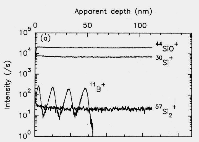
69 Sample Rotation During Ion Bombardment without rotation with rotation SIMS profiles of 11 B ion implantation into 1 µm Al/Si. With sample rotation, B at interface is clearly defined and silicon from Al-Si-Cu layer shows movement to Al/Si interface F. A. Stevie and J. L. Moore, Surf. Interf. Anal. 18, 147 (1992) 69
70 Depth Profiling Analysis Approach Choose primary beam species / secondary polarity Choose primary beam parameters (voltage, raster, current, ) Sample preparation if necessary (remove over-layers) If insulator, prevent sample charging Decide on quantification, determine if standards can be made Depth profile: determine sputtering rates, identify layers Obtain mass spectra: check mass interferences and interfacial contaminants Depth profiles to obtain at least two matching analyses If analyses do not match, check for particles and anomalies 70
Secondary ion mass spectrometry (SIMS)
") Secondary ion mass spectrometry (SIMS) ELEC-L3211 Postgraduate Course in Micro and Nanosciences Department of Micro and Nanosciences Personal motivation and experience on SIMS Offers the possibility to
Secondary ion mass spectrometry (SIMS) ELEC-L3211 Postgraduate Course in Micro and Nanosciences Department of Micro and Nanosciences Personal motivation and experience on SIMS Offers the possibility to
Secondary Ion Mass Spectrometry (SIMS) Thomas Sky
 Thomas Sky") 1 Secondary Ion Mass Spectrometry (SIMS) Thomas Sky Depth (µm) 2 Characterization of solar cells 0,0 1E16 1E17 1E18 1E19 1E20 0,2 0,4 0,6 0,8 1,0 1,2 P Concentration (cm -3 ) Characterization Optimization
1 Secondary Ion Mass Spectrometry (SIMS) Thomas Sky Depth (µm) 2 Characterization of solar cells 0,0 1E16 1E17 1E18 1E19 1E20 0,2 0,4 0,6 0,8 1,0 1,2 P Concentration (cm -3 ) Characterization Optimization
ToF-SIMS or XPS? Xinqi Chen Keck-II
 ToF-SIMS or XPS? Xinqi Chen Keck-II 1 Time of Flight Secondary Ion Mass Spectrometry (ToF-SIMS) Not ToF MS (laser, solution) X-ray Photoelectron Spectroscopy (XPS) 2 3 Modes of SIMS 4 Secondary Ion Sputtering
Characterization of Ultra-Shallow Implants Using Low-Energy Secondary Ion Mass Spectrometry: Surface Roughening under Cesium Bombardment
 Characterization of Ultra-Shallow Implants Using Low-Energy Secondary Ion Mass Spectrometry: Surface Roughening under Cesium Bombardment vyuji Kataoka vmayumi Shigeno vyoko Tada vkazutoshi Yamazaki vmasataka
TECHNIC A L WORK ING GROUP ITWG GUIDELINE ON SECONDARY ION MASS SPECTROMETRY (SIMS)
") NUCLE A R FORENSIC S INTERN ATION A L TECHNIC A L WORK ING GROUP ITWG GUIDELINE ON SECONDARY ION MASS SPECTROMETRY (SIMS) EXECUTIVE SUMMARY Secondary Ion Mass Spectrometry (SIMS) is used for elemental
NUCLE A R FORENSIC S INTERN ATION A L TECHNIC A L WORK ING GROUP ITWG GUIDELINE ON SECONDARY ION MASS SPECTROMETRY (SIMS) EXECUTIVE SUMMARY Secondary Ion Mass Spectrometry (SIMS) is used for elemental
produced a sputter rate of 0.9 nm/s for the radially profiled, un-etched wires. A slightly
 Supporting Information: Beam Current and Sputtering Rate: Using a 16 kev Cs + primary ion beam and a 1 µm 2 rastered area, a 10 pa beam current produced a sputter rate of 0.9 nm/s for the radially profiled,
Secondary-Ion Mass Spectrometry
 Principle of SIMS composition depth profiling with surface analysis techniques? Secondary-Ion Mass Spectrometry erosion of specimen surface by energetic particle bombardment sputtering two possibilities
Secondary ion mass spectrometry (SIMS)
") Secondary ion mass spectrometry (SIMS) Lasse Vines 1 Secondary ion mass spectrometry O Zn 10000 O 2 Counts/sec 1000 100 Li Na K Cr ZnO 10 ZnO 2 1 0 20 40 60 80 100 Mass (AMU) 10 21 10 20 Si 07 Ge 0.3 Atomic
Secondary ion mass spectrometry (SIMS) Lasse Vines 1 Secondary ion mass spectrometry O Zn 10000 O 2 Counts/sec 1000 100 Li Na K Cr ZnO 10 ZnO 2 1 0 20 40 60 80 100 Mass (AMU) 10 21 10 20 Si 07 Ge 0.3 Atomic
Secondary Ion Mass Spectroscopy (SIMS)
") Secondary Ion Mass Spectroscopy (SIMS) Analyzing Inorganic Solids * = under special conditions ** = semiconductors only + = limited number of elements or groups Analyzing Organic Solids * = under special
Secondary Ion Mass Spectroscopy (SIMS) Analyzing Inorganic Solids * = under special conditions ** = semiconductors only + = limited number of elements or groups Analyzing Organic Solids * = under special
cond-mat/ Jul 1998
 Applications of the MRI-model in Sputter Depth Profiling Siegfried Hofmann National Research Institute for Metals 1-2-1 Sengen, Tsukuba, Ibaraki 305 Japan e-mail: siegho@nrim.go.jp The physical principles
Secondary Ion-Mass Spectroscopy (SIMS)
") Secondary Ion-Mass Spectroscopy (SIMS) Prof. Bing-Yue Tsui ( 崔秉鉞 ) Department of Electronics Engineering and Institute of Electronics National Chiao-Tung University 1 Outline Introduction to SIMS Instruments
Secondary Ion-Mass Spectroscopy (SIMS) Prof. Bing-Yue Tsui ( 崔秉鉞 ) Department of Electronics Engineering and Institute of Electronics National Chiao-Tung University 1 Outline Introduction to SIMS Instruments
Introduction to SIMS Basic principles Components Techniques Drawbacks Figures of Merit Variations Resources
 Introduction to SIMS Basic principles Components Techniques Drawbacks Figures of Merit Variations Resources New technique for surface chemical analysis. SIMS examines the mass of ions, instead of energy
PHI 5000 Versaprobe-II Focus X-ray Photo-electron Spectroscopy
 PHI 5000 Versaprobe-II Focus X-ray Photo-electron Spectroscopy The very basic theory of XPS XPS theroy Surface Analysis Ultra High Vacuum (UHV) XPS Theory XPS = X-ray Photo-electron Spectroscopy X-ray
Secondaryionmassspectrometry
 Secondaryionmassspectrometry (SIMS) 1 Incident Ion Techniques for Surface Composition Analysis Mass spectrometric technique 1. Ionization -Electron ionization (EI) -Chemical ionization (CI) -Field ionization
MSE 321 Structural Characterization
 Auger Spectroscopy Auger Electron Spectroscopy (AES) Scanning Auger Microscopy (SAM) Incident Electron Ejected Electron Auger Electron Initial State Intermediate State Final State Physical Electronics
SNMS. SNMS Applications. Combined SIMS and SNMS
 Hiden SIMS SNMS Sputtered Neutral Mass Spectrometry is a quantitative technique using essentially the same instrumentation as SIMS. However, instead of detecting the secondary ions which are formed at
Surface analysis techniques
 Experimental methods in physics Surface analysis techniques 3. Ion probes Elemental and molecular analysis Jean-Marc Bonard Academic year 10-11 3. Elemental and molecular analysis 3.1.!Secondary ion mass
Secondary Ion Mass Spectrometry (SIMS)
") OpenStax-CNX module: m50227 1 Secondary Ion Mass Spectrometry (SIMS) Kourtney Wright Andrew R. Barron This work is produced by OpenStax-CNX and licensed under the Creative Commons Attribution License 4.0
OpenStax-CNX module: m50227 1 Secondary Ion Mass Spectrometry (SIMS) Kourtney Wright Andrew R. Barron This work is produced by OpenStax-CNX and licensed under the Creative Commons Attribution License 4.0
Secondary Ion Mass Spectrometry (SIMS)
") CHEM53200: Lecture 10 Secondary Ion Mass Spectrometry (SIMS) Major reference: Surface Analysis Edited by J. C. Vickerman (1997). 1 Primary particles may be: Secondary particles can be e s, neutral species
CHEM53200: Lecture 10 Secondary Ion Mass Spectrometry (SIMS) Major reference: Surface Analysis Edited by J. C. Vickerman (1997). 1 Primary particles may be: Secondary particles can be e s, neutral species
Ultra Shallow Depth Profiling by Secondary Ion Mass Spectrometry Techniques
 Ultra Shallow Depth Profiling by Secondary Ion Mass Spectrometry Techniques M. Anderle, M. Barozzi, M. Bersani, D. Giubertoni, P. Lazzeri ITCirst, via Sommarive 18, 38050 Povo, Trento, Italy Abstract.
Surface and Interface Characterization of Polymer Films
 Surface and Interface Characterization of Polymer Films Jeff Shallenberger, Evans Analytical Group 104 Windsor Center Dr., East Windsor NJ Copyright 2013 Evans Analytical Group Outline Introduction to
The Controlled Evolution of a Polymer Single Crystal
 Supporting Online Material The Controlled Evolution of a Polymer Single Crystal Xiaogang Liu, 1 Yi Zhang, 1 Dipak K. Goswami, 2 John S. Okasinski, 2 Khalid Salaita, 1 Peng Sun, 1 Michael J. Bedzyk, 2 Chad
MS482 Materials Characterization ( 재료분석 ) Lecture Note 12: Summary. Byungha Shin Dept. of MSE, KAIST
 Lecture Note 12: Summary. Byungha Shin Dept. of MSE, KAIST") 2015 Fall Semester MS482 Materials Characterization ( 재료분석 ) Lecture Note 12: Summary Byungha Shin Dept. of MSE, KAIST 1 Course Information Syllabus 1. Overview of various characterization techniques (1
2015 Fall Semester MS482 Materials Characterization ( 재료분석 ) Lecture Note 12: Summary Byungha Shin Dept. of MSE, KAIST 1 Course Information Syllabus 1. Overview of various characterization techniques (1
Lecture 11 Surface Characterization of Biomaterials in Vacuum
 1 Lecture 11 Surface Characterization of Biomaterials in Vacuum The structure and chemistry of a biomaterial surface greatly dictates the degree of biocompatibility of an implant. Surface characterization
Spontaneous Pattern Formation from Focused and Unfocused Ion Beam Irradiation
 Mat. Res. Soc. Symp. Proc. Vol. 696 2002 Materials Research Society Spontaneous Pattern Formation from Focused and Unfocused Ion Beam Irradiation Alexandre Cuenat and Michael J. Aziz Division of Engineering
Auger Electron Spectroscopy
 Auger Electron Spectroscopy Auger Electron Spectroscopy is an analytical technique that provides compositional information on the top few monolayers of material. Detect all elements above He Detection
Abstract. LOESING, RAINER, Development of High Resolution Depth Profiling Of Ultra Shallow
 Abstract LOESING, RAINER, Development of High Resolution Depth Profiling Of Ultra Shallow Dopant Implants with SIMS (under the direction of Phillip E. Russell) Secondary Ion Mass Spectrometry (SIMS) is
Analysis of Poly(dimethylsiloxane) on Solid Surfaces Using Silver Deposition/TOF-SIMS
 on Solid Surfaces Using Silver Deposition/TOF-SIMS") Special Issue Surface and Micro-Analysis of Organic Materials 21 Research Report Analysis of Poly(dimethylsiloxane) on Solid Surfaces Using Silver Deposition/TOF-SIMS Masae Inoue, Atsushi Murase Abstract
Special Issue Surface and Micro-Analysis of Organic Materials 21 Research Report Analysis of Poly(dimethylsiloxane) on Solid Surfaces Using Silver Deposition/TOF-SIMS Masae Inoue, Atsushi Murase Abstract
ECE Semiconductor Device and Material Characterization
 ECE 4813 Semiconductor Device and Material Characterization Dr. Alan Doolittle School of Electrical and Computer Engineering Georgia Institute of Technology As with all of these lecture slides, I am indebted
Surface and Interface Analysis. Investigations of Molecular Depth Profiling with Dual Beam Sputtering. Journal: Surface and Interface Analysis
 Surface and Interface Analysis Investigations of Molecular Depth Profiling with Dual Beam Sputtering Journal: Surface and Interface Analysis Manuscript ID: Draft Wiley - Manuscript type: SIMS proceedings
( 1+ A) 2 cos2 θ Incident Ion Techniques for Surface Composition Analysis Ion Scattering Spectroscopy (ISS)
 2 cos2 θ Incident Ion Techniques for Surface Composition Analysis Ion Scattering Spectroscopy (ISS)") 5.16 Incident Ion Techniques for Surface Composition Analysis 5.16.1 Ion Scattering Spectroscopy (ISS) At moderate kinetic energies (few hundred ev to few kev) ion scattered from a surface in simple kinematic
5.16 Incident Ion Techniques for Surface Composition Analysis 5.16.1 Ion Scattering Spectroscopy (ISS) At moderate kinetic energies (few hundred ev to few kev) ion scattered from a surface in simple kinematic
Auger Electron Spectroscopy (AES) Prof. Paul K. Chu
 Prof. Paul K. Chu") Auger Electron Spectroscopy (AES) Prof. Paul K. Chu Auger Electron Spectroscopy Introduction Principles Instrumentation Qualitative analysis Quantitative analysis Depth profiling Mapping Examples The Auger
Auger Electron Spectroscopy (AES) Prof. Paul K. Chu Auger Electron Spectroscopy Introduction Principles Instrumentation Qualitative analysis Quantitative analysis Depth profiling Mapping Examples The Auger
Evaluation of Cleaning Methods for Multilayer Diffraction Gratings
 Evaluation of Cleaning Methods for Multilayer Diffraction Gratings Introduction Multilayer dielectric (MLD) diffraction gratings are essential components for the OMEGA EP short-pulse, high-energy laser
Lecture 22 Ion Beam Techniques
 Lecture 22 Ion Beam Techniques Schroder: Chapter 11.3 1/44 Announcements Homework 6/6: Will be online on later today. Due Wednesday June 6th at 10:00am. I will return it at the final exam (14 th June).
X-Ray Photoelectron Spectroscopy (XPS) Prof. Paul K. Chu
 Prof. Paul K. Chu") X-Ray Photoelectron Spectroscopy (XPS) Prof. Paul K. Chu X-ray Photoelectron Spectroscopy Introduction Qualitative analysis Quantitative analysis Charging compensation Small area analysis and XPS imaging
X-Ray Photoelectron Spectroscopy (XPS) Prof. Paul K. Chu X-ray Photoelectron Spectroscopy Introduction Qualitative analysis Quantitative analysis Charging compensation Small area analysis and XPS imaging
MSE 321 Structural Characterization
 Auger Spectroscopy Auger Electron Spectroscopy (AES) Scanning Auger Microscopy (SAM) Incident Electron Ejected Electron Auger Electron Initial State Intermediate State Final State Physical Electronics
Secondary Ion Mass Spectrometry (SIMS) for Surface Analysis
 for Surface Analysis") Secondary Ion Mass Spectrometry (SIMS) for Surface Analysis General overview of SIMS - principles, ionization, advantages & limitations SIMS as a surface analysis technique - operation modes, information
Secondary Ion Mass Spectrometry (SIMS) for Surface Analysis General overview of SIMS - principles, ionization, advantages & limitations SIMS as a surface analysis technique - operation modes, information
ION BEAM TECHNIQUES. Ion beam characterization techniques are illustrated in Fig
 ION BEAM TECHNIQUES Ion beam characterization techniques are illustrated in Fig. 11.21. 1 ION BEAM TECHNIQUES Incident ions are absorbed, emitted, scattered, or reflected leading to light, electron or
MS482 Materials Characterization ( 재료분석 ) Lecture Note 4: XRF
 Lecture Note 4: XRF") 2016 Fall Semester MS482 Materials Characterization ( 재료분석 ) Lecture Note 4: XRF Byungha Shin Dept. of MSE, KAIST 1 Course Information Syllabus 1. Overview of various characterization techniques (1 lecture)
2016 Fall Semester MS482 Materials Characterization ( 재료분석 ) Lecture Note 4: XRF Byungha Shin Dept. of MSE, KAIST 1 Course Information Syllabus 1. Overview of various characterization techniques (1 lecture)
Secondary Ion Mass Spectrometry
 Secondary Ion Mass Spectrometry Timothy P. Spila, Ph.D. Frederick Seitz Materials Research Laboratory University of Illinois at Urbana-Champaign Secondary Ion Mass Spectrometry SIMS is an analytical technique
Supplementary Figure 1: AFM topography of the graphene/sio 2 [(a) and (c)] and graphene/h BN [(b) and (d)] surfaces acquired before [(a) and (b)],
![Supplementary Figure 1: AFM topography of the graphene/sio 2 [(a) and (c)] and graphene/h BN [(b) and (d)] surfaces acquired before [(a) and (b)],](/thumbs/94/121705311.jpg "Supplementary Figure 1: AFM topography of the graphene/sio 2 [(a) and (c)] and graphene/h BN [(b) and (d)] surfaces acquired before [(a) and (b)],") Supplementary Figure 1: AFM topography of the graphene/sio 2 [(a) and (c)] and graphene/h BN [(b) and (d)] surfaces acquired before [(a) and (b)], and after [(c) and (d)], respectively, 35 seconds of Cs
Supplementary Figure 1: AFM topography of the graphene/sio 2 [(a) and (c)] and graphene/h BN [(b) and (d)] surfaces acquired before [(a) and (b)], and after [(c) and (d)], respectively, 35 seconds of Cs
CIM PACA Characterisation Lab
 CIM PACA Characterisation Lab Your partner of choice for the chemical characterisation of your materials Partners: Who are we? The CIM PACA Characterisation Lab was registered in 2005 as a not-for-profit
High-Precision Evaluation of Ultra-Shallow Impurity Profiles by Secondary Ion Mass Spectrometry
 High-Precision Evaluation of Ultra-Shallow Impurity Profiles by Secondary Ion Mass Spectrometry Yoko Tada Kunihiro Suzuki Yuji Kataoka (Manuscript received December 28, 2009) As complementary metal oxide
Secondary Ion Mass Spectrometry (SIMS) for Surface Analysis
 for Surface Analysis") Secondary Ion Mass Spectrometry (SIMS) for Surface Analysis General overview of SIMS - principles, ionization, advantages & limitations SIMS as a surface analysis technique - operation modes, information
Secondary Ion Mass Spectrometry (SIMS) for Surface Analysis General overview of SIMS - principles, ionization, advantages & limitations SIMS as a surface analysis technique - operation modes, information
IONTOF. Latest Developments in 2D and 3D TOF-SIMS Analysis. Surface Analysis Innovations and Solutions for Industry 2017 Coventry
 Latest Developments in 2D and 3D TOF-SIMS Analysis Surface Analysis Innovations and Solutions for Industry 2017 Coventry 12.10.2017 Matthias Kleine-Boymann Regional Sales Manager matthias.kleine-boymann@iontof.com
Nanoscale Chemical Characterization: Moving to 3 Dimensions
 Nanoscale Chemical Characterization: Moving to 3 Dimensions Eric B. Steel Chemical Science & Technology Laboratory National Institute of Standards & Technology Outline What is and why do we need chemical
Applications of XPS, AES, and TOF-SIMS
 Applications of XPS, AES, and TOF-SIMS Scott R. Bryan Physical Electronics 1 Materials Characterization Techniques Microscopy Optical Microscope SEM TEM STM SPM AFM Spectroscopy Energy Dispersive X-ray
The second part of this study examined depth profiles of sample surfaces that have been previously exposed to Cs primary beam.
 ABSTRACT PENLEY, CHRISTOPHER RANDY. Cesium Neutral Beam and Surface Oxidation Effects on SIMS Analysis at Surface of Silicon. (Under the direction of Dr. Dieter P. Griffis.) The effects of sample aging
Gaetano L Episcopo. Scanning Electron Microscopy Focus Ion Beam and. Pulsed Plasma Deposition
 Gaetano L Episcopo Scanning Electron Microscopy Focus Ion Beam and Pulsed Plasma Deposition Hystorical background Scientific discoveries 1897: J. Thomson discovers the electron. 1924: L. de Broglie propose
The Benefit of Wide Energy Range Spectrum Acquisition During Sputter Depth Profile Measurements
 The Benefit of Wide Energy Range Spectrum Acquisition During Sputter Depth Profile Measurements Uwe Scheithauer, 82008 Unterhaching, Germany E-Mail: scht.uhg@googlemail.com Internet: orcid.org/0000-0002-4776-0678;
MS482 Materials Characterization ( 재료분석 ) Lecture Note 5: RBS
 Lecture Note 5: RBS") 2016 Fall Semester MS482 Materials Characterization ( 재료분석 ) Lecture Note 5: RBS Byungha Shin Dept. of MSE, KAIST 1 Course Information Syllabus 1. Overview of various characterization techniques (1 lecture)
2016 Fall Semester MS482 Materials Characterization ( 재료분석 ) Lecture Note 5: RBS Byungha Shin Dept. of MSE, KAIST 1 Course Information Syllabus 1. Overview of various characterization techniques (1 lecture)
Ion Implantation. alternative to diffusion for the introduction of dopants essentially a physical process, rather than chemical advantages:
 Ion Implantation alternative to diffusion for the introduction of dopants essentially a physical process, rather than chemical advantages: mass separation allows wide varies of dopants dose control: diffusion
SURFACE PROCESSING WITH HIGH-ENERGY GAS CLUSTER ION BEAMS
 SURFACE PROCESSING WITH HIGH-ENERGY GAS CLUSTER ION BEAMS Toshio Seki and Jiro Matsuo, Quantum Science and Engineering Center, Kyoto University, Gokasyo, Uji, Kyoto 611-0011, Japan Abstract Gas cluster
Single ion implantation for nanoelectronics and the application to biological systems. Iwao Ohdomari Waseda University Tokyo, Japan
 Single ion implantation for nanoelectronics and the application to biological systems Iwao Ohdomari Waseda University Tokyo, Japan Contents 1.History of single ion implantation (SII) 2.Novel applications
Hiden SIMS Secondary Ion Mass Spectrometers. Analysers for surface, elemental and molecular analysis
 Hiden SIMS Secondary Ion Mass Spectrometers Analysers for surface, elemental and molecular analysis vacuum analysis surface science plasma diagnostics gas analysis SIMS Versatility SIMS is a high sensitivity
Polymer/drug films as a model system for a drug eluting coronary stent coating layer
 Polymer/drug films as a model system for a drug eluting coronary stent coating layer Valeria Ciarnelli Prof. Clive Roberts Prof. Morgan Alexander, Prof. Martyn Davies School of Pharmacy The University
Auger Electron Spectroscopy Overview
 Auger Electron Spectroscopy Overview Also known as: AES, Auger, SAM 1 Auger Electron Spectroscopy E KLL = E K - E L - E L AES Spectra of Cu EdN(E)/dE Auger Electron E N(E) x 5 E KLL Cu MNN Cu LMM E f E
G. Pepponi, a D. Giubertoni, and M. Bersani CMM-Irst, Fondazione Bruno Kessler, via Sommarive 18, Povo, Trento, Italy
 Grazing incidence x-ray fluorescence and secondary ion mass spectrometry combined approach for the characterization of ultrashallow arsenic distribution in silicon G. Pepponi, a D. Giubertoni, and M. Bersani
Imaging Methods: Scanning Force Microscopy (SFM / AFM)
") Imaging Methods: Scanning Force Microscopy (SFM / AFM) The atomic force microscope (AFM) probes the surface of a sample with a sharp tip, a couple of microns long and often less than 100 Å in diameter.
Imaging Methods: Scanning Force Microscopy (SFM / AFM) The atomic force microscope (AFM) probes the surface of a sample with a sharp tip, a couple of microns long and often less than 100 Å in diameter.
Surface Analysis. Dr. Lynn Fuller Dr. Fuller s Webpage:
 ROCHESTER INSTITUTE OF TECHNOLOGY MICROELECTRONIC ENGINEERING Surface Analysis Dr. Lynn Fuller Dr. Fuller s Webpage: http://people.rit.edu/lffeee 82 Lomb Memorial Drive Rochester, NY 14623-5604 Tel (585)
Direct-Write Deposition Utilizing a Focused Electron Beam
 Direct-Write Deposition Utilizing a Focused Electron Beam M. Fischer, J. Gottsbachner, S. Müller, W. Brezna, and H.D. Wanzenboeck Institute of Solid State Electronics, Vienna University of Technology,
Investigation of the bonding strength and interface current of p-siõn-gaas wafers bonded by surface activated bonding at room temperature
 Investigation of the bonding strength and interface current of p-siõn-gaas wafers bonded by surface activated bonding at room temperature M. M. R. Howlader, a) T. Watanabe, and T. Suga Research Center
Supplementary Figure 1 Detailed illustration on the fabrication process of templatestripped
 Supplementary Figure 1 Detailed illustration on the fabrication process of templatestripped gold substrate. (a) Spin coating of hydrogen silsesquioxane (HSQ) resist onto the silicon substrate with a thickness
Ion Implant Part 1. Saroj Kumar Patra, TFE4180 Semiconductor Manufacturing Technology. Norwegian University of Science and Technology ( NTNU )
") 1 Ion Implant Part 1 Chapter 17: Semiconductor Manufacturing Technology by M. Quirk & J. Serda Spring Semester 2014 Saroj Kumar Patra,, Norwegian University of Science and Technology ( NTNU ) 2 Objectives
1 Ion Implant Part 1 Chapter 17: Semiconductor Manufacturing Technology by M. Quirk & J. Serda Spring Semester 2014 Saroj Kumar Patra,, Norwegian University of Science and Technology ( NTNU ) 2 Objectives
Effect of Spiral Microwave Antenna Configuration on the Production of Nano-crystalline Film by Chemical Sputtering in ECR Plasma
 THE HARRIS SCIENCE REVIEW OF DOSHISHA UNIVERSITY, VOL. 56, No. 1 April 2015 Effect of Spiral Microwave Antenna Configuration on the Production of Nano-crystalline Film by Chemical Sputtering in ECR Plasma
Observations Regarding Automated SEM and SIMS Analysis of Minerals. Kristofor Ingeneri. April 22, 2009
 Observations Regarding Automated SEM and SIMS Analysis of Minerals Kristofor Ingeneri April 22, 2009 Forensic Geoscience A field of inquiry that utilizes techniques developed in the geosciences (geology,
Accepted Manuscript. Authors: Charbel S. Madi, Michael J. Aziz S (11) Reference: APSUSC 22249
 Reference: APSUSC 22249") Title: Multiple Scattering Causes the Low Energy Low Angle Constant Wavelength Topographical Instability of Argon Ion Bombarded Silicon surfaces Authors: Charbel S. Madi, Michael J. Aziz PII: S0169-4332(11)01226-8
Title: Multiple Scattering Causes the Low Energy Low Angle Constant Wavelength Topographical Instability of Argon Ion Bombarded Silicon surfaces Authors: Charbel S. Madi, Michael J. Aziz PII: S0169-4332(11)01226-8
NUCLEAR TRANSMUTATION IN DEUTERED PD FILMS IRRADIATED BY AN UV LASER
 Castellano, et al. Nuclear Transmutation in Deutered Pd Films Irradiated by an UV Laser. in 8th International Conference on Cold Fusion. 2000. Lerici (La Spezia), Italy: Italian Physical Society, Bologna,
Nanocrystalline Si formation inside SiN x nanostructures usingionized N 2 gas bombardment
 연구논문 한국진공학회지제 16 권 6 호, 2007 년 11 월, pp.474~478 Nanocrystalline Si formation inside SiN x nanostructures usingionized N 2 gas bombardment Min-Cherl Jung 1, Young Ju Park 2, Hyun-Joon Shin 1, Jun Seok Byun
Reduced preferential sputtering of TiO 2 (and Ta 2 O 5 ) thin films through argon cluster ion bombardment.
 thin films through argon cluster ion bombardment.") NATIOMEM Reduced preferential sputtering of TiO 2 (and Ta 2 O 5 ) thin films through argon cluster ion bombardment. R. Grilli *, P. Mack, M.A. Baker * * University of Surrey, UK ThermoFisher Scientific
NATIOMEM Reduced preferential sputtering of TiO 2 (and Ta 2 O 5 ) thin films through argon cluster ion bombardment. R. Grilli *, P. Mack, M.A. Baker * * University of Surrey, UK ThermoFisher Scientific
Early History of the AVS Topical Conferences On Quantitative Surface Analysis
 Early History of the AVS Topical Conferences On Quantitative Surface Analysis 1. The Start (1986) 2. 1987 through 2003 Cedric Powell National Institute of Standards and Technology, Gaithersburg 3. Later
Surface Defects on Natural MoS 2
 Supporting Information: Surface Defects on Natural MoS 2 Rafik Addou 1*, Luigi Colombo 2, and Robert M. Wallace 1* 1 Department of Materials Science and Engineering, The University of Texas at Dallas,
Diffusion and Ion implantation Reference: Chapter 4 Jaeger or Chapter 3 Ruska N & P Dopants determine the resistivity of material Note N lower
 Diffusion and Ion implantation Reference: Chapter 4 Jaeger or Chapter 3 Ruska N & P Dopants determine the resistivity of material Note N lower resistavity than p: due to higher carrier mobility Near linear
FIB - SIMS. Focussed Ion Beam Secondary Ion Mass Spectrometry.
 FIB - SIMS Focussed Ion Beam Secondary Ion Mass Spectrometry Outline Introduction to Hiden Analytical Introduction to SIMS FIB-SIMS - Introduction and key features FIB-SIMS - Applications data Hiden SIMS
Infrastructure of Thin Films Laboratory in Institute of Molecular Physics Polish Academy of Sciences
 Infrastructure of Thin Films Laboratory in Institute of Molecular Physics Polish Academy of Sciences Outline Sample preparation Magnetron sputtering Ion-beam sputtering Pulsed laser deposition Electron-beam
Molecular Weight Evaluation of Poly(dimethylsiloxane) on Solid Surfaces Using Silver Deposition/TOF-SIMS
 on Solid Surfaces Using Silver Deposition/TOF-SIMS") ANALYTICAL SCIENCES DECEMBER 2004, VOL. 20 2004 The Japan Society for Analytical Chemistry 1623 The Best Paper in Bunseki Kagaku, 2003 Molecular Weight Evaluation of Poly(dimethylsiloxane) on Solid Surfaces
ANALYTICAL SCIENCES DECEMBER 2004, VOL. 20 2004 The Japan Society for Analytical Chemistry 1623 The Best Paper in Bunseki Kagaku, 2003 Molecular Weight Evaluation of Poly(dimethylsiloxane) on Solid Surfaces
Review. Surfaces of Biomaterials. Characterization. Surface sensitivity
 Surfaces of Biomaterials Three lectures: 1.23.05 Surface Properties of Biomaterials 1.25.05 Surface Characterization 1.27.05 Surface and Protein Interactions Review Bulk Materials are described by: Chemical
AP5301/ Name the major parts of an optical microscope and state their functions.
 Review Problems on Optical Microscopy AP5301/8301-2015 1. Name the major parts of an optical microscope and state their functions. 2. Compare the focal lengths of two glass converging lenses, one with
Check the LCLS Project website to verify 2 of 6 that this is the correct version prior to use.
 1. Introduction The XTOD Offset Systems are designed to spatially separate the useful FEL radiation from high-energy spontaneous radiation and Bremsstrahlung γ-rays. These unwanted radiations are generated
Segregated chemistry and structure on (001) and (100) surfaces of
 and (100) surfaces of") Supporting Information Segregated chemistry and structure on (001) and (100) surfaces of (La 1-x Sr x ) 2 CoO 4 override the crystal anisotropy in oxygen exchange kinetics Yan Chen a, Helena Téllez b,c,
Supporting Information Segregated chemistry and structure on (001) and (100) surfaces of (La 1-x Sr x ) 2 CoO 4 override the crystal anisotropy in oxygen exchange kinetics Yan Chen a, Helena Téllez b,c,
Application of the GD-Profiler 2 to the PV domain
 Application of the GD-Profiler 2 to the PV domain GD Profiler 2 RF GDOES permits to follow the distribution of the elements as function of depth. This is an ultra fast characterisation technique capable
Secondary Ion Mass Spectrometry (SIMS)
") Secondary Ion Mass Spectrometry (SIMS) SIMS: a desorption/ionization technique 1960s - A. Benninghoven, University of Münster, Germany (Benninghoven A., Rudenauer F.G., Werner H.W., Secondary Ion Mass
Secondary Ion Mass Spectrometry (SIMS) SIMS: a desorption/ionization technique 1960s - A. Benninghoven, University of Münster, Germany (Benninghoven A., Rudenauer F.G., Werner H.W., Secondary Ion Mass
Removal of Cu Impurities on a Si Substrate by Using (H 2 O 2 +HF) and (UV/O 3 +HF)
 and (UV/O 3 +HF)") Journal of the Korean Physical Society, Vol. 33, No. 5, November 1998, pp. 579 583 Removal of Cu Impurities on a Si Substrate by Using (H 2 O 2 +HF) and (UV/O 3 +HF) Baikil Choi and Hyeongtag Jeon School
Journal of the Korean Physical Society, Vol. 33, No. 5, November 1998, pp. 579 583 Removal of Cu Impurities on a Si Substrate by Using (H 2 O 2 +HF) and (UV/O 3 +HF) Baikil Choi and Hyeongtag Jeon School
MSN551 LITHOGRAPHY II
 MSN551 Introduction to Micro and Nano Fabrication LITHOGRAPHY II E-Beam, Focused Ion Beam and Soft Lithography Why need electron beam lithography? Smaller features are required By electronics industry:
Photon Energy Dependence of Contrast in Photoelectron Emission Microscopy of Si Devices
 Photon Energy Dependence of Contrast in Photoelectron Emission Microscopy of Si Devices V. W. Ballarotto, K. Siegrist, R. J. Phaneuf, and E. D. Williams University of Maryland and Laboratory for Physical
Keywords: Abstract. Uwe Scheithauer. Unterhaching
 Sputter Induced Cross Contaminations in Analytical AES and XPS Instrumentation: Utilization of the effect for the In situ Deposition of Ultrathin Functional Layers Uwe Scheithauer Unterhaching Phone: +49
Chapter 8 Ion Implantation
 Chapter 8 Ion Implantation 2006/5/23 1 Wafer Process Flow Materials IC Fab Metalization CMP Dielectric deposition Test Wafers Masks Thermal Processes Implant PR strip Etch PR strip Packaging Photolithography
EDS Mapping. Ian Harvey Fall Practical Electron Microscopy
 EDS Mapping Ian Harvey Fall 2008 1 From: Energy Dispersive X-ray Microanalysis, An Introduction Kevex Corp. 1988 Characteristic X-ray generation p.2 1 http://www.small-world.net/efs.htm X-ray generation
A. Burenkov, P. Pichler, J. Lorenz, Y. Spiegel, J. Duchaine, F. Torregrosa
 Simulation of Plasma Immersion Ion Implantation A. Burenkov, P. Pichler, J. Lorenz, Y. Spiegel, J. Duchaine, F. Torregrosa 2011 International Conference on Simulation of Semiconductor Processes and Devices
Surface Chemistry and Reaction Dynamics of Electron Beam Induced Deposition Processes
 Surface Chemistry and Reaction Dynamics of Electron Beam Induced Deposition Processes e -? 2 nd FEBIP Workshop Thun, Switzerland 2008 Howard Fairbrother Johns Hopkins University Baltimore, MD, USA Outline
XPS & Scanning Auger Principles & Examples
 XPS & Scanning Auger Principles & Examples Shared Research Facilities Lunch Talk Contact info: dhu Pujari & Han Zuilhof Lab of rganic Chemistry Wageningen University E-mail: dharam.pujari@wur.nl Han.Zuilhof@wur.nl
Electrical Characterization with SPM Application Modules
 Electrical Characterization with SPM Application Modules Metrology, Characterization, Failure Analysis: Data Storage Magnetoresistive (MR) read-write heads Semiconductor Transistors Interconnect Ferroelectric
Microscopy AND Microanalysis MICROSCOPY SOCIETY OF AMERICA 2006
 Microsc. Microanal. 12, 340 346, 2006 DOI: 10.1017/S1431927606060442 Microscopy AND Microanalysis MICROSCOPY SOCIETY OF AMERICA 2006 The Low Energy X-ray Spectrometry Technique as Applied to Semiconductors
Soft X-ray multilayer mirrors by ion assisted sputter deposition
 Soft X-ray multilayer mirrors by ion assisted sputter deposition Valentino Rigato INFN Laboratori Nazionali di Legnaro Bologna, September 21, 2010 Source: INFN-LNL-2009 V. RIGATO 1 SIF- Bologna September
Changing the Dopant Concentration. Diffusion Doping Ion Implantation
 Changing the Dopant Concentration Diffusion Doping Ion Implantation Step 11 The photoresist is removed with solvent leaving a ridge of polysilicon (the transistor's gate), which rises above the silicon
MS482 Materials Characterization ( 재료분석 ) Lecture Note 5: RBS. Byungha Shin Dept. of MSE, KAIST
 Lecture Note 5: RBS. Byungha Shin Dept. of MSE, KAIST") 2015 Fall Semester MS482 Materials Characterization ( 재료분석 ) Lecture Note 5: RBS Byungha Shin Dept. of MSE, KAIST 1 Course Information Syllabus 1. Overview of various characterization techniques (1 lecture)
2015 Fall Semester MS482 Materials Characterization ( 재료분석 ) Lecture Note 5: RBS Byungha Shin Dept. of MSE, KAIST 1 Course Information Syllabus 1. Overview of various characterization techniques (1 lecture)
Electron beam scanning
 Electron beam scanning The Electron beam scanning operates through an electro-optical system which has the task of deflecting the beam Synchronously with cathode ray tube which create the image, beam moves
Surface and Thin Film Analysis with Electron and Mass Spectrometric Techniques
 Surface and Thin Film Analysis with Electron and Mass Spectrometric Techniques A. Wucher Fachbereich Physik, Universität Kaiserslautern D-67653 Kaiserslautern Abstract We give a short overview of recent
Depth Distribution Functions of Secondary Electron Production and Emission
 Depth Distribution Functions of Secondary Electron Production and Emission Z.J. Ding*, Y.G. Li, R.G. Zeng, S.F. Mao, P. Zhang and Z.M. Zhang Hefei National Laboratory for Physical Sciences at Microscale
Surface Science Spectra
 Surface Science Spectra WCF Submission 226 Proof - SSS Submission # 14-015 (20141102)V22 Analysis of Silicon Germanium Standards for the Quantification of SiGe Microelectronic Devices using AES SECTION