Chemical Exfoliation of graphene and other 2D-materials
|
|
|
- Peregrine Young
- 6 years ago
- Views:
Transcription
1 Chemical Exfoliation of graphene and other 2D-materials A thesis submitted to The University of Manchester for the degree of Master of Philosophy in the Faculty of Engineering and Physical Sciences Sukhraaj Johal School of Chemistry 1
2 Abstract Graphene has been described as a miracle material and since its isolation in 2004 there have been thousands of reports of its exceptional properties and the wide range of applications it could be incorporated into. This thesis focuses on several topics; the first being the liquid exfoliation of graphite using surfactant like 1 pyrenesulfonic acid sodium salt (1-PSA), this dispersion was produced using the sonication method and it was found the single-layer yield was ~ 20%. A graphene paper was produced using this dispersion and a second was produced from sonication of graphite in N-Methyl-2-pyrrolidone (NMP). The second paper was produced as a reference as it has been well characterised in previous studies. X-ray Photoelectron Spectroscopy (XPS) was performed on both papers to check no graphene oxide or graphene derivative had been produced. It was found there was a ~ 14% residual of 1-PSA molecules present in the 1-PSA based paper, compared to ~ 8% residual NMP in the corresponding paper. The second topic covers the transfer of anodic bonding graphene samples in solution. This technique allows deposition of mostly single and few-layer graphene flakes onto a glass substrate. The transfer method we adopted was to use cellulose acetate butyrate (CAB) in ethyl acetate, which forms a film, encapsulating the flakes on the substrate. These films can then be dissolved in ethyl acetate. Although, we had promising results at the beginning of this study, it was concluded that the graphene flakes were embedded in the CAB films and the cellulose could not be removed. The third part shows preliminary results on the production of new 2D materials using the solvent based and 1-PSA based exfoliation methods. These show promising results as longer sonication times are proving successful in producing thinner flakes. 2
3 List of figures Figure 1-2D graphene sheets can be wrapped up into 0D fullerenes, rolled into 1D nanotubes and stacked into 3D graphite. [8]... 8 Figure 2 - a) Crystal lattice and b) Brillouin zone of graphene. c) Dirac points are located at points K and K'. Energy band close to Dirac point. The inset shows the Dirac cones at low energy. Adapted from [11] Figure 3 - Parabolic conduction band approximation Figure 4 - Ambipolar electric field effect in monolayer graphene. The insets show the changes in the position of the Fermi energy, E F, with changing gate voltage, V g. [15] Figure 5 - Left: Optical picture of large flake consisting of 1, 2, 3 and 6 layers of graphene. Right: the corresponding Raman spectra of the layers Figure 6 - Schematic of the experimental setup used to measure the breaking strength of graphene [22] Figure 7 - Anodic bonding experimental setup Figure 8-1-PSA Figure 9 - General coordination geometry of MoX2 compounds Figure 10 - a) Schematic of the exfoliation method using 1-PSA. b) Graphene dispersion obtained. c) Graphene paper produced Figure 11 - a) optical picture of as deposited graphene on a glass substrate. b) optical picture of same graphene sheet transferred onto new glass slide. c) optical picture of second as deposited graphene on a glass substrate. d) optical picture taken after transferred onto Si/ SiO 2 substrate Figure 12 - Phonon band structure of graphene derived from DFT calculations. The LO, LA and ito phonon are displayed. The Kohn anomalies at Г and K are emphasised by red lines. Adapted from [61] Figure 13 - Raman spectrum of monolayer graphene Figure 14 - Raman activation mechanism of the 2D peak Figure 15 - Evolution of the 2D peak from graphite to graphene Figure 16 - Picture of Raman system Figure 17 - XPS results for 1-PSA based graphene paper. Left: C1S spectrum and right: survey spectrum Figure 18 - XPS results of NMP-based graphene paper. Left: survey spectrum and right: C1S spectrum Figure 19 - Comparison of Raman spectra of 1-PSA-/ NMP- based graphene papers Figure 20 - Optical pictures of EtOH dispersion on Si/SiO 2 substrate Figure 21 - Optical pictures of IPA dispersion on Si/SiO 2 substrate. Black circle: residual IPA. Red circle: graphene flakes Figure 22 - Raman spectrum of flakes found in IPA dispersion Figure 23 - Optical pictures of Si/SiO 2 substrate once 10 µl (left) and 8 µl (right) of CAB solution was dropped Figure 24 - Left: Optical picture of Si/SiO 2 substrate with flakes visible. Right: Raman spectrum of flake. Red X marks where flakes were found Figure 25 - a) optical picture and b) Raman spectrum of flakes after 9 hours sonication and 3 hours washing time in ethyl acetate. c) and d) optical pictures of substrate after 9 hours 3
4 sonication and washing overnight in ethyl acetate.. Red X marks where flakes were found Figure 26 - a) optical picture and b) Raman spectrum of sample sonicated for 24 hours. c) optical picture and d) Raman spectrum of sample sonicated for 72 hours.. Red X marks where flakes were found Figure 27 - Optical pictures and typical Raman spectrum of flakes encapsulated in CAB film. Red X marks where flakes were found Figure 28 - AFM image of MoTe 2 sonicated for 3 hours (left) and 24 hours (right) Figure 29 - AFM images of MoSe 2 in IPA sonicated for 3 hours (left) and 24 hours (right) Figure 30 - Left: MoTe 2 in 4 mg/ ml of 1-PSA solution. Right: MoSe 2 in 3 mg/ ml of 1-PSA solution Figure 31 - Left: Raman spectrum of MoSe 2. Right: Raman spectrum of MoTe
5 Contents Abstract... 2 List of figures Introduction Carbon Graphene electronic structure Graphene properties Electronic properties Optical properties Mechanical properties Graphene applications i) Field Effect Transistor (FET) ii) Transparent conductive electrodes iii) Gas detectors and sensors iv) Batteries Graphene: Production routes i) Micromechanical cleavage ii) Anodic bonding iii) Chemical vapour deposition (CVD) iv) Chemical exfoliation of graphite D layered materials Aims and objectives Experimental and Characterisation Graphene papers preparation Transfer of Anodic bonded samples in suspension Transition metal dichalogenides Solvent sonication method PSA method Characterisation Raman spectroscopy Atomic force microscopy (AFM) X-ray Photoelectron Spectroscopy (XPS) Results and discussion Graphene papers
6 3.1.2 XPS results Raman spectroscopy results Anodic bonding samples Transfer based on solvent and sonication Transfer with Cellulose acetate butyrate (CAB) Transition metal dichalogenides (TMDs) Conclusions and future work Appendices References
7 1. Introduction 1.1 Carbon Forming a diverse range of materials, carbon can be classed as an extraordinary element. This is a result of the s and p-orbitals of carbon being able to hybridise into sp-, sp 2 - and sp 3 - bonds. For example, diamond is a 3-dimensional (3D) solid made up of sp 3 bonded carbons in a tetrahedral shape; whereas graphite is made up of 2-dimensional (2D) sheets containing sp 2 bonded carbons. Bonding can affect the properties of these materials; diamond is an insulator whereas graphite can conduct electricity. Hybridisation is not the only parameter that can determine the properties of a material, dimensionality is also important. [1] Carbon can form a number of inorganic allotropes with different dimensionality; graphite (3D), fullerenes (0D), nanotubes (1D) and the most recently discovered: graphene (2D). [2-9] Graphene is a single layer of sp 2 hybridised carbon atoms packed into a hexagonal lattice. A trigonal planar structure is observed due to the s, p(x) and p(y) orbitals forming σ- bonds, 142 pm in length. The p(z) orbitals of neighbouring carbon atoms interact forming a π-band, which makes up the delocalised network of electrons. Graphene is the basic building block of all other graphitic material [8] (Figure 1). The sheets can be stacked into layers forming 3D graphite, with an interlayer spacing of 0.335nm, held together by weak Van der Waals forces. Spherically arranged carbon atoms make up fullerene; where some of the hexagonal lattices are replaced by pentagons, which give them their curvature. This spherical arrangement produces discrete energy levels so that fullerenes can be seen as 0D materials. [2] Rolling up sheets produces 1D nanotubes; they have outstanding properties which strongly depend on the direction the graphene sheet is rolled to form the tube, this can make them either metallic or semiconducting in nature and will also possess different optical transition energies which make them interesting for various applications. [1] 7

8 Dimensionality strongly affects the properties of a material. Graphene and graphite have the same planar structure and hybridisation. However, they have very different optical, electronic and mechanical properties. Figure 1-2D graphene sheets can be wrapped up into 0D fullerenes, rolled into 1D nanotubes and stacked into 3D graphite. [8] 1.2 Graphene electronic structure The band structure of graphene was originally stated by P. R. Wallace in 1948, to be semi-metallic[10]. We now know graphene is a semimetal/ zero bandgap semiconductor (Figure 2). The crystal lattice of graphene contains two sublattices containing atoms A and B, which make up the unit cell (Figure 2a). 8

9 Figure 2 - a) Crystal lattice and b) Brillouin zone of graphene. c) Dirac points are located at points K and K'. Energy band close to Dirac point. The inset shows the Dirac cones at low energy. Adapted from [11]. Going from real space to reciprocal space, the Brillouin zone is also hexagonal, the centre is the Γ point and the non-equivalent corners are the K and K points, where there is high symmetry, also called Dirac points. The K and K points are inequivalent as they relate to the atoms A and B in the unit cell. By overlapping two graphene sublattices, two energy bands are formed; the valence band (bottom cone) and conduction band (top cone) which only meet at the six Dirac points at the corners of the Brillouin zone. This crystal structure produces a linear electronic band structure at the K and K Dirac points at low energy. The Fermi energy, E F, lies at the Dirac point. At low energy, the energy of the electronic states varies linearly with momentum of the charge carriers. Thus, quasiparticles in graphene exhibit a linear dispersion relation: E= ±ћv F Where v F is Fermi velocity ~10 6 m/s, Kx and Ky are components of the momentum in the direction x and y (Figure 2c inset). [12] Conventional semiconductors show a parabolic conduction and valence band, which are separated by a small gap (1-2 ev). e.g. silicon [8] (Figure 3). 9

10 Figure 3 - Parabolic conduction band approximation In this case, the electrons are described using the Schrödinger equation. However in graphene the linear dispersion between energy and momentum means the electrons within graphene maintain a constant speed and are described using the Dirac equation, as they behave as massless relativistic particles. [8, 13, 14] 1.3 Graphene properties Electronic properties Graphene s linear energy dispersion at low energies (near the 6 corners of the Brillouin zone) gives electrons their zero-effective mass, meaning they travel at a constant speed, equal to 10 6 m/s. Thus, the graphene charge mobility is essentially independent of temperature, T, and is limited only by defect scattering. [14] If graphene is placed in a device configuration, i.e. it is contacted with a source, drain and gate voltage, V g, then graphene will show an ambipolar electric field; the charge carriers can be tuned between electrons and holes [15] (Figure 4). 10
 due to the independence of mobility between 10 and 100K.")
11 Figure 4 - Ambipolar electric field effect in monolayer graphene. The insets show the changes in the position of the Fermi energy, E F, with changing gate voltage, V g. [15] There is a potential of obtaining high mobilities at room temperature (R.T.) due to the independence of mobility between 10 and 100K. [15] Mobility remains high even at high carrier densities, resulting in the electrons travelling through a sheet with negligible electrical resistivity, i.e. the electrons can travel micrometres in length before hitting other atoms or defects in the structure and being scattered. [16] This is called ballistic transport. Graphene also shows exotic properties when it is immersed in magnetic fields. [17] Optical properties For a single atomic layer, graphene has an unexpectedly high absorbance (~ 2.3%) of visible light. [14] The fraction of visible light it absorbs is attributed to its unique electronic structure that features electron and hole canonical bands which meet at the Dirac point. [18] The Dirac Fermions high frequency conductivity is constant from the Infra-red (IR) region through to the visible range. The rest of the light is transmitted through graphene, i.e. graphene is essentially transparent when deposited on a substrate, and thus it is particularly challenging to locate graphene flakes among thicker flakes. The type of substrate used to deposit graphene can 11
. i.e. even a single layer of graphene on an oxidised silicon substrate can give enough contrast for it to be spotted under an optical microscope.")
12 make a difference to its optical visibility. Oxidised silicon is a popular choice and it has been shown that an oxide layer of 90/ 300 nm, on top of silicon, shows maximum optical enhancement of graphene (~ 12%). i.e. even a single layer of graphene on an oxidised silicon substrate can give enough contrast for it to be spotted under an optical microscope. [19, 20] The oxide layer causes light interference with the incident and reflected light, enhancing the visibility of graphene on the substrate. [21, 19] Figure 5 shows an optical picture of a graphene flake composed of multiple layers and the corresponding Raman spectrum of the different layers. A darker colour is consistent with thicker layers; however, once above 10 layers this trend does not continue. [21] Figure 5 - Left: Optical picture of large flake consisting of 1, 2, 3 and 6 layers of graphene. Right: the corresponding Raman spectra of the layers Mechanical properties Graphene has recently been shown to be the strongest material ever. [22] The mechanical properties have been extensively studied, specifically the breaking strength of free standing monolayer graphene using the experimental setup described in figure 6. [14, 22, 23] An AFM tip is used to indent free standing graphene. [22] 12

13 Defect free graphene has been found to have a Young s modulus of 1.0 TPa and an average fracture strength of 130 KPa. Compared to diamond which has a Young s modulus of 900 GPa. Graphene can also be stretched up to 20% more than any other crystal known to man. [22] Figure 6 - Schematic of the experimental setup used to measure the breaking strength of graphene [22] 1.4 Graphene applications Owing to graphene s unique properties, there are many potential applications of this material, such as use in; transistors, gas detectors, sensors, solar cells and transparent conductive electrodes. A short description of the possible applications is given below. i) Field Effect Transistor (FET) The unique band structure and high carrier mobility of graphene make it an ideal material to be used in integrated circuits. The electrons and holes can be continuously tuned to change the E F. The mobility of graphene deposited on a silicon substrate has been found to be 1 order of magnitude above that of silicon, which is currently being used in FETs. [15] Higher mobilities have been achieved by depositing graphene on other substrates, such as hexagonal boron nitride (h-bn) or by making it suspended. [24] To make a good transistor, a material needs a high on/off ratio, which cannot be achieved in graphene as it is gapless, so it is unsuitable for use in transistors. [25] Several methods are being investigated in order to open a gap in graphene without affecting its charge mobility significantly. For example, graphene is cut into small strips to form nano-ribbons. Due to 13
14 quantum confinement, a gap will open. The size of the gap depends on the width of the ribbon [26]. Another option consists of using bilayer graphene, in which a gap can be opened through application of a top or bottom gate [27]. There are currently many methods being explored on the opening of band gaps in graphene. ii) Transparent conductive electrodes High electrical conductivity, carrier mobility and optical transmittance in the visible region make it a promising material for use in transparent conductive films. Transparent conductive electrodes made with graphene can be a viable route to replacing Indium-Tin Oxide (ITO) electrodes. ITO has been widely used as an electrode material because it shows high conductivity and good transmittance. [28] Yet, there are several drawbacks to ITO, the first being the limited availability of indium on Earth, increasing the price of producing the material. ITO s poor flexibility prevents it from being used in flexible electronics. Also, the reflection of light from a single sheet is ~10%, which can rapidly rise if sheets of ITO are stacked on top of one another, diminishing their role in applications that will operate in bright light. [29] Graphene s mechanical strength gives it an advantage over the brittle and fragile ITO films. iii) Gas detectors and sensors Conventional gas detectors are assessed on their high sensitivity and low production costs. Graphene s surface can adsorb gas molecules, which act as electron donors/ acceptors, changing graphene s electrical conductivity. The 2D structure leaves the entire surface exposed to adsorbents. It is highly conductive and charge concentration is very sensitive to charge carriers, i.e. a few extra electrons can cause a notable change in its electronic properties. Few crystal defects allow graphene to have low excess noise caused by thermal switching. These properties allow graphene to detect changes in local concentration through maximisation of the signal-to-noise ratio. The high sensitivity of graphene has been demonstrated when it was shown that this material can detect adsorption of individual gas molecules. [30] 14
15 iv) Batteries Lithium (Li) ion batteries have, thus far, been used in power sources for portable electronics; however, higher density electrodes are needed for advanced application electronics. Li ion batteries use a lithium cobalt oxide (LiCoO 2 ) cathode and a graphite anode. Although, the performance of these devices depends on the physical and chemical properties of the anode/ cathode material, there is limited improvement that can be achieved due to the provisions, such as; high potential, structural stability and that it must contain Li. The use of graphene in the process has shown stage 1 intercalation can be achieved with Li ions; this involves the Li ions being intercalated between each and every graphene layer. The large surface area-to-volume ratio graphene has, suggests Li can bind to both sides of a graphene sheet and also at the edges of the sheet. With its high conductivity, graphene could be a potential material for use in reversible lithium storage capacity. [31] 1.5 Graphene: Production routes In order to explore the potential applications of graphene, we must first find a method able to achieve high yield and high quality graphene flakes. Obtaining a large area is useful in certain applications, such as electronics, where the sheets can be easily manipulated and processed into devices. i) Micromechanical cleavage The micromechanical cleavage of graphite has been the first method used to isolate graphene. This was first established by researchers in Manchester using scotch tape to repeatedly cleave graphite until only a single layer was left. This became known as the scotch tape method [25]. The material produced using this method is characterised by the highest mobility, showing that micro-mechanical exfoliation gives very high quality graphene flakes which are free of any defects. Although this technique is simple and cheap, the flakes are not obtained in high yield and the method is very time consuming, as most of the flakes produced are thick or fewlayer sheets. This is not a scalable route that could be employed in industrial processes. 15

16 ii) Anodic bonding A recent method of producing high quality single layer flakes has been reported using the anodic bonding technique. [32, 33] This technique is usually used to bond borosilicate glass and Si wafers but can be used to bond graphene flakes to glass. A high T and high electrostatic field is applied perpendicular to the layers. (Figure 7) Upon heating, the Na 2 O impurities in glass decompose into Na + and O 2- ions, Na + has a higher mobility as it is lighter and so at a certain charge polarity the Na + ions will move to the back contact leaving a concentrated charge of O 2- ions at the glass surface. [34] These O 2- ions produce a strong electric field at the surface allowing bonding to occur between graphene flakes and the glass. Figure 7 - Anodic bonding experimental setup This method allows quick and cheap production of graphene layers at a high yield. Yet, the high T utilised in this setup can damage the flakes. It has been found that the best parameters for this deposition are a voltage range of between 0.5 and 2kV and a T of ~ 200 o C for deposition times of minutes. As charges are used as part of the bonding process, the graphene flakes can be doped. [32] There are many advantages and disadvantages to using micromechanical cleavage and anodic bonding to produce graphene flakes. Table 1 shows a comparison of the techniques. 16
17 Table 1 - Comparison of micromechanical cleavage and anodic bonding techniques used to produce graphene flakes. Production method Yield Average lateral size Doping of flakes Micromechanical cleavage v. low 1 mm N/A Anodic bonding High 20 µm p-type iii) Chemical vapour deposition (CVD) The concept of combining carbon with other materials and then dissociating it was first proposed in [35] The first graphene layers were grown on nickel (Ni) where researchers found the formation of the carbon film on the metal substrate was down to diffusion and segregation of carbon impurities. [35, 36] When graphene was discovered, this method was re-visited, to grow single layer graphene on metals. [35] Growing graphene films on Ni and copper (Cu) has been popular, but non uniform films form when using Ni. [36, 37] Single and few layer flakes form over different regions of the substrate. Conversely, polycrystalline Cu has been used to deposit high quality, single layer graphene covering a large area, up to 95% of the Cu surface is covered in single layers. [35] Although this technique is suitable to cover a large area, there are still some challenges to overcome: i) due to the growth process, graphene is poly-crystalline, i.e. there are grain boundaries, which strongly affect the electronic properties of graphene. The grain size can be controlled but this requires a careful control of the deposition parameters. Thus, it may take years before the process is optimised. ii) graphene is grown on a technologically relevant substrate. Transfer of the graphene can be achieved by coating it in a protective polymer, i.e. PMMA, and then etching away the Cu film by using FeCl 3 in HCl/ H 2 O, for example. [35] 17
18 iv) Chemical exfoliation of graphite This method is very attractive because, in principle, a high yield is obtainable, which is suitable for processing in solution. The goal is to separate the layers of graphite. This can be obtained in a number of different ways: some methods are based on chemical modification of graphite (e.g. graphene oxide), followed by separation; others are based on directly intercalating small molecules between the layers (e.g. liquid-phase exfoliation). Every method has its own advantages and disadvantages. In general, if one wants to keep the outstanding properties of graphene, then an exfoliation method based on non-covalent interactions should be selected. In our group, we have recently developed a method on exfoliation of graphite using non-covalent and reversible interactions between graphene and small polyaromatic molecules, such as pyrene derivatives. These molecules can be seen as nanographene units, since they are characterised by an aromatic core, allowing π-π interaction with graphene. In this chapter, I will describe the liquid-phase exfoliation method and I will focus on separation using polyaromatic molecules. One of the goals of the project is to study the interaction between graphene and these molecules in order to achieve a hybrid graphene-based material, where the molecules are arranged in a welldefined structure on the graphene surface. Liquid phase exfoliation There are two types of liquid exfoliation currently being explored, exfoliation in organic solvents and exfoliation in aqueous solutions. In the latter case, water alone cannot exfoliate graphite, so the addition of surfactants or other small molecules is necessary. To exfoliate graphite in a solvent, the enthalpy of mixing (ΔH mix ) has to be zero (or small) for the exfoliation to occur. The ΔH mix can be expressed as: ( ) 18
19 Where: δ i = square root of the surface energy of the phase T flake = flake thickness φ= graphene volume fraction Enthalpy of mixing is dependent on the balance of graphene and solvent surface energies. It has been found that the minimal energy cost of exfoliation is for solvents whose surface energy matches that of graphene. The researchers showed for graphene dispersed in a good solvent, is close to zero and the solventgraphene interactions are Van der Waals rather than covalent. It has been shown that a solvent with a surface tension in the region of mj/ m 2 is needed to achieve efficient exfoliation. Thus, N-Methyl-2-pyrrolidone (NMP) and Dimethylformamide (DMF) have been selected as good solvents for exfoliation. For example, graphene dispersions of concentrations up to ~1.2 mg/ ml in NMP have been reported with a monolayer yield of 4% wt. This method relies on long sonication times of up to 400 hours of suspensions. [38, 39] 2.21 mg/ ml in NMP is the highest concentration obtained through this method. [40] The average lateral size of the flakes is related to the sonication time of the sample; longer sonication times result in smaller flake size. The main disadvantage of using this method is the toxicity and high boiling point of the solvent involved. Organic solvents can be toxic, expensive and difficult to remove once exfoliation has occurred. A safer, more desirable solvent to process in is water; this is not toxic and cheaper than organic solvents. However, it is known that the surface tension of water is too high to exfoliate graphite alone, so the use of surfactants is essential to lower the surface tension and allow it to exfoliate graphite and for the single layers to be stable in solution. The use of surfactants in exfoliating graphite has been demonstrated [41]. However a low yield of graphene has been obtained, 0.05 mg/ ml, furthermore, it is difficult to wash away the surfactants. Recently, there have been several reports on the investigation of exfoliating graphite through non-covalent interactions with polyaromatic hydrocarbons. [42-19
![47] Polyaromatic molecules have an aromatic core, which allow them to physisorb on the hydrophobic surface of graphene and also intercalate between layers in graphite, through π-π stacking.](/docs-images/72/67450373/images/20-1.jpg "The functional groups attached to the polyaromatic hydrocarbons separate the layers and also stabilise the graphene sheets in water.")
20 47] Polyaromatic molecules have an aromatic core, which allow them to physisorb on the hydrophobic surface of graphene and also intercalate between layers in graphite, through π-π stacking. The functional groups attached to the polyaromatic hydrocarbons separate the layers and also stabilise the graphene sheets in water. Controlling the arrangement of molecules, by supramolecular interactions, could produce a hybrid graphene material, which combines the outstanding properties of graphene with the tuneability, of organic molecules. In our group, we worked with 1-pyrenesulfonic acid sodium salt (1-PSA) (figure 8) to exfoliate graphite due to its solubility in water and its ability to have π-π interactions with the graphene surface. We obtained a rather efficient exfoliation of graphite: the final suspension contained ~20% single layers and ~70% few graphene layers (<7). However, we observed that the suspension contained an excess of molecules and also aggregates, due to the amphilic nature of pyrene. Thus, we could not achieve a well-controlled arrangement of the molecules on graphene. On the other side, we observed that by using a more soluble pyrene derivative such as 1,3,6,8- pyrenetetrasulfonic acid tetra sodium salt hydrate (TPA), the exfoliation efficiency is poor, due to the smaller number of molecules interacting with graphene. Thus, both exfoliation and controlled assembly of the molecules in solution seem not to be possible. One way to overcome this problem would be to avoid the exfoliation process, i.e. to transfer the molecules on single-layers already in solution. We investigated if it is possible to transfer the flakes deposited on the glass substrate by anodic bonding in solution. Note that this technique can be easily scaled. We explored different liquid-phase exfoliation based methods and investigated the possibility of transferring the flakes using pyrene derivatives in order to try to improve the assembly of the molecules on the flakes. Figure 8-1-PSA 20
21 1.6 2D layered materials Transition metal dichalogenides (TMDs) are a form of 2D-layered material. TMDs consist of hexagonal layers of metal atoms (M) sandwiched between two layers of chalogen atoms (X) with a MX2 stoichiometry. [48] Bonding between the atoms in the layers is covalent but the layers are held together by weak Van der Waals forces. [49, 50] Coordination geometry plays a role in determining whether a particular material is metallic, such as NbSe2, semi-metallic or semi-conducting, such as MoS2, WS2, MoSe2 and MoTe2. [51, 52] Hence these materials could be useful in a wide area of electronics. [48] In bulk crystalline, Mo is in the (IV) oxidation state and has six sulfide ligands in trigonal prismatic coordination geometry. (Figure 9) Figure 9 - General coordination geometry of MoX2 compounds MoX 2 compunds are indirect band gap semiconductors with band gaps of 1.29, 1.10 and 1.10 ev for MoS 2, MoSe 2 and MoTe 2 respectively. Studies have shown that going from bulk to single layer MoS 2, it becomes a direct band gap semiconductor. [53] All the MoX 2 compounds mentioned above have optical band gaps that match with the solar spectrum therefore they could have potential applications in photovoltaics and photocatalytic systems. [49] 21
22 1.7 Aims and objectives Graphene papers: i) Develop and optimise a liquid phase exfoliation process of graphite which produces mostly single and few layer graphene flakes. Anodic bonding samples: i) Establish a method to transfer anodic bonded graphene flakes in solution ii) Create a technique which will allow a controlled deposition of 1-PSA molecules onto graphene flakes, in order to functionalise graphene. Transition metal dichalogenides: i) Improve and optimise the solvent and liquid phase exfoliation process using 1-PSA molecules to yield mostly single and few layer flakes of these 2D-layered materials 22
23 2. Experimental and Characterisation 2.1 Graphene papers preparation We produced two graphene papers, one with our method, and the other with the traditional method, based on NMP (Section 1.5), which we used as a reference, since this type of dispersion and laminate is very well characterised in literature. [54] i) Our method: we selected 1-pyrene sulfonic acid sodium salt (1-PSA) as a surfactant to exfoliate graphite. The dispersion is prepared in the following way: 1-PSA in de-ionised (DI) water (10 ml, 0.1 mg/ ml) was mixed with graphite flakes (30 mg) and sonicated in an ultrasonic bath for 80 minutes. This dispersion was centrifuged for 20 minutes at 1000 rpm to remove unexfoliated graphite flakes. Dispersion is re-filled with DI water then undergoes a washing process. The dispersion is centrifuged for 20 minutes at rpm, the top layer is discarded as it will contain a lot of free 1-PSA molecule. Dispersion is re-filled with DI water and sonicated for 1 minute to redisperse the graphene flakes. This washing process is repeated three times. Dispersion is then centrifuged for 20 minutes at 1000 rpm to remove any residual graphite. Under these conditions, we know that the dispersion contains ~20% single-layers, with average size of ~400 nm. 100 ml of this dispersion is passed through a vacuum filtration system with an aluminium membrane of pore size 0.2 µm (Figure 10). 23
 Graphene paper produced ii) NMP-based method: Graphite flakes (400 mg) were added to NMP (120 ml), this mixture was sonicated for 72 hours.")
24 Figure 10 - a) Schematic of the exfoliation method using 1-PSA. b) Graphene dispersion obtained. c) Graphene paper produced ii) NMP-based method: Graphite flakes (400 mg) were added to NMP (120 ml), this mixture was sonicated for 72 hours. Unexfoliated graphite was removed by centrifuging the dispersion for 40 minutes at 1500 rpm. The resulting suspension was then centrifuged for 20 minutes at rpm, the top layer was collected and 60 ml was filtered by a syringe pump through an aluminium membrane. Under these conditions, we know that the dispersion contains 50% single-layers, with average size of nm. Raman and X-ray photoelectron spectroscopy (XPS) measurements were performed on both papers. 2.2 Transfer of Anodic bonded samples in suspension A new method to make a high yield and high quality graphene flakes was reported recently. [32] This method makes use of the anodic bonding technique, (see section 1.5.ii) allowing deposition of large graphene flakes onto a glass substrate. Thicker flakes are few, amongst largely single/ few-layer flakes, which have an average lateral size of µm. These flakes have been transferred to different substrates 24
25 using the wedging method. [55] Transfer to a different substrate (Si/SiO 2 ) has been successful using a solution of cellulose acetate butyrate (CAB) in ethyl acetate. A method of transferring the flakes in solution needed to be developed, there were several methods that could be employed to tackle this and keep the single layers stable in solution. i) Transfer based on solvent and sonication As described in Section 1.5.iv, for graphene monolayers to be stable in a solvent, the surface tensions of graphene and the solvent need to match. We wanted to use solvents that were relatively safe and whose boiling points were not too high. Therefore, we chose ethanol (EtOH) and isopropanol (IPA). We used the following process: we placed anodic bonded graphene samples deposited on glass in EtOH/ IPA, we sonicated the samples for 3 hours and we centrifuged for 20 minutes at rpm to collect the graphene flakes at the bottom of the tube. The top layer was discarded and the bottom layer was drop cast onto Si/SiO 2 substrate for Raman spectroscopy. i) Transfer with Cellulose acetate butyrate (CAB) This method has been used with success to transfer graphene to different substrates [55]. It has been shown that this method also works for graphene deposited by anodic bonding on glass. The flakes can be easily transferred from glass to another glass or silicon substrate (Figure 11) 25

26 a) b) 10 µm 10 µm c) d) This method works in the following way: a solution of CAB in ethyl acetate (10 µl, 30 mg/ ml) is dropped onto the flakes on the glass slide. This is allowed to dry so that CAB forms a solid film and it encapsulates the graphene flakes. The glass slide with the CAB film is immersed in water, which lifts the CAB with the flakes off the glass. The graphene-encapsulated film is then re-deposited on a new substrate. Finally, the solid CAB film is dissolved in ethyl acetate. We decided to modify this method and try to dissolve the CAB directly in water: we added ethyl acetate and we centrifuged for 20 minutes at rpm. The top layer is discarded, as it will contain residual CAB, and the bottom layer is dropped onto a Si/SiO 2 substrate. Figure 11 - a) optical picture of as deposited graphene on a glass substrate. b) optical picture of same graphene sheet transferred onto new glass slide. c) optical picture of second as deposited graphene on a glass substrate. d) optical picture taken after transferred onto Si/ SiO 2 substrate We used different processing parameters in order to optimise the process. Table 2 shows the different parameters changed in this experiment. 26
27 Table 2 - Table to show different parameters changed while transferring anodic bonding flakes Sample CAB Amount Glass Ultracentrifugation Sonication Washing Flakes concentration of CAB substrate power (rpm) and time time present (mg/ ml) dropped after time (hours) (hours) after on glass transfer (minutes) In ethyl drop slides acetate casting (μl) Clean N/A N/A N Clean N/A N/A N Clean N/A N/A Y Clean N/A N/A Y Clean N/A Y Clean Y Clean Overnight Y Clean Y Clean Overnight Y Clean Y Clean Overnight Y Clean Y Clean Overnight Y 2.3 Transition metal dichalogenides Previous work has exfoliated various 2D-layered materials in a range of organic solvents using the sonication method. Studies have shown the production of monoand few-layer nanosheets of MoS 2, WS 2 and BN. Typical lateral sizes of sheets obtained were between 50 and 5000 nm. It was also shown that no distortions were present in the robust films produced from the exfoliation process. [48] It was found that one of the best solvents for exfoliation was NMP, as this has a high boiling point and hence very difficult to remove, we tried two different methods to exfoliate the materials; MoSe 2 and MoTe 2. Firstly, we tried exfoliation in low boiling point organic solvents as these will be easier to remove than NMP. Our second route was to use 1-PSA molecules as a surfactant and exfoliate the materials in water. 27
28 2.3.1 Solvent sonication method MoSe 2 / MoTe 2 (10 mg) was sonicated in IPA (10 ml) for 3 hours and also 24 hours. MoSe 2 / MoTe 2 (10 mg) was sonicated in DMF (10 ml) for 3 hours and also 24 hours. The resulting suspensions were centrifuged at 1000 rpm for 20 minutes to remove any residual material that had not been exfoliated. The suspension was then dropped onto a Si/ SiO 2 substrate PSA method MoSe 2 (10 mg) was added to 1-PSA (aq.) solution (10 ml, 3 mg/ ml) and sonicated for 48 hours. The resulting solution was centrifuged at 1000 rpm to collect and discard any unexfoliated material. The resulting suspension was dropped onto a Si/ SiO 2 substrate. MoTe 2 (10 mg) was added to 1-PSA (aq.) solution (10 ml, 4 mg/ ml) and sonicated for 48 hours. The resulting solution was centrifuged at 1000 rpm to collect and discard any unexfoliated material. The resulting suspension was dropped onto a Si/ SiO 2 substrate. 2.4 Characterisation Several techniques were used to characterise the material produced: Raman Spectroscopy, Atomic Force Microscopy (AFM) and X-ray Photoelectron Spectroscopy (XPS). Raman spectroscopy is a very flexible, non-destructive technique, which can be applied to the material in suspension, on the single flake deposited on a substrate and on graphene laminates. This technique is used to identify graphene and to obtain a rough estimate of the thickness distribution. AFM is used to get the lateral size and morphology of the flakes. Note that due to the presence of molecules /surfactant residuals, AFM is not reliable in determining the thickness of the flakes. XPS has been used mainly on laminates in order to investigate the presence of any C-O groups, which can be attributed to oxidation during the exfoliation. The applied techniques are described in more detail below. 28
29 2.4.1 Raman spectroscopy Theoretical background Raman spectroscopy relies on light scattering, which is fast, sensitive and nondestructive. It has become a standard technique used to look at crystals and semiconductors. [56] When light hits a surface, it is reflected, transmitted, absorbed or scattered. When absorbed, the photons interact with matter and transfer their energy to the system. Scattering involves interaction of matter with the incident light as well as the scattered light, which makes it weaker than absorption as it involves two interactions of photons with matter. Scattering can be elastic or inelastic, corresponding to Rayleigh and Raman scattering, respectively, elastic scattering occurs when the incident and the scattered light have the same energy, whereas inelastic scattering occur when the incident and scattered light have different energies. Raman spectroscopy analyses the inelastic scattered light, produced by the interaction of light with atomic vibrations in a crystal. [56] Atomic vibrations in a material are called phonons and these change the energy of the scattered light, compared to the incident light. One can describe the Raman scattering process in terms of light-phonon interactions. However, this type of interaction is very weak, in contrast to electron phonon interactions. [56] In a semiconductor, a photon which possesses energy larger than that of the bandgap can excite electrons from the valence band into the conduction band. This excited electron can interact with crystal vibrations leading to absorption or emission of a phonon. Thus we need to take into account the electrons in the atoms of a crystal. The microscopic description describes the inelastic scattering as a 3 step process: i. An electron in its initial state is excited by an incoming photon with energy, ω 1. ii. The electron interacts with a phonon, of energy ω ph, due to electron phonon coupling. iii. Emission of a photon, with energy ω 2, and the electron returns to its ground state. 29
30 The energy of the emitted photon can be calculated taking into account that energy must be conserved in the process using the following formula: k 1, k 2 and q ph are the corresponding wave vectors of the incoming and outgoing photons and the phonon energy, respectively. From energy conservation, we can have two possible forms of Raman light observed; Stokes scattering will occur when ω 1 > ω 2 and anti-stokes scattering is when ω 2 > ω 1. Stokes scattering has a higher intensity than anti-stokes, hence we will refer to Stokes scattering. [57] Momentum also needs to be conserved and this determines which phonon we can probe. Phonons can retain the same energy whilst exhibiting different wave vectors, which are determined by: This is usually 10-3 Å -1 when using a 514 nm laser wavelength (λ). [56] The extension of a Brillouin zone is of the order 1Å -1, therefore k 1 ~ k 2 ~ 0. This denotes that Raman spectroscopy can only probe phonons with q ph 0 i.e. phonons near or at the Γ point. Scattering can involve more than one phonon, in the case of two phonons, a and b, momentum conservation requires the sum of the wave vectors, qa + qb, to be 0. So, in a second order process every phonon can be probed. If an electron scatters with two identical phonons, a = b, this is called overtone and when these electronic transitions match with real electronic states, the Raman scattering process is resonant. [56] Phonons Six phonon branches are present in graphene due to the two atom unit cell with three being optical branches (O) and the remaining three being acoustic branches (A). One pair, consisting of one O and one A, are out-of-plane (o) and the rest are in-plane (i). These in-plane phonons can be longitudinal (L) or transverse (T) to the 30
31 A-B crystal, depending on their direction with respect to the nearest two neighbouring atoms. [58] LO and ito, labelled in figure 12, are the most prominent branches in graphene and are degenerate at the Γ point, therefore they correspond to the E 2g and give rise to the G-peak seen in the Raman spectrum of graphite and graphene. [59] At the Γ and K points the energy of the highest optical phonons lowers, this is shown by the red lines in figure 12, these falls in energy correspond to Kohn anomalies. [60] Kohn anomalies arise when there is strong electronphonon coupling, which is reliant on the shape of the Fermi surface. Kohn anomalies only occur for phonon wave vectors q, hence with two electronic states k 1 and K 2 that can be k 2 = k 1 + q. With only K and K points comprising the graphene Fermi surface, this results in either: i. k 1 = k 2 = K therefore q = 0 (Γ point) ii. k 1 = K and k 2 = K therefore q = K (K point) Hence, Kohn anomalies are observed at the Γ and K points. Though this changes for doped graphene as the Fermi surface for pristine graphene is degenerate but when doped the Fermi surface changes shape. This leads to the Kohn anomaly moving away from the Γ and K points, i.e. it affects different phonons. Consequently, the Raman spectrum will be highly sensitive to doping in graphene. Figure 12 - Phonon band structure of graphene derived from DFT calculations. The LO, LA and ito phonon are displayed. The Kohn anomalies at Г and K are emphasised by red lines. Adapted from [61]. 31
32 Raman spectrum of graphene Graphitic materials show similar peaks in their Raman spectra; the G and 2D peaks, which lie at ~1580 cm -1 and ~2700 cm -1 respectively (Figure 13). The G-peak arises from stretching of the sp 2 pairs, [62] and it corresponds to the phonon at the Γ point of the Brillouin zone (q=o). The D-peak results from the breathing mode of the 6 atom rings and involves the phonons at the K point. [59] The 2D-peak is an overtone, generated by a second order process, so it does not require any defect to be activated. In this case, momentum conservation is satisfied by two phonons with opposite wavevectors (±q). The first order of the 2D peak is called the D-peak and it is not visible in the Raman spectrum because it cannot satisfy momentum conservation. However, this peak appears every time disorder is introduced in the crystal lattice; the defect provides the missing momentum. This peak lies at ~1350 cm -1. Figure 13 - Raman spectrum of monolayer graphene The Raman scattering process only applies to the G-peak as it is associated with a phonon at the centre of the Brillouin zone (q~0). (Figure 14) The D and 2D peaks involve an exchange of momentum and so the electron phonon scattering cannot be described by a vertical intraband transition. 32

33 For a low energy dispersion curve of graphene we have two inequivalent Dirac cones centred at the K and K points (figure 14). The Raman scattering process is: i. The incident photon excites an electron, which jumps from a real electronic state to another real electronic state. An electron-hole pair is created and is the first resonant process. This step is shown with the blue arrow in figure 14. Figure 14 - Raman activation mechanism of the 2D peak ii. iii. iv. The excited electron interacts with a phonon, with a certain wave vector, and there is an exchange of momentum, q. The 2D-peak is usually associated with phonons that have a large wave vector as they lie close to the edge of the Brillouin zone. Momentum exchange, q, is therefore close to K since the K and K points are separated by K. Thus, the electron is scattered to an electronic state in a different Dirac cone (intervalley scattering). This process is shown by the dotted line labelled q in figure 14. The hole also interacts with a phonon of equal and opposite momentum, -q, and also undergoes intervalley scattering. The phonon has the opposite momentum due to momentum conservation. This process is shown by the dotted line labelled q in figure 14. The electron hole couple recombine with the emission of a photon of light. [63] The D peak is activated by a similar process, where the scattering with a defect is replaced with the scattering with one of the phonons. 33
34 Owing to the intervalley scattering process the 2D-peak is sensitive to changes in the electronic band structure as the phonon probed strongly depends on the electronic structure. Every change in the electronic dispersion will produce changes in the phonon wave vector associated with the 2D-peak. The 2D peak changes its shape because the electronic structure is strongly sensitive to the number of layers. In graphene, the electronic structure is linear, as described in Chapter 1, in this case the 2D-peak is a single and sharp peak. For bilayer, the electronic structure changes: whether a bilayer graphene flake is Bernal stacked (AB) or not, greatly influences its electronic properties. Bernal stacked graphene layers show a 2D-peak composed of four bands and the characteristic graphite peak is also a sharp peak but with a prominent shoulder. Above 5-7 layers the changes in the electronic structure are too small, so that the 2D peaks of a flake containing more than 7 layers and of a thick graphite flake are basically indistinguishable. (Figure 15) This explains why Raman spectroscopy is currently the most used technique to identify graphene. [59, 64-68] Figure 15 - Evolution of the 2D peak from graphite to graphene Effect of doping An excess charge on graphene can move the Fermi energy away from the Г point. In the case of excess charges (n-doping) the Fermi energy will move up and with depletion of charges (p-doping) the Fermi energy will move down. Electrical doping 34
35 in graphene can change the charge concentration, this can easily be done using a gate voltage; in this case a Si/ SiO 2 substrate can be used as a back gate. Raman spectroscopy can monitor doping; charge transfer will produce varying bond lengths and phonon frequencies, which produce changes in the Raman spectrum. In graphene s spectrum, these changes are significant: i. G peak upshifts with increasing doping. Full Width at Half Maximum (FWHM) of G-peak decreases with increasing doping, this saturates at high doping. ii. iii. 2D position changes depending on type of charges, n-doping downshifts peak and p-doping upshifts peak. Intensity ratio of 2D and G-peaks I(2D)/ I(G) decreases for increasing doping. Thus, Raman spectroscopy can distinguish between n- and p- doping in graphene. [69-71] Effect of defects A defect in graphene is classed as something that breaks the symmetry of the lattice. Several types of defects can be present; edges, grain boundaries, vacancies, intercalated atoms, also changes in carbon hybridisation state, e.g. from sp 2 to sp 3. The nature and quantity of defects strongly depend on the production method; defects can also affect the properties of graphene. Raman spectroscopy can probe disorder through defect-activated features, including the D and D peaks which lie at ~1350 cm -1 and ~1620 cm -1 respectively. Graphene that is produced through micro mechanical exfoliation often does not have enough structural defects for the D and D peaks to be Raman active, so these peaks are only seen at the edges. Edges activate the D and D peaks because they break the translational symmetry of the crystal. It has been seen that the defect activated peaks arise when moving from the centre of a pristine graphene sample to the edges. [72] 35

36 Raman spectroscopy: Experimental setup The Raman system we currently use is a Witec alpha 300 spectrometer, equipped with 488, and 633 nm excitation lines (figure 16). The laser light is delivered through a single-mode optical fibre in an optical microscope, the Raman scattered light is collected using the same objective and is focussed into a multi-mode fibre, which detects the beam to the spectrometer with a CCD camera. There are different ways to collect a Raman spectrum, such as; single spectrum at a selected area on the sample. Since the microscope is equipped with a piezoelectric stage, line scans can also be collected along a certain line of a sample and Raman mapping can also be done by collecting a Raman spectrum at every point of a selected area. The Raman spectrometer is equipped with 2 gratings: 600 g/ mm, which we use to take a broad scan from cm -1 and 1800 g/ mm which is used to take a higher resolution scan of a narrower window than 600 g/ mm. 1 Laser 2 Objective 3 Scan table 4 CCD detector Figure 16 - Picture of Raman system 36
37 2.4.2 Atomic force microscopy (AFM) AFM can directly image any surface, using a laser beam deflection system. It consists of a tip (on the end of a cantilever) which is brought into proximity of the sample being measured, leading to forces between the tip and the sample that deflect the cantilever from the sample. Deflection is measured using a laser beam reflecting to a detector. AFM is a viable route to identify graphene, but it has a very low throughput and in practice it would be impossible to find crystals by randomly scanning surfaces. [73] Also, it has been shown that single layer graphene on Si/SiO 2 substrate has had heights of nm, which is considerably larger than the theoretical 0.33nm value of the height of single layer graphene, probably due to adsorbates on the surface. [25] Hence, AFM can only distinguish between 1 and 2 layers if the flake is folded. [64] X-ray Photoelectron Spectroscopy (XPS) XPS is a surface analysis technique, where X-rays are used to irradiate a material, emitting photoelectrons from the surface of the sample. An electron energy analyser determines the binding energy of the emitted photoelectrons. From these measurements, the elemental identity, chemical state and quantity of an element can be determined. The XPS measurements have been performed by our collaborators in Belgium. 3. Results and discussion In the first part of this chapter I will focus on the method developed in our group (based on 1-PSA) to exfoliate graphite (Appendix 1). I have produced graphene laminates with the dispersions and I have characterised them using Raman spectroscopy. I have compared our laminates with the ones produced by standard NMP-based dispersions. In the second part of this chapter I will focus on a problem we observed by exfoliating graphite in 1-PSA, i.e. we do not get controlled assembly of the molecules on graphene. Thus, it is difficult to achieve exfoliation and controlled functionalisation at the same time. Due to this, we decided to try transferring single 37
38 layer flakes produced by anodic bonding in suspension and then add the molecules in order to functionalise the graphene flakes in suspension. I will show that it is possible to transfer the flakes from the substrate, but it is very difficult to detect them in suspension, probably because they re-aggregate or because they are removed after centrifugation. In the third part of this chapter I will present some preliminary results I have obtained about the exfoliation of graphene analogues. These materials are interesting because they often have complementary properties to graphene. For example, single layer Boron Nitride is an insulator, while single layer Molybdenum Disulphide (MoS 2 ) is a semiconductor with a gap of ~2 ev. Those materials can be re-assembled together to form hetero-structures, which combine the properties of all of them [74]. 3.1 Graphene papers Polyaromatic hydrocarbons (PAHs) are lipophilic; they have a higher solubility in oil than in water. They can be functionalised with different groups including hydroxyls, carboxylic acids and sulfonic acid groups. The functional groups contribute to the solubility of the polyaromatic hydrocarbons. We chose a pyrene derivative as it is soluble in a variety of solvents including water. [42, 43, 45, 75-77] There have been several studies which have used PAH derivatives (TPA, 9- anthracene carboxylic acid and 1- pyrenecarboxylic acid) to exfoliate graphite in various solvents including methanol. These studies have had successful exfoliation using supramolecular interactions but have done so in an uncontrolled way. Using 1-PSA we aim to fully control the position and orientation of the molecules on the graphene surface XPS results Figure 17 shows the data for the 1-PSA based paper. The survey spectrum shows the presence of C (93.6%), O (4.9%), N (0.7%) and S (0.8%). From the sulfur value we can estimate the residual 1-PSA in the paper, 0.8% sulfur is present and for every 1 sulfur atom there are 16 C atoms, thus, 12.8% of the C signal is present due to 1-PSA. The high oxygen content is attributed to the oxygen atoms in the sulfonic 38
39 group. No large peaks between 286 and 288 ev corresponding to C-O and C=O groups were observed, confirming no graphene oxide was produced. Residual C-O and C=O is ~3%, assigned to slight oxidation or presence of contaminants. C=O C1s C-O C-C PSA C-C g O1s N1s S2p Figure 17 - XPS results for 1-PSA based graphene paper. Left: C1S spectrum and right: survey spectrum Graphite, PSA powder and PSA graphene paper spectra were all recorded in the C1s spectrum. The residual PSA was estimated to be 14%, fitting well with survey spectrum results, from the area under the peak. Figure 18 shows the XPS data for the NMP based paper. The survey spectrum shows the presence of C (96.4%), O (2.1%) and N (1.0%). The nitrogen content comes from the NMP and as a result, 1.0% of the O content is from NMP. This shows an 8.7% residual NMP in the paper. The rest of the oxygen content is possibly due to contamination. The N peak has a binding energy of ~400 ev, which matches with the binding energy of NMP. The C1s spectrum shows the different C environments in NMP. 39


40 C5 C4 C3 C2 C1s C5 O1s N1s Figure 18 - XPS results of NMP-based graphene paper. Left: survey spectrum and right: C1S spectrum Raman spectroscopy results Figure 19 shows the typical Raman spectrum for both PSA-based paper and the NMP-based paper. Figure 19 - Comparison of Raman spectra of 1- PSA-/ NMP- based graphene papers. 40
41 There are two main differences in the spectra: i) The intensity of the D-peaks: the NMP-paper shows higher D-peak intensity. In this case, the D-peak is assigned to the small size of the flakes. One should note that the dispersion was sonicated for 72 hours, whereas we sonicated the 1-PSA dispersion for 80 minutes, In the case of the PSA-paper, however, the D-peak can have a further contribution. Polyaromatic hydrocarbons are known to show a D- peak in their Raman spectrum. [1, 47] So, we expect some form of contribution to the D-peak from the 1-PSA molecules. This has been confirmed by looking at the evolution of the Raman spectrum of an exfoliated graphene flake covered with a layer of 1-PSA molecules: as soon as the power increases the D-peak changes in shape and position. This corresponds to desorption and degradation of the molecules since no D-peak is observed in pristine graphene measured under the same conditions. [12] ii) The second difference is in the shape of the 2D-peaks; in NMP this is a single sharp peak, indicating the presence of an array of randomly stacked layers. In contrast, the 2D-peak for PSA is composed of two components; the smaller one relates to the same position as the 2D-peak in NMP and the second lying at a higher wavenumber. The structured shape of the 2D-peak in the 1-PSA graphene paper can be attributed to the different flake thickness distribution in solution, i.e. our method produces mostly few-layer graphene. 3.2 Anodic bonding samples A method of transferring the flakes in solution needed to be developed, there were several methods that could be employed to tackle this and keep the single layers stable in solution. (See section 2.2) We first needed to check whether transfer had occurred, this was simply done by checking the slide before and after the transfer to confirm whether the flakes were present. If the glass substrate is clean, we know transfer has occurred and then we can drop the suspension onto a Si substrate and search for the flakes in suspension using Raman spectroscopy. We used different methods to transfer the flakes produced by anodic bonding from the glass substrate into solution. First, we have to check that the flakes have been 41
42 transferred: this can easily be done by looking at the glass substrate, after the chemical processing, under the optical microscope. The glass has to appear clean and empty; note that graphene is almost transparent on glass. However, our microscope is equipped with a function which enhances the visibility of graphene on the substrate; a monochromatic filter. A 1 channel image is generated from a 3 channel image; this increases the optical visibility of the flakes on the substrate. After checking the substrate, we need to investigate if the flakes are in suspension and if they are stable in it (i.e. they do not re-aggregate). This can be done by depositing a drop on a silicon substrate covered with an oxide layer. As explained in Section 1.3.2, this substrate enhances the visibility of graphene under the optical microscope. We then look at what is left on the substrate under the optical microscope. The flakes selected in this way are then measured by Raman spectroscopy for identification. Note that there are several challenges we have to overcome: - we work at very low concentration, so spotting the flakes on the substrate could be difficult; - the flakes could be transferred in suspension, but they can be removed during the processing, for example after centrifugation; - a lot of solvent or residual molecules can be observed, as is the case of 1-PSA based suspensions (Section 1.5.iv). I will show that most of these challenges cannot be solved. Improvement on the transfer may be obtained by scaling up the anodic bonding technique in order to work with large amounts of material Transfer based on solvent and sonication Figure 20 shows the optical microscope pictures of the substrate with the EtOH dispersion drop cast onto it. The substrate was left in EtOH overnight to remove the residual solvent. 42


43 Figure 20 - Optical pictures of EtOH dispersion on Si/SiO 2 substrate Removal of the flakes from the glass substrate was confirmed by optical pictures taken before and after the transfer process. However, the flakes could not be located on the Si/SiO 2 substrate; they may have been covered by the large amount of solvent on the substrate, or they could have been removed during centrifugation. Figure 21 shows optical pictures of the Si/SiO 2 substrate after drop casting of IPA dispersion, which was also left in IPA overnight. There is also a lot of residual IPA on the substrate, however, not as much as with EtOH. Figure 21 - Optical pictures of IPA dispersion on Si/SiO 2 substrate. Black circle: residual IPA. Red circle: graphene flakes In this case, flakes were found on the substrate and the typical Raman spectrum is shown in figure 22. The Raman spectrum shows the flakes to be bilayer or few layer 43
44 flakes, confirmed by fitting of the peak to show it is composed of two components and cannot be attributed to a single layer flake. The defect activated D-peak is also present, which is attributed to edge effects due to the small size of the flakes seen in the optical pictures. Figure 22 - Raman spectrum of flakes found in IPA dispersion In conclusion, this method can be used to transfer the flakes, but we observed a relatively large amount of solvent left in suspension. 44


45 3.2.2 Transfer with Cellulose acetate butyrate (CAB) We first looked at the effect of the concentration of CAB and the amount of solution dropped to cover the flakes. Initially, we started with a CAB concentration of 30 mg/ ml and dropped 10 µl on the glass slide. However, there was a lot of residual CAB visible on the Si/SiO 2 substrate. Thus, we reduced the amount of CAB to 8 µl as it was thought this would reduce residual CAB. However, this made little difference, the substrate is completely covered with CAB and no flakes can be observed. (Figure 23) Figure 23 - Optical pictures of Si/SiO 2 substrate once 10 µl (left) and 8 µl (right) of CAB solution was dropped. We found out that the minimum amount that could be dropped to cover the entire region on the glass substrate by encapsulating graphene was 5 µl. We then looked at reducing the concentration of CAB used, which was initially 30 mg/ ml. This concentration was reduced to 10 mg/ ml, which resulted in the samples looking cleaner and the flakes were visible through the cellulose (Figure 24). 45
. From the shape of the 2D peak this flake is likely a large bilayer or trilayer.")
46 G X Intensity (a.u.) D 2D Raman shift (cm -1 ) Figure 24 - Left: Optical picture of Si/SiO 2 substrate with flakes visible. Right: Raman spectrum of flake. Red X marks where flakes were found. We measured the Raman spectrum of the flakes shown in Figure 24 (right). From the shape of the 2D peak this flake is likely a large bilayer or trilayer. It is, however, covered in cellulose, as shown by the presence of small peaks between the D- and G-peak. They are coming from the cellulose, which we measured separately. 5 mg/ ml was found to be the smallest concentration which could be used, any less then the CAB would not form a film strong enough to transfer flakes. Since one of the biggest difficulties in dealing with this method is related to the relatively small amount of flakes deposited by anodic bonding, we decided to increase the amount of flakes by sonicating the suspension. It is well know that sonication reduces the size of the flakes. Thus, we looked at different sonication times, after centrifugation (Table 2). In order to remove the residual CAB, we also introduced some washing steps: a drop of suspension is deposited on the silicon substrate, and then the sample is washed in ethyl acetate to remove as much CAB as possible. The first sample was left in ethyl acetate for 3 hours and sonicated for 9 hours, (figure 25a) the residual CAB is considerably reduced; although, from the average flake size before transfer, the flake size does not seem to be reduced. The Raman spectrum of the corresponding flake, (figure 25b) shows the flake to be a few-layer 46

. a) b) Red cross Exc = 633 nm P = 1 mw Grating = 1800 G X Intensity (a.u.) D 2D 1200 1500 2400 2700 Raman shift (cm -1 ) c) d) Figure 25 - a) optical picture and b) Raman spectrum of flakes after 9 hours sonication and 3 hours washing time in ethyl acetate.")
47 flake or maybe graphitic, this is seen from the shape of the 2D peak, it has a sharp peak at a higher wavenumber and also a shoulder lying at lower wavenumber. Washing the sample overnight in ethyl acetate significantly reduced the CAB left on the substrate, (figure 25c,d). a) b) Red cross Exc = 633 nm P = 1 mw Grating = 1800 G X Intensity (a.u.) D 2D Raman shift (cm -1 ) c) d) Figure 25 - a) optical picture and b) Raman spectrum of flakes after 9 hours sonication and 3 hours washing time in ethyl acetate. c) and d) optical pictures of substrate after 9 hours sonication and washing overnight in ethyl acetate.. Red X marks where flakes were found. We then looked at the sonication times to reduce the size of the flakes; we sonicated the samples, while still in suspension, for 24, 48 and 72 hours (Figure 26). We could not see any appreciable change in the size of the flakes and most of the flakes are thick, as observed by the colour contrast of the flakes and by Raman spectroscopy. Figure 26 a and c show the clearly thick flakes found in the 47
 D 2D 1200 1500 2400 2700 3000 Raman shift (cm -1 ) Figure 26 - a) optical picture and b) Raman spectrum of sample sonicated for 24 hours.")

48 suspension and figure 26 b and d show the corresponding Raman spectra for the flakes, it is clear these are thick flakes as a shoulder can be seen on the 2D-peak. a) b) G X Intensity (a.u.) D 2D Raman shift (cm -1 ) c) G X Intensity (a.u.) D 2D Raman shift (cm -1 ) Figure 26 - a) optical picture and b) Raman spectrum of sample sonicated for 24 hours. c) optical picture and d) Raman spectrum of sample sonicated for 72 hours.. Red X marks where flakes were found. Although, some flakes were found that were relatively free of CAB, it was found that the majority of flakes were irreversibly encapsulated in the CAB film and the cellulose could not be removed. (Figure 27). In conclusion, this method can be used to transfer graphene from the substrate in solution. However, the flakes are covered by CAB, which cannot be completely removed. 48
 D D' 2D X 1200 1500 2400 2700")


49 X X G Intensity (a.u.) D D' 2D X Raman shift (cm -1 ) Figure 27 - Optical pictures and typical Raman spectrum of flakes encapsulated in CAB film. Red X marks where flakes were found. 49


 and 24 hours (right).")

50 3.3 Transition metal dichalogenides (TMDs) Solvent sonication results AFM was used to determine flake thickness, as the single layer height of MoTe 2 and MoSe 2 were known to be 5.29Å and 4.90Å respectively. Figure 28 shows the AFM images obtained of sonicating MoTe 2 in IPA for 3 and 24 hours then drop casting these suspensions onto a Si/ SiO 2 substrate. Figure 28 - AFM image of MoTe 2 sonicated for 3 hours (left) and 24 hours (right). With a 3 hour sonication time, the average height of the flakes was ~ nm and this was significantly improved when the sample was sonicated for 24 hours, where the thickness appeared to be ~ nm. Figure 29 shows the AFM images of MoSe 2 sonicated for 3 and 24 hours. Figure 29 - AFM images of MoSe 2 in IPA sonicated for 3 hours (left) and 24 hours (right) 50
51 AFM images show that after a 3hour sonication, the flakes were approximately nm in height and this reduced to nm when sonication time was increased to 24 hours. There was also residual solvent left on these samples. It was concluded that very long sonication times, 72+ hours, would be needed to achieve mono- or few-layer flakes. The longer the sonication time the smaller the lateral size of the flakes, this would result in the flakes being so small they would not be able to be measured by Raman spectroscopy. We then moved onto the 1-PSA method. 1-PSA results To optimise the parameters of the exfoliation of MoSe 2 and MoTe 2, we started with the same method used for graphene exfoliation. The initial sonication time used was 80 minutes in accordance with graphene suspensions; it became clear that a short sonication time was insufficient to exfoliate the materials, as after sonication the materials were still at the bottom of the sample vial. So, the sonication time was periodically increased up to 48 hours. Next, we looked at 1-PSA concentration, initially; we used 0.1 mg/ ml. Although, it originally seemed the materials had been exfoliated, when left to stand, the suspensions were not stable and the materials re-aggregated. The concentration of 1-PSA was periodically increased until it was found that 3 mg/ ml (for MoSe 2 ) and 4 mg/ ml (for MoTe 2 ) were sufficient to produce stable suspensions. (Figure 30) 51

52 Figure 30 - Left: MoTe 2 in 4 mg/ ml of 1-PSA solution. Right: MoSe 2 in 3 mg/ ml of 1-PSA solution To remove residual 1-PSA molecules from the suspensions, they were washed. The suspensions were centrifuged at 1000 rpm to remove any unexfoliated material and then centrifuged at rpm to collect the exfoliated material, the top layer was decanted and the vial refilled with de-ionised water and put in the centrifuge again at rpm. However, even after just one washing step the samples become unstable. Raman spectroscopy measurements were performed on the unwashed samples [Figure 31], the spectra show characteristic peaks associated with MoSe 2 and MoTe 2 in stacked crystals. [78] 52
53 Figure 31 - Left: Raman spectrum of MoSe 2. Right: Raman spectrum of MoTe 2 The peaks observed in stacked crystals of MoSe 2 include 242 cm -1 and 286 cm -1 ; we observe the peaks at 239 cm -1 and 284 cm -1. It is well known that peaks can shift a few wavenumbers on exfoliation. For MoTe 2, the characteristic peaks are detected at 168 cm -1 and 243 cm -1 ; the only peak we observe is one at 233 cm -1. [78] The Raman spectra of the materials can also give information about residual 1-PSA molecules since they show fluorescence in their spectra. The spectra do not show considerable fluorescence and hence we can conclude there is not too much free 1- PSA molecules in solution. 53
54 6. Conclusions and future work In the first part of this report we investigated the supramolecular interactions between graphene and 1-PSA, comparing exfoliation efficiency of 1-PSA to that of NMP. NMP dispersions have been characterised very well and the single layer yield is known. We produced graphene papers from these dispersions and through XPS showed that no graphene oxide or derivative of graphene had been produced. Residual 1-PSA was estimated to be around 13% which was more than the residual NMP present in the corresponding paper. Raman spectroscopy determined the PSA-based paper had less than a 50% monolayer yield of flakes and the size of flakes was much larger than the size of flakes in the NMP dispersions. The aim of this project was to achieve a hybrid graphene material with a controlled amount of 1-PSA molecules on the surface of graphene. This could not be achieved through sonication in the 1-PSA solution; another possible way to achieve this is using pristine graphene samples and adding the molecules using drop casting or dip coating. Both will allow us to drop a specific amount and concentration of molecules onto the flakes. We can investigate washing steps, if necessary, to obtain the desired amount of molecules on graphene. However, obtaining a high yield and quality of single layer flakes cannot be achieved using the micro mechanical cleavage method. This is explored in the next part of the report. In the second part of this report we showed results on a transfer method being developed for anodic bonding graphene samples. Transfer of flakes by simple sonication in a solvent left behind too much residual solvent and when washed in the solvent, only a small amount of residual solvent could be removed. The next method involved using CAB as it is a coating polymer that forms a film around the flakes, thus encapsulating them. Many parameters were changed in this experiment and it was found that washing samples in ethyl acetate once they had been dropped onto a Si/SiO 2 substrate, helped in removing some cellulose. However, a plateau was reached and it was concluded that the majority of flakes were encapsulated in the CAB and it could not be removed. If the anodic bonding technique is scaled up and we can deposit graphene flakes on a glass substrate with an area of 1 cm 2 then this process could become more efficient. We are currently 54
55 working with a very small concentration of flakes which make it hard to find the flakes on the substrate, if we were to have a larger area of flakes then this might result in a small proportion of the flakes embedded in the cellulose and the rest free and stable in solution. Exfoliation of other 2D- layered materials has been started and could be looked at in more detail; a comparative study using different pyrene derivatives can be undertaken to better understand the interactions occurring between graphene and the pyrene derivatives. These molecules may have more functional groups which will give the molecule a more polar character. Molecular aggregation also needs to be studied, which depends on interaction between the molecules, solvent and graphene. Thus, self-assembly behaviour will be different with different molecules. Self-assembly can be investigated with AFM and Raman spectroscopy studies, these techniques can also give information on any charge transfer or defects that may occur with the molecules being used. There are many other 2D-layered materials which could be looked at; topological insulators, such as Bi 2 Te 3 / Bi 2 Se 3 could be looked at. Exfoliating MoS 2 has shown that the indirect band gap of the bulk material transforms into a direct band gap for few-layer flakes. [48] A change in the electronic properties of exfoliated Bi 2 Te 3 and Bi 2 Se 3 is also expected to occur. This is certainly a topic that could be investigated. Raman characterisation of the bulk 2D materials has been reported [79] However, for most of them the single layer spectra have not been reported. Going from bulk to single layer can produce changes in the electronic properties of a material. This can be reflected in a change of the Raman spectrum. This could be further confirmed using AFM, as the theoretical height of a single layer of this material can be found in literature. Future plans for this work could aim at using a combination of Raman spectroscopy and AFM in order to study the evolution of the Raman spectrum of the new 2D materials from bulk to single-layers. There are several challenges involved: first of all the optical visibility of the new 2D material is not known- they could be transparent, and a different substrate from the Si/SiO 2 may need to be used in order to enhance the colour contrast of the new material. 55
56 Second, in certain materials the Raman process is not resonant (for example, h-bn, which has a large gap above 5eV). This makes the Raman spectrum a lot less sensitive to changes in the electronic structure. Finally, it is well known that these new 2D materials do not have a good thermal and chemical stability. Thus, it will be essential to investigate the effect of defects, ambient air, oxygen and temperature by Raman spectroscopy. This type of analysis could be difficult in these materials, where the analogue of the D-peak may not exist, i.e. the Raman spectrum does not show any peak related to defects. Carbon nanotubes (CNT) have been extensively studied, since their discovery, for many possible applications, such as in biological systems. One piece of research has shown functionalising CNT s with amino groups to be successful. [80] This study could extend to graphene and it could also be functionalised with amino groups. XPS could be used to confirm the functionalisation has taken place as it should show a peak corresponding to C-N bond. Infra-red (IR) spectroscopy could also show N-H stretches from the sample. If this is successful, then there could be scope to functionalise graphene with amino acids. This could further lead to peptide selfassembly on graphene sheets. Peptides have incredible self-assembling properties, in which they construct themselves into ordered nanostructures; this can allow specific modifications to be introduced during the assembly process. Peptides also show resistance to extreme conditions, such as high and low temperature. [81] Specific surfactant-like peptides can also undergo self-assembly, they are soluble in water and could potentially be used to decorate the surface of graphene in water. Made up of a hydrophilic head group and a tail made up of hydrophobic amino acids. [82] Charged surfactant-like peptides have also been reported. [83] For example, positively charged peptides have been described, consisting of a cationic hydrophilic head made up from lysine or histidine. Thus, graphene surface could be functionalised with amine groups, amino acids and hopefully peptides. From this, peptide nucleic acids (PNA) can be decorated onto the graphene surface, which has been achieved with CNT. DNA was shown to attach to the PNA CNT hybrid from sequence specific PNA-DNA base pairing, rather than 56
57 nonspecific interactions. This recognition property could be exploited in biosensors. [84] 57

58 Appendices Appendix 1 58
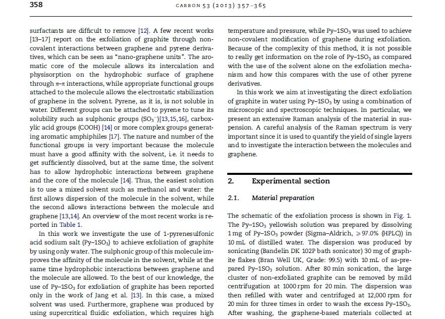
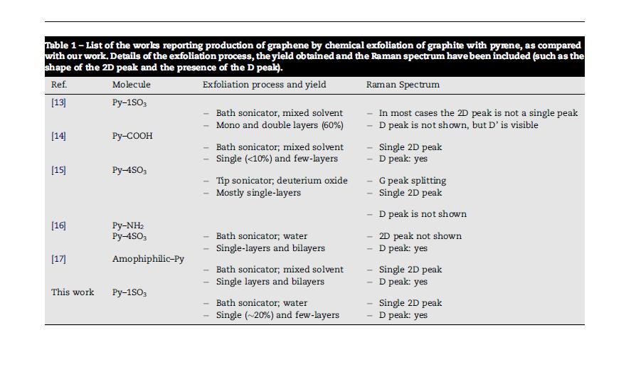
59 59
60 60
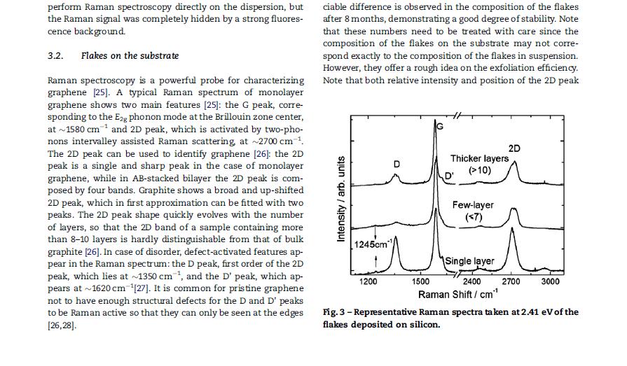
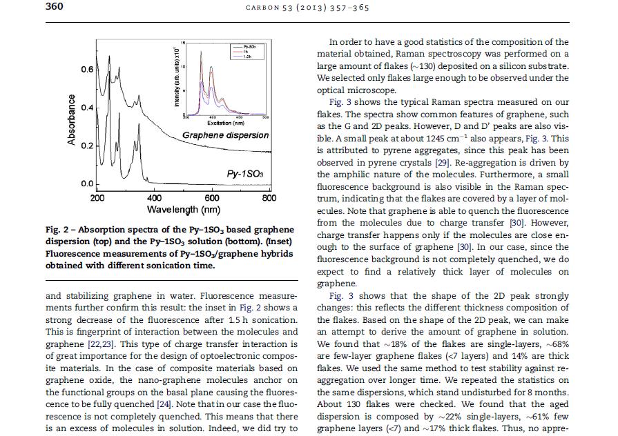
61 61
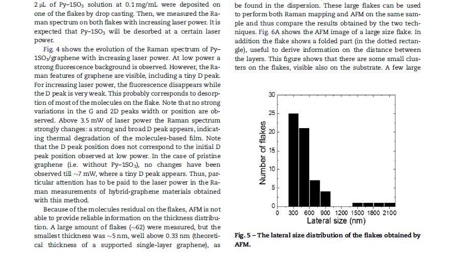
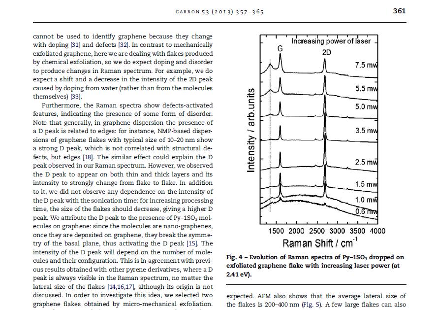
62 62
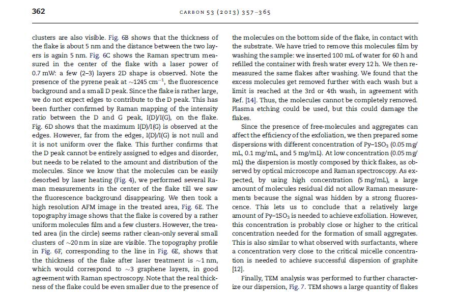
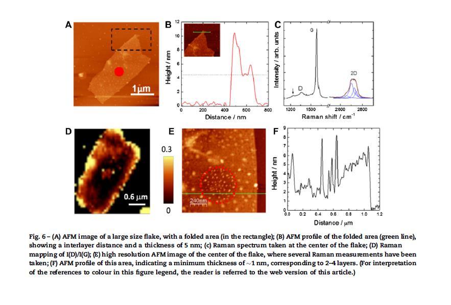
63 63
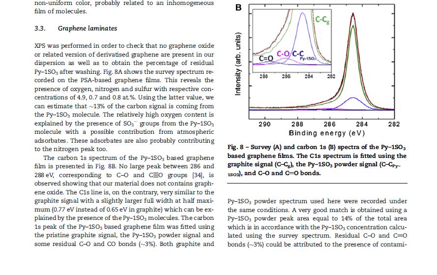
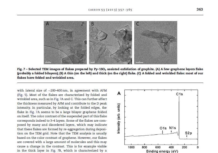
64 64
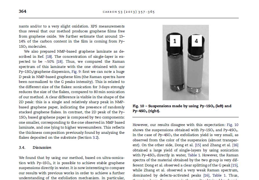
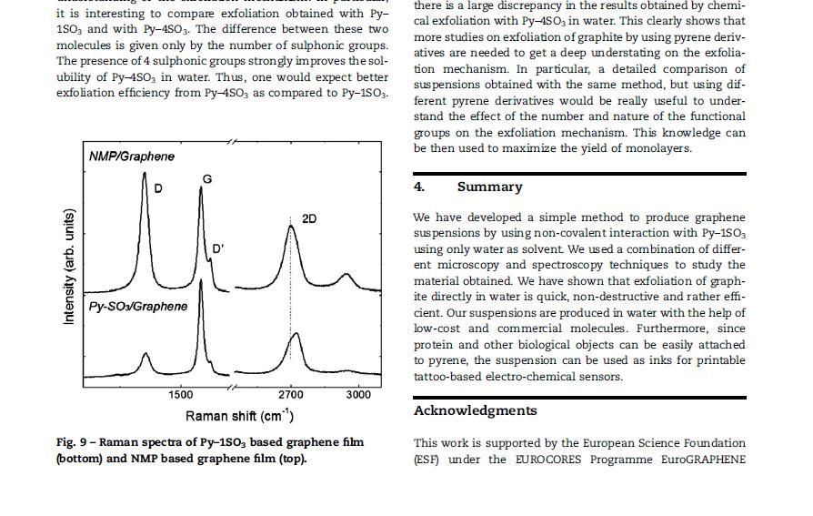
65 65
66 66
Graphene films on silicon carbide (SiC) wafers supplied by Nitride Crystals, Inc.
 wafers supplied by Nitride Crystals, Inc.") 9702 Gayton Road, Suite 320, Richmond, VA 23238, USA Phone: +1 (804) 709-6696 info@nitride-crystals.com www.nitride-crystals.com Graphene films on silicon carbide (SiC) wafers supplied by Nitride Crystals,
9702 Gayton Road, Suite 320, Richmond, VA 23238, USA Phone: +1 (804) 709-6696 info@nitride-crystals.com www.nitride-crystals.com Graphene films on silicon carbide (SiC) wafers supplied by Nitride Crystals,
Carbon based Nanoscale Electronics
 Carbon based Nanoscale Electronics 09 02 200802 2008 ME class Outline driving force for the carbon nanomaterial electronic properties of fullerene exploration of electronic carbon nanotube gold rush of
Graphene. Tianyu Ye November 30th, 2011
 Graphene Tianyu Ye November 30th, 2011 Outline What is graphene? How to make graphene? (Exfoliation, Epitaxial, CVD) Is it graphene? (Identification methods) Transport properties; Other properties; Applications;
Overview. Carbon in all its forms. Background & Discovery Fabrication. Important properties. Summary & References. Overview of current research
 Graphene Prepared for Solid State Physics II Pr Dagotto Spring 2009 Laurene Tetard 03/23/09 Overview Carbon in all its forms Background & Discovery Fabrication Important properties Overview of current
Monolayer Semiconductors
 Monolayer Semiconductors Gilbert Arias California State University San Bernardino University of Washington INT REU, 2013 Advisor: Xiaodong Xu (Dated: August 24, 2013) Abstract Silicon may be unable to
Wafer-scale fabrication of graphene
 Wafer-scale fabrication of graphene Sten Vollebregt, MSc Delft University of Technology, Delft Institute of Mircosystems and Nanotechnology Delft University of Technology Challenge the future Delft University
Initial Stages of Growth of Organic Semiconductors on Graphene
 Initial Stages of Growth of Organic Semiconductors on Graphene Presented by: Manisha Chhikara Supervisor: Prof. Dr. Gvido Bratina University of Nova Gorica Outline Introduction to Graphene Fabrication
Supplementary Figure S1. AFM images of GraNRs grown with standard growth process. Each of these pictures show GraNRs prepared independently,
 Supplementary Figure S1. AFM images of GraNRs grown with standard growth process. Each of these pictures show GraNRs prepared independently, suggesting that the results is reproducible. Supplementary Figure
SUPPLEMENTARY INFORMATION
 SUPPLEMENTARY INFORMATION Facile Synthesis of High Quality Graphene Nanoribbons Liying Jiao, Xinran Wang, Georgi Diankov, Hailiang Wang & Hongjie Dai* Supplementary Information 1. Photograph of graphene
CVD growth of Graphene. SPE ACCE presentation Carter Kittrell James M. Tour group September 9 to 11, 2014
 CVD growth of Graphene SPE ACCE presentation Carter Kittrell James M. Tour group September 9 to 11, 2014 Graphene zigzag armchair History 1500: Pencil-Is it made of lead? 1789: Graphite 1987: The first
Transparent Electrode Applications
 Transparent Electrode Applications LCD Solar Cells Touch Screen Indium Tin Oxide (ITO) Zinc Oxide (ZnO) - High conductivity - High transparency - Resistant to environmental effects - Rare material (Indium)
Supplementary Figure 1: Micromechanical cleavage of graphene on oxygen plasma treated Si/SiO2. Supplementary Figure 2: Comparison of hbn yield.
 1 2 3 4 Supplementary Figure 1: Micromechanical cleavage of graphene on oxygen plasma treated Si/SiO 2. Optical microscopy images of three examples of large single layer graphene flakes cleaved on a single
Carbon nanotubes in a nutshell. Graphite band structure. What is a carbon nanotube? Start by considering graphite.
 Carbon nanotubes in a nutshell What is a carbon nanotube? Start by considering graphite. sp 2 bonded carbon. Each atom connected to 3 neighbors w/ 120 degree bond angles. Hybridized π bonding across whole
Graphene The Search For Two Dimensions. Christopher Scott Friedline Arizona State University
 Graphene The Search For Two Dimensions Christopher Scott Friedline Arizona State University What Is Graphene? Single atomic layer of graphite arranged in a honeycomb crystal lattice Consists of sp 2 -bonded
CHAPTER 3. OPTICAL STUDIES ON SnS NANOPARTICLES
 42 CHAPTER 3 OPTICAL STUDIES ON SnS NANOPARTICLES 3.1 INTRODUCTION In recent years, considerable interest has been shown on semiconducting nanostructures owing to their enhanced optical and electrical
Fig. 1: Raman spectra of graphite and graphene. N indicates the number of layers of graphene. Ref. [1]
![Fig. 1: Raman spectra of graphite and graphene. N indicates the number of layers of graphene. Ref. [1]](/thumbs/90/102653942.jpg "Fig. 1: Raman spectra of graphite and graphene. N indicates the number of layers of graphene. Ref. [1]") Vibrational Properties of Graphene and Nanotubes: The Radial Breathing and High Energy Modes Presented for the Selected Topics Seminar by Pierce Munnelly 09/06/11 Supervised by Sebastian Heeg Abstract
Vibrational Properties of Graphene and Nanotubes: The Radial Breathing and High Energy Modes Presented for the Selected Topics Seminar by Pierce Munnelly 09/06/11 Supervised by Sebastian Heeg Abstract
Supplementary Figure 1 Dark-field optical images of as prepared PMMA-assisted transferred CVD graphene films on silicon substrates (a) and the one
 and the one") Supplementary Figure 1 Dark-field optical images of as prepared PMMA-assisted transferred CVD graphene films on silicon substrates (a) and the one after PBASE monolayer growth (b). 1 Supplementary Figure
Supplementary Figure 1 Dark-field optical images of as prepared PMMA-assisted transferred CVD graphene films on silicon substrates (a) and the one after PBASE monolayer growth (b). 1 Supplementary Figure
Introduction to Nanotechnology Chapter 5 Carbon Nanostructures Lecture 1
 Introduction to Nanotechnology Chapter 5 Carbon Nanostructures Lecture 1 ChiiDong Chen Institute of Physics, Academia Sinica chiidong@phys.sinica.edu.tw 02 27896766 Carbon contains 6 electrons: (1s) 2,
Conference Return Seminar- NANO2014,Moscow State University,Moscow,Russia Date: th July 2014
 Conference Return Seminar- NANO2014,Moscow State University,Moscow,Russia Date:13-1818 th July 2014 An electrochemical method for the synthesis of single and few layers graphene sheets for high temperature
Transient Photocurrent Measurements of Graphene Related Materials
 Transient Photocurrent Measurements of Graphene Related Materials P. Srinivasa Rao Mentor: Prof. dr. Gvido Bratina Laboratory of Organic Matter Physics University of Nova Gorica 1 Contents: 1. Electrical
FMM, 15 th Feb Simon Zihlmann
 FMM, 15 th Feb. 2013 Simon Zihlmann Outline Motivation Basics about graphene lattice and edges Introduction to Raman spectroscopy Scattering at the edge Polarization dependence Thermal rearrangement of
Graphene Fundamentals and Emergent Applications
 Graphene Fundamentals and Emergent Applications Jamie H. Warner Department of Materials University of Oxford Oxford, UK Franziska Schaffel Department of Materials University of Oxford Oxford, UK Alicja
REDUCED GRAPHITE OXIDE-INDIUM TIN OXIDE COMPOSITES FOR TRANSPARENT ELECTRODE USING SOLUTION PROCESS
 18 TH INTERNATIONAL CONFERENCE ON COMPOSITE MATERIALS REDUCED GRAPHITE OXIDE-INDIUM TIN OXIDE COMPOSITES FOR TRANSPARENT ELECTRODE USING SOLUTION PROCESS K. S. Choi, Y. Park, K-.C. Kwon, J. Kim, C. K.
Band-like transport in highly crystalline graphene films from
 Supplementary figures Title: Band-like transport in highly crystalline graphene films from defective graphene oxides R. Negishi 1,*, M. Akabori 2, T. Ito 3, Y. Watanabe 4 and Y. Kobayashi 1 1 Department
Introduction to Nanotechnology Chapter 5 Carbon Nanostructures Lecture 1
 Introduction to Nanotechnology Chapter 5 Carbon Nanostructures Lecture 1 ChiiDong Chen Institute of Physics, Academia Sinica chiidong@phys.sinica.edu.tw 02 27896766 Section 5.2.1 Nature of the Carbon Bond
Carbon nanotubes in a nutshell
 Carbon nanotubes in a nutshell What is a carbon nanotube? Start by considering graphite. sp 2 bonded carbon. Each atom connected to 3 neighbors w/ 120 degree bond angles. Hybridized π bonding across whole
Semiconductor Polymer
 Semiconductor Polymer Organic Semiconductor for Flexible Electronics Introduction: An organic semiconductor is an organic compound that possesses similar properties to inorganic semiconductors with hole
Practical 1P4 Energy Levels and Band Gaps
 Practical 1P4 Energy Levels and Band Gaps What you should learn from this practical Science This practical illustrates some of the points from the lecture course on Elementary Quantum Mechanics and Bonding
Solid Type of solid Type of particle Al(s) aluminium MgCl2 Magnesium chloride S8(s) sulfur
 aluminium MgCl2 Magnesium chloride S8(s) sulfur") QUESTION (2017:1) (iii) Sodium chloride, NaCl, is another compound that is excreted from the body in sweat. Use your knowledge of structure and bonding to explain the dissolving process of sodium chloride,
QUESTION (2017:1) (iii) Sodium chloride, NaCl, is another compound that is excreted from the body in sweat. Use your knowledge of structure and bonding to explain the dissolving process of sodium chloride,
Chapter 4: Bonding in Solids and Electronic Properties. Free electron theory
 Chapter 4: Bonding in Solids and Electronic Properties Free electron theory Consider free electrons in a metal an electron gas. regards a metal as a box in which electrons are free to move. assumes nuclei
GRAPHENE the first 2D crystal lattice
 GRAPHENE the first 2D crystal lattice dimensionality of carbon diamond, graphite GRAPHENE realized in 2004 (Novoselov, Science 306, 2004) carbon nanotubes fullerenes, buckyballs what s so special about
Supplementary Figure 1 Detailed illustration on the fabrication process of templatestripped
 Supplementary Figure 1 Detailed illustration on the fabrication process of templatestripped gold substrate. (a) Spin coating of hydrogen silsesquioxane (HSQ) resist onto the silicon substrate with a thickness
ELEMENTARY BAND THEORY
 ELEMENTARY BAND THEORY PHYSICIST Solid state band Valence band, VB Conduction band, CB Fermi energy, E F Bloch orbital, delocalized n-doping p-doping Band gap, E g Direct band gap Indirect band gap Phonon
Basic Semiconductor Physics
 6 Basic Semiconductor Physics 6.1 Introduction With this chapter we start with the discussion of some important concepts from semiconductor physics, which are required to understand the operation of solar
Graphene FETs EE439 FINAL PROJECT. Yiwen Meng Su Ai
 Graphene FETs EE439 FINAL PROJECT Yiwen Meng Su Ai Introduction What is Graphene? An atomic-scale honeycomb lattice made of carbon atoms Before 2004, Hypothetical Carbon Structure Until 2004, physicists
2D Materials for Gas Sensing
 2D Materials for Gas Sensing S. Guo, A. Rani, and M.E. Zaghloul Department of Electrical and Computer Engineering The George Washington University, Washington DC 20052 Outline Background Structures of
Supplementary Figure 1 Experimental setup for crystal growth. Schematic drawing of the experimental setup for C 8 -BTBT crystal growth.
 Supplementary Figure 1 Experimental setup for crystal growth. Schematic drawing of the experimental setup for C 8 -BTBT crystal growth. Supplementary Figure 2 AFM study of the C 8 -BTBT crystal growth
Graphene Based Saturable Absorber Modelockers at 2µm
 ISLA Workshop Munich Integrated disruptive components for 2µm fibre Lasers ISLA Graphene Based Saturable Absorber Modelockers at 2µm Prof. Werner Blau - Trinity College Dublin Friday, 26th of June 2015
3-month progress Report
 3-month progress Report Graphene Devices and Circuits Supervisor Dr. P.A Childs Table of Content Abstract... 1 1. Introduction... 1 1.1 Graphene gold rush... 1 1.2 Properties of graphene... 3 1.3 Semiconductor
STM and graphene. W. W. Larry Pai ( 白偉武 ) Center for condensed matter sciences, National Taiwan University NTHU, 2013/05/23
 Center for condensed matter sciences, National Taiwan University NTHU, 2013/05/23") STM and graphene W. W. Larry Pai ( 白偉武 ) Center for condensed matter sciences, National Taiwan University NTHU, 2013/05/23 Why graphene is important: It is a new form of material (two dimensional, single
STM and graphene W. W. Larry Pai ( 白偉武 ) Center for condensed matter sciences, National Taiwan University NTHU, 2013/05/23 Why graphene is important: It is a new form of material (two dimensional, single
Electron Energy, E E = 0. Free electron. 3s Band 2p Band Overlapping energy bands. 3p 3s 2p 2s. 2s Band. Electrons. 1s ATOM SOLID.
 Electron Energy, E Free electron Vacuum level 3p 3s 2p 2s 2s Band 3s Band 2p Band Overlapping energy bands Electrons E = 0 1s ATOM 1s SOLID In a metal the various energy bands overlap to give a single
Black phosphorus: A new bandgap tuning knob
 Black phosphorus: A new bandgap tuning knob Rafael Roldán and Andres Castellanos-Gomez Modern electronics rely on devices whose functionality can be adjusted by the end-user with an external knob. A new
Review of Optical Properties of Materials
 Review of Optical Properties of Materials Review of optics Absorption in semiconductors: qualitative discussion Derivation of Optical Absorption Coefficient in Direct Semiconductors Photons When dealing
Practical 1P4 Energy Levels and Band Gaps
 Practical 1P4 Energy Levels and Band Gaps What you should learn from this practical Science This practical illustrates some of the points from the lecture course on Elementary Quantum Mechanics and Bonding
Solutions for Assignment-8
 Solutions for Assignment-8 Q1. The process of adding impurities to a pure semiconductor is called: [1] (a) Mixing (b) Doping (c) Diffusing (d) None of the above In semiconductor production, doping intentionally
Supplementary Figure S1. AFM characterizations and topographical defects of h- BN films on silica substrates. (a) (c) show the AFM height
 (c) show the AFM height") Supplementary Figure S1. AFM characterizations and topographical defects of h- BN films on silica substrates. (a) (c) show the AFM height topographies of h-bn film in a size of ~1.5µm 1.5µm, 30µm 30µm
Supplementary Figure S1. AFM characterizations and topographical defects of h- BN films on silica substrates. (a) (c) show the AFM height topographies of h-bn film in a size of ~1.5µm 1.5µm, 30µm 30µm
2011 GCEP Report. Project title: Self-sorting of Carbon Nanotubes for High Performance Large Area Transparent Electrodes for Solar Cells
 2011 GCEP Report Project title: Self-sorting of Carbon Nanotubes for High Performance Large Area Transparent Electrodes for Solar Cells Investigators Zhenan Bao, Associate Professor, Chemical Engineering
Graphene Novel Material for Nanoelectronics
 Graphene Novel Material for Nanoelectronics Shintaro Sato Naoki Harada Daiyu Kondo Mari Ohfuchi (Manuscript received May 12, 2009) Graphene is a flat monolayer of carbon atoms with a two-dimensional honeycomb
The many forms of carbon
 The many forms of carbon Carbon is not only the basis of life, it also provides an enormous variety of structures for nanotechnology. This versatility is connected to the ability of carbon to form two
Electrons are shared in covalent bonds between atoms of Si. A bound electron has the lowest energy state.
 Photovoltaics Basic Steps the generation of light-generated carriers; the collection of the light-generated carriers to generate a current; the generation of a large voltage across the solar cell; and
Supplementary Figure 2 Photoluminescence in 1L- (black line) and 7L-MoS 2 (red line) of the Figure 1B with illuminated wavelength of 543 nm.
 and 7L-MoS 2 (red line) of the Figure 1B with illuminated wavelength of 543 nm.") PL (normalized) Intensity (arb. u.) 1 1 8 7L-MoS 1L-MoS 6 4 37 38 39 4 41 4 Raman shift (cm -1 ) Supplementary Figure 1 Raman spectra of the Figure 1B at the 1L-MoS area (black line) and 7L-MoS area (red
PL (normalized) Intensity (arb. u.) 1 1 8 7L-MoS 1L-MoS 6 4 37 38 39 4 41 4 Raman shift (cm -1 ) Supplementary Figure 1 Raman spectra of the Figure 1B at the 1L-MoS area (black line) and 7L-MoS area (red
Supplementary Information
 Supplementary Information Chemical and Bandgap Engineering in Monolayer Hexagonal Boron Nitride Kun Ba 1,, Wei Jiang 1,,Jingxin Cheng 2, Jingxian Bao 1, Ningning Xuan 1,Yangye Sun 1, Bing Liu 1, Aozhen
Low Voltage Field Emission SEM (LV FE-SEM): A Promising Imaging Approach for Graphene Samples
: A Promising Imaging Approach for Graphene Samples") Low Voltage Field Emission SEM (LV FE-SEM): A Promising Imaging Approach for Graphene Samples Jining Xie Agilent Technologies May 23 rd, 2012 www.agilent.com/find/nano Outline 1. Introduction 2. Agilent
Low Voltage Field Emission SEM (LV FE-SEM): A Promising Imaging Approach for Graphene Samples Jining Xie Agilent Technologies May 23 rd, 2012 www.agilent.com/find/nano Outline 1. Introduction 2. Agilent
A. Optimizing the growth conditions of large-scale graphene films
 1 A. Optimizing the growth conditions of large-scale graphene films Figure S1. Optical microscope images of graphene films transferred on 300 nm SiO 2 /Si substrates. a, Images of the graphene films grown
From Last Time. Several important conceptual aspects of quantum mechanics Indistinguishability. Symmetry
 From Last Time Several important conceptual aspects of quantum mechanics Indistinguishability particles are absolutely identical Leads to Pauli exclusion principle (one Fermion / quantum state). Symmetry
Energetic particles and their detection in situ (particle detectors) Part II. George Gloeckler
 Part II. George Gloeckler") Energetic particles and their detection in situ (particle detectors) Part II George Gloeckler University of Michigan, Ann Arbor, MI University of Maryland, College Park, MD Simple particle detectors Gas-filled
Energetic particles and their detection in situ (particle detectors) Part II George Gloeckler University of Michigan, Ann Arbor, MI University of Maryland, College Park, MD Simple particle detectors Gas-filled
III-V nanostructured materials synthesized by MBE droplet epitaxy
 III-V nanostructured materials synthesized by MBE droplet epitaxy E.A. Anyebe 1, C. C. Yu 1, Q. Zhuang 1,*, B. Robinson 1, O Kolosov 1, V. Fal ko 1, R. Young 1, M Hayne 1, A. Sanchez 2, D. Hynes 2, and
So why is sodium a metal? Tungsten Half-filled 5d band & half-filled 6s band. Insulators. Interaction of metals with light?
 Bonding in Solids: Metals, Insulators, & CHEM 107 T. Hughbanks Delocalized bonding in Solids Think of a pure solid as a single, very large molecule. Use our bonding pictures to try to understand properties.
The Raman Spectroscopy of Graphene and the Determination of Layer Thickness
 Application Note: 52252 The Raman Spectroscopy of Graphene and the Determination of Layer Thickness Mark Wall, Ph.D., Thermo Fisher Scientific, Madison, WI, USA Key Words DXR Raman Microscope 2D Band D
554 Chapter 10 Liquids and Solids
 554 Chapter 10 Liquids and Solids above 7376 kpa, CO 2 is a supercritical fluid, with properties of both gas and liquid. Like a gas, it penetrates deep into the coffee beans; like a liquid, it effectively
XPS Depth Profiling of Epitaxial Graphene Intercalated with FeCl 3
 XPS Depth Profiling of Epitaxial Graphene Intercalated with FeCl 3 Mahdi Ibrahim Maynard H. Jackson High School Atlanta, GA. Faculty Advisor: Dr. Kristin Shepperd Research Group: Prof. Edward Conrad School
Pin-Chun Shen M.S. Photonics and Optoelectronics National Taiwan University, 2014
 Large-area CVD Growth of Two-dimensional Transition Metal Dichalcogenides and Monolayer MoS 2 and WS 2 Metal oxide semiconductor Field-effect Transistors by Pin-Chun Shen M.S. Photonics and Optoelectronics
Production of Graphite Chloride and Bromide Using Microwave Sparks
 Supporting Information Production of Graphite Chloride and Bromide Using Microwave Sparks Jian Zheng, Hongtao Liu, Bin Wu, Chong-an Di, Yunlong Guo, Ti Wu, Gui Yu, Yunqi Liu, * and Daoben Zhu Key Laboratory
Lectures Graphene and
 Lectures 15-16 Graphene and carbon nanotubes Graphene is atomically thin crystal of carbon which is stronger than steel but flexible, is transparent for light, and conducts electricity (gapless semiconductor).
Supporting Information Available:
 Supporting Information Available: Photoresponsive and Gas Sensing Field-Effect Transistors based on Multilayer WS 2 Nanoflakes Nengjie Huo 1, Shengxue Yang 1, Zhongming Wei 2, Shu-Shen Li 1, Jian-Bai Xia
This manuscript was submitted first in a reputed journal on Apri1 16 th Stanene: Atomically Thick Free-standing Layer of 2D Hexagonal Tin
 This manuscript was submitted first in a reputed journal on Apri1 16 th 2015 Stanene: Atomically Thick Free-standing Layer of 2D Hexagonal Tin Sumit Saxena 1, Raghvendra Pratap Choudhary, and Shobha Shukla
Imaging Carbon materials with correlative Raman-SEM microscopy. Introduction. Raman, SEM and FIB within one chamber. Diamond.
 Imaging Carbon materials with correlative Raman-SEM microscopy Application Example Carbon materials are widely used in many industries for their exceptional properties. Electric conductance, light weight,
2D MBE Activities in Sheffield. I. Farrer, J. Heffernan Electronic and Electrical Engineering The University of Sheffield
 2D MBE Activities in Sheffield I. Farrer, J. Heffernan Electronic and Electrical Engineering The University of Sheffield Outline Motivation Van der Waals crystals The Transition Metal Di-Chalcogenides
Supplementary Figure 1. Electron micrographs of graphene and converted h-bn. (a) Low magnification STEM-ADF images of the graphene sample before
 Low magnification STEM-ADF images of the graphene sample before") Supplementary Figure 1. Electron micrographs of graphene and converted h-bn. (a) Low magnification STEM-ADF images of the graphene sample before conversion. Most of the graphene sample was folded after
Supplementary Figure 1. Electron micrographs of graphene and converted h-bn. (a) Low magnification STEM-ADF images of the graphene sample before conversion. Most of the graphene sample was folded after
Supporting Information
 Supporting Information Oh et al. 10.1073/pnas.0811923106 SI Text Hysteresis of BPE-PTCDI MW-TFTs. Fig. S9 represents bidirectional transfer plots at V DS 100VinN 2 atmosphere for transistors constructed
Session V: Graphene. Matteo Bruna CAMBRIDGE UNIVERSITY DEPARTMENT OF ENGINEERING
 Session V: Graphene Matteo Bruna Graphene: Material in the Flatland Graphite Graphene Properties: Thinnest imaginable material Good(and tunable) electrical conductor Strongest ever measured Stiffest known
Secondary Ion Mass Spectrometry (SIMS)
") CHEM53200: Lecture 10 Secondary Ion Mass Spectrometry (SIMS) Major reference: Surface Analysis Edited by J. C. Vickerman (1997). 1 Primary particles may be: Secondary particles can be e s, neutral species
CHEM53200: Lecture 10 Secondary Ion Mass Spectrometry (SIMS) Major reference: Surface Analysis Edited by J. C. Vickerman (1997). 1 Primary particles may be: Secondary particles can be e s, neutral species
Synthesis and Characterization of Exfoliated Graphite (EG) and to Use it as a Reinforcement in Zn-based Metal Matrix Composites
 and to Use it as a Reinforcement in Zn-based Metal Matrix Composites") Synthesis and Characterization of Exfoliated Graphite (EG) and to Use it as a Reinforcement in Zn-based Metal Matrix Composites Here H 2 SO 4 was used as an intercalant and H 2 O 2 as an oxidant. Expandable
Synthesis and Characterization of Exfoliated Graphite (EG) and to Use it as a Reinforcement in Zn-based Metal Matrix Composites Here H 2 SO 4 was used as an intercalant and H 2 O 2 as an oxidant. Expandable
CHEM Principles of Chemistry II Chapter 10 - Liquids and Solids
 CHEM 1212 - Principles of Chemistry II Chapter 10 - Liquids and Solids 10.1 Intermolecular Forces recall intramolecular (within the molecule) bonding whereby atoms can form stable units called molecules
Raman Imaging and Electronic Properties of Graphene
 Raman Imaging and Electronic Properties of Graphene F. Molitor, D. Graf, C. Stampfer, T. Ihn, and K. Ensslin Laboratory for Solid State Physics, ETH Zurich, 8093 Zurich, Switzerland ensslin@phys.ethz.ch
Classification of Solids
 Classification of Solids Classification by conductivity, which is related to the band structure: (Filled bands are shown dark; D(E) = Density of states) Class Electron Density Density of States D(E) Examples
Acoustic metamaterials in nanoscale
 Acoustic metamaterials in nanoscale Dr. Ari Salmi www.helsinki.fi/yliopisto 12.2.2014 1 Revisit to resonances Matemaattis-luonnontieteellinen tiedekunta / Henkilön nimi / Esityksen nimi www.helsinki.fi/yliopisto
Supplementary information. Derivatization and Interlaminar Debonding of Graphite-Iron Nanoparticles Hybrid
 Electronic Supplementary Material (ESI) for Physical Chemistry Chemical Physics. This journal is the Owner Societies 2017 Supplementary information Derivatization and Interlaminar Debonding of Graphite-Iron
UNIVERSITY OF CALIFORNIA College of Engineering Department of Electrical Engineering and Computer Sciences. Professor Ali Javey. Spring 2009.
 UNIVERSITY OF CALIFORNIA College of Engineering Department of Electrical Engineering and Computer Sciences EE143 Professor Ali Javey Spring 2009 Exam 1 Name: SID: Closed book. One sheet of notes is allowed.
Processing of Semiconducting Materials Prof. Pallab Banerji Department of Material Science Indian Institute of Technology, Kharagpur
 Processing of Semiconducting Materials Prof. Pallab Banerji Department of Material Science Indian Institute of Technology, Kharagpur Lecture - 4 Doping in Semiconductors Good morning. Let us start with
SUPPORTING INFORMATION
 Electronic Supplementary Material (ESI) for Nanoscale. This journal is The Royal Society of Chemistry 2014 SUPPORTING INFORMATION Materials Graphite powder (SP-1 graphite) was obtained from Bay carbon.
Chemistry Instrumental Analysis Lecture 8. Chem 4631
 Chemistry 4631 Instrumental Analysis Lecture 8 UV to IR Components of Optical Basic components of spectroscopic instruments: stable source of radiant energy transparent container to hold sample device
Supplementary Materials for
 advances.sciencemag.org/cgi/content/full/4/3/e1701373/dc1 Supplementary Materials for Atomically thin gallium layers from solid-melt exfoliation Vidya Kochat, Atanu Samanta, Yuan Zhang, Sanjit Bhowmick,
Chapter 4 Scintillation Detectors
 Med Phys 4RA3, 4RB3/6R03 Radioisotopes and Radiation Methodology 4-1 4.1. Basic principle of the scintillator Chapter 4 Scintillation Detectors Scintillator Light sensor Ionizing radiation Light (visible,
4. CV curve of GQD on platinum electrode S9
 Supporting Information Luminscent Graphene Quantum Dots (GQDs) for Organic Photovoltaic Devices Vinay Gupta*, Neeraj Chaudhary, Ritu Srivastava, Gauri Dutt Sharma, Ramil Bhardwaj, Suresh Chand National
Surface atoms/molecules of a material act as an interface to its surrounding environment;
 1 Chapter 1 Thesis Overview Surface atoms/molecules of a material act as an interface to its surrounding environment; their properties are often complicated by external adsorbates/species on the surface
Free Electron Model for Metals
 Free Electron Model for Metals Metals are very good at conducting both heat and electricity. A lattice of in a sea of electrons shared between all nuclei (moving freely between them): This is referred
Intensity (a.u.) Intensity (a.u.) Raman Shift (cm -1 ) Oxygen plasma. 6 cm. 9 cm. 1mm. Single-layer graphene sheet. 10mm. 14 cm
 Intensity (a.u.) Raman Shift (cm -1 ) Oxygen plasma. 6 cm. 9 cm. 1mm. Single-layer graphene sheet. 10mm. 14 cm") Intensity (a.u.) Intensity (a.u.) a Oxygen plasma b 6 cm 1mm 10mm Single-layer graphene sheet 14 cm 9 cm Flipped Si/SiO 2 Patterned chip Plasma-cleaned glass slides c d After 1 sec normal Oxygen plasma
Intensity (a.u.) Intensity (a.u.) a Oxygen plasma b 6 cm 1mm 10mm Single-layer graphene sheet 14 cm 9 cm Flipped Si/SiO 2 Patterned chip Plasma-cleaned glass slides c d After 1 sec normal Oxygen plasma
TRANSVERSE SPIN TRANSPORT IN GRAPHENE
 International Journal of Modern Physics B Vol. 23, Nos. 12 & 13 (2009) 2641 2646 World Scientific Publishing Company TRANSVERSE SPIN TRANSPORT IN GRAPHENE TARIQ M. G. MOHIUDDIN, A. A. ZHUKOV, D. C. ELIAS,
Introducing the RoVaCBE Flagship project: Roll-to-roll Vacuum-processed Carbon Based Electronics. Dr Hazel Assender, University of Oxford
 Introducing the RoVaCBE Flagship project: Roll-to-roll Vacuum-processed Carbon Based Electronics Dr Hazel Assender, University of Oxford DALMATIAN TECHNOLOGY 21 st Sept 2010 1 Organic electronics Opportunity
Supplementary information for Tunneling Spectroscopy of Graphene-Boron Nitride Heterostructures
 Supplementary information for Tunneling Spectroscopy of Graphene-Boron Nitride Heterostructures F. Amet, 1 J. R. Williams, 2 A. G. F. Garcia, 2 M. Yankowitz, 2 K.Watanabe, 3 T.Taniguchi, 3 and D. Goldhaber-Gordon
From Last Time Important new Quantum Mechanical Concepts. Atoms and Molecules. Today. Symmetry. Simple molecules.
 Today From Last Time Important new Quantum Mechanical Concepts Indistinguishability: Symmetries of the wavefunction: Symmetric and Antisymmetric Pauli exclusion principle: only one fermion per state Spin
UNIVERSITY OF CALIFORNIA College of Engineering Department of Electrical Engineering and Computer Sciences. Fall Exam 1
 UNIVERSITY OF CALIFORNIA College of Engineering Department of Electrical Engineering and Computer Sciences EECS 143 Fall 2008 Exam 1 Professor Ali Javey Answer Key Name: SID: 1337 Closed book. One sheet
Energy Spectroscopy. Ex.: Fe/MgO
 Energy Spectroscopy Spectroscopy gives access to the electronic properties (and thus chemistry, magnetism,..) of the investigated system with thickness dependence Ex.: Fe/MgO Fe O Mg Control of the oxidation
Physics of Nanotubes, Graphite and Graphene Mildred Dresselhaus
 Quantum Transport and Dynamics in Nanostructures The 4 th Windsor Summer School on Condensed Matter Theory 6-18 August 2007, Great Park Windsor (UK) Physics of Nanotubes, Graphite and Graphene Mildred
Graphene and Carbon Nanotubes
 Graphene and Carbon Nanotubes 1 atom thick films of graphite atomic chicken wire Novoselov et al - Science 306, 666 (004) 100μm Geim s group at Manchester Novoselov et al - Nature 438, 197 (005) Kim-Stormer
Minimal Update of Solid State Physics
 Minimal Update of Solid State Physics It is expected that participants are acquainted with basics of solid state physics. Therefore here we will refresh only those aspects, which are absolutely necessary
Unit IV Semiconductors Engineering Physics
 Introduction A semiconductor is a material that has a resistivity lies between that of a conductor and an insulator. The conductivity of a semiconductor material can be varied under an external electrical
Free Electron Model for Metals
 Free Electron Model for Metals Metals are very good at conducting both heat and electricity. A lattice of in a sea of electrons shared between all nuclei (moving freely between them): This is referred
Fabrication Technology, Part I
 EEL5225: Principles of MEMS Transducers (Fall 2004) Fabrication Technology, Part I Agenda: Microfabrication Overview Basic semiconductor devices Materials Key processes Oxidation Thin-film Deposition Reading: