Physics Research in Affiliated Areas
|
|
|
- Ronald Stewart
- 6 years ago
- Views:
Transcription

1 Physics Research in Affiliated Areas Quantum Optics, Biological Physics, Biomedical Optics, Ultramicroscopy, Device and Materials Physics Bennett Goldberg, PHY Shyam Erramilli PHY Alexander Sergienko ECE Ted Moustakas ECE Selim Ünlü ECE Luca Dal Negro ECE Irving Bigio BME Evan Evans BME Amit Meller BME Bahaa Saleh ECE Mal Teich ECE
 M. Booth J. Hofman Packard Y. Liu V. Lai CIPA M. Nasr B. O'Hare MIT LL M. Shaw A. Schwartz DARPA Quist K.")
2 QUANTUM IMAGING LABORATORY at Boston University CO-DIRECTORS: B. E. A. Saleh, A. V. Sergienko, M. C. Teich Postdocs Grad Students Undergrads Support G. Di Giuseppe A. Abouraddy M. Corbo NSF CenSSIS G. Jaeger M. Atatüre E. Dauler NSF (CCR, CISE, AMOP) M. Booth J. Hofman Packard Y. Liu V. Lai CIPA M. Nasr B. O'Hare MIT LL M. Shaw A. Schwartz DARPA Quist K. Toussaint NRO N. Vamivakas NIH Z. Walton BUPC T. Yarnall


3 Parametric Down Conversion - source of entangled states Phase Matching TYPE I Phase Matching TYPE II QuickTime and a Sorenson Video decompressor are needed to see this picture. QuickTime and a Sorenson Video decompressor are needed to see this picture. -Photons 1 and 2 have the same polarization and traverse the same direction -Photons 1 and 2 have orthogonal polarizations and travel different directions
4 Applications Quantum Information and Communication, Quantum Networking: multiparty secure quantum key distribution (quantum cryptography). (In cooperation with Tom Toffoli and Lev Levitin at BU). Quantum Imaging (Spatial Entanglement at Work): designing imaging configurations for unconventional practical applications. Quantum Ellipsometry: characterization of surface properties of semiconductors, and materials used in optoelectronics. Quantum Optical Tomography: (of real objects) do not confuse with tomography of quantum states. The feasibility of cryptography, metrology, and imaging has been demonstrated experimentally in our laboratory and experiments demonstrating ellipsometry, microscopy, tomography, and holography are underway.

5 Nanophotonics and Optical Characterization Ultramicroscopy Material Characterization Time-resolved spectroscopy Scanning probe microscopy NSOM, tip-enhanced Biological detection and sensing Thermal Imaging Photodetectors Resonant Raman from single Nanotubes M. Selim Ünlü, B. B. Goldberg Anna Swan DARPA, NSF, ONR, ARO


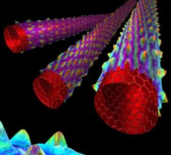
6 NANO OPTICS Carbon Nano-tubes Imaging of PBG, Waveguide Devices and Lasers High spatial resolution subsurface microscopy Quantum Dot Spectroscopy Goldberg & Ünlü
7 Resonant Raman scattering from Nanotube Raman scattering phonon m hω phonon photon E laser e,h photon E ± hω laser phonon Raman spectrum Intensity Phonon Absorption Anti-Stokes Phonon Emission Stokes E Shift Resonant Raman scattering incoming outgoing + hϖ phonon hϖ phonon Resonant Raman excitation profile incoming Stokes Eii Stokes E ii Raman Intensity Antistokes outgoing Anti- Stokes E ii E laser


 CVD")


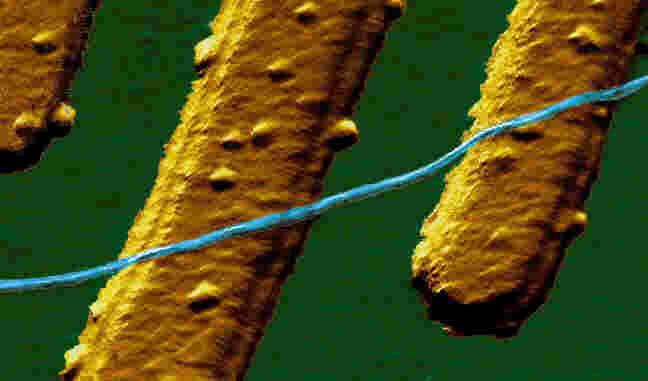
8 Resonant Raman Scattering Excitation (RRSE) of CNT (11,0) CVD growth Carbon nanotube suspended in trenches SEM 1-phonon: RBM 2-phonon: RBM 2


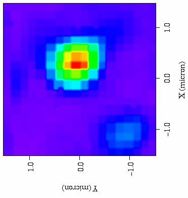
9 NAIL: Numerical Aperture Increasing Lens 100X objective Conventional State-of-the-art 10 µm 10X w/ NAIL Boston Univ.
 Carbon nanotubes: - well defined topography -large σ Raman - resonance")
10 SURFACE ENHANCED VIBRATIONAL SPECTROSCOPY AND MICROSCOPY ωo ωo + ωn ω N Phys.Rev.Lett. 90, (2003) Carbon nanotubes: - well defined topography -large σ Raman - resonance enhancement
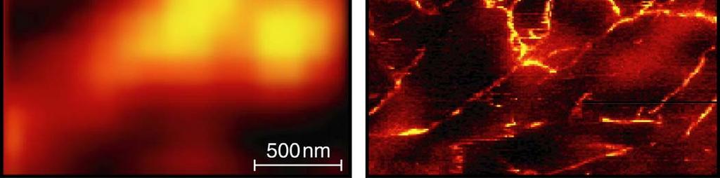
11 Comparison of Confocal to Tip-Enhanced in Raman Microscopy of Carbon nanotubes


 Myosin")


12 Molecules Organelles Cells Tissue Organs Organisms (meters) Myosin and kinesin motion on Actin fibers Shigella secretion system mutant 70nm wild type 35nm Science, Vol.300, 27 June 2003 Science, Vol.307, 25 February 2005
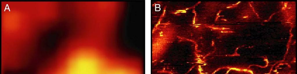
13 Spectral Self-interference Fluorescence Microscopy (SSFM) objective SiO Wavenumber, 1/λ (cm -1 )
14 Spectral Self-interference Fluorescence Microscopy (SSFM) objective SiO 2 10 nm Si Wavenumber, 1/λ (cm -1 ) INTENSITY QUENCHED SiO 2 spacer ~ 10nm~ /50
15 Spectral Self-interference Fluorescence Microscopy (SSFM) objective SiO 2 Si 250 nm ~ / Wavenumber, 1/λ (cm -1 ) INTENSITY ENHANCED SiO 2 spacer ~ 250nm~ /4
16 Spectral Self-interference Fluorescence Microscopy (SSFM) objective SiO 2 Si 2.5 µm ~ Wavenumber, 1/λ (cm -1 ) SPECTRAL VARIATIONS SiO 2 spacer ~ 2.5µm ~5
17 Spectral Self-interference Fluorescence Microscopy (SSFM) objective SiO 2 Si 5 µm ~ Wavenumber, 1/λ (cm -1 ) SPECTRAL VARIATIONS SiO 2 spacer ~ 5µm ~10

![labeled ) [nm] 14 12 10 8 6 4 2 0 0 5 10 15 frequency 50bp Double Strand DNA (Distal end labeled )](/docs-images/72/66446061/images/18-1.jpg "50 bp double strand DNA : 17 nm Measured average length : 10.5 nm 50 0 10.")
18 DNA Conformation Using SSFM Moiseev, L. et al, PNAS, vol.103,no. 8, February 21, 2006 Silane layer SiO 2 spacer Si substrate 50bp Double Strand DNA (Proximal end labeled ) [nm] frequency 50bp Double Strand DNA (Distal end labeled ) 50 bp double strand DNA : 17 nm Measured average length : 10.5 nm nm DNA as rigid rods on hinges Conclusion: Steric hindrance
19 Wide Bandgap Semiconductors Laboratory Theodore D. Moustakas In this laboratory we address materials and device physics issues of the wide bandgap semiconductors InN, GaN, AlN and their alloys and heterostructures. Current projects are related to making visible and ultraviolet LED and laser structures, solar-blind, UV photodetectors, electronic devices (diodes, transistors, thyristors) and MEMS sensors. The materials and devices are grown by molecular beam epitaxy (MBE), vapor phase epitaxy (VPE) and gas cluster ion-beam deposition (GCIB). Wide Bandgap Semiconductors Lab BOSTON UNIVERSITY
20 Bandgap-lattice constant Lattice Constant (Å) InN visible GaN ultraviolet AlN Bandgap Energy (ev) Wide Bandgap Semiconductors Lab BOSTON UNIVERSITY
21 Schematic of the ECR-MBE system N 2 purifier Compact ECR source RHEED gun Rotating heated wafer holder Beam flux monitor N 2 Transfer rod Shutter Group III: Ga, Al, In Dopants: Si, Mg Effusion cell RHEED screen Substrate Quadrupole mass spectrometer Buffer chamber Wide Bandgap Semiconductors Lab BOSTON UNIVERSITY


22 Laboratory for Nanometer Scale Mechanical Engineering Kamil L. Ekinci


23 Nanomechanics at BU Focus areas: 1. Surface analysis and engineering of nanostructures at the atomic scale 2. Nanoelectromechanical Systems (NEMS) sensors and signal processing components Experimental set up: UHV Surface analysis chamber High frequency NEMS Silicon atoms on the surface of a device


24 NEMS to measure single molecules Nanomechanical system moves nanometers at ultra high frequency => Sensitive to tiny amounts of material magnetomotive actuation and transduction single molecule detectors single molecule chemical sensors mass spectrometry Kamil Ekinci
25 Contacts and Information Near-field and Picosecond Spectroscopy: Quantum Imaging Laboratory: Biomedical Optics: Cellular and Subcellular Mechanics Lab: Semiconductor Device Research Lab:
26 Nanotechnology BOSTON UNIVERSITY Bennett Goldberg Electrical and Computer Engineering Physics selim@bu.edu goldberg@bu.edu

 Advanced E-beam")

 Optoelectronics")

27 Material Synthesis & Device Fabrication Nanomachining (Ekinci, Mech.ENG) Advanced E-beam lithography & surface micromachining (Mohanty, Physics) BioMEMS/NEMS (Desai and Tien, BME) Optoelectronics Processing Facility Lightwave Technology Laboratory III-V Nitride MBE (Moustakas, ECE) Ekinci, Moustakas, Mohanty

")
 = 68")

28 Applications in Biology and Biomedical Engineering : Nano-Bio-Technology 5 µm Nanoporous Silicon (psi) Particles Self Assembly of Scaffolds Volume (Particle) = 68 fl Volume (RBC) = fl High Resolution Biological Imaging Interdisciplinary Research Teams Desai & Tien
29 Center for Nanotechnology Integration CNI combines horizontal integration across disparate scientific disciplines vertical integration from basic science through transitional technologies to market opportunities Nanoscience and nanotechnology toward applications in human physiology Electronics/Photonics NEMS & MEMS Characterization Materials Science Nanofabrication Basic Science Tissue Engineering Smart Devices Manufacturing Biomimetic Materials Working from basic science through application engineering to device delivery New companies Understanding human Physiology Medical Applications Integrating scientists, engineers, medical doctors, entrepreneurs, and VC
30 NANOTECHNOLOGY Physical Sciences Life Sciences Electronics/Optics/IT Need Identified Enrico Belloti Thomas Bifano Kamil Ekinci Shymasunder Erramilli Bennett Goldberg Raj Mohanty Ted Morse Ted Moustakas Bahaa Saleh Anna Swan Selim Ünlü Energy Srikanth Gopalan Uday Pal Vinod Sarin Characterization Rama Bansil Bennett Goldberg Todd Murray Anna Swan Selim Ünlü Materials Science Kevin Smith Bennett Goldberg Karl Ludwig M. Selim Ünlü Ted Moustakas Manufacturing Thomas Bifano Tejal Desai Kamil Ekinci Raj Mohanty Andre Sharon Joe Tien Xin Zhang Homeland Security Bennett Goldberg Shymasunder Erramilli Raj Mohanty Ranjith Premisiri Selim Ünlü Smart Devices Thomas Bifano Irving Bigio Tejal Desai Kamil Ekinci Shymasunder Erramilli Evan Evans Maxim Frank-Kamenetski Rosina Georgiadis Bennett Goldberg Raj Mohanty Ted Morse Todd Murray Anna Swan Selim Ünlü Joyce Wong Xin Zhang Biology James Deshler Biomimetic Materials Tejal Desai Russell Giordano Catherine Klapperich Joe Tien Joyce Wong Xin Zhang Tissue Engineering Tejal Desai Evan Evans Russell Giordano Catherine Klapperich Joe Tien Joyce Wong Genomics & Proteomics Charles Cantor Jim Collins Michael Christman Charles Delisi Jim Deshler Shymasunder Erramilli Maxim Frank-Kamenetski Rosina Georgiadis Catherine Klapperich Cassandra Smith Zhiping Weng
31 Core Nanoscience efforts at Boston University Nano-optics in materials science Nanoscale Interdisciplinary Research Team developing optical techniques for at length scales of λ/10. NSF MURI with U of R Nano-optics in subcellular bioimaging and medicine Using new techniques in interference microscopy to image fluorophores in vivo with nanometer resolution. NIH+NSF Nano-electromechanical systems Nanosensor arrays for molecular detection using UHF cantelevers. NEMS for microengines, active mirrors, rapid and variable genomic and protein array fabrication Nano-electronics Nanowires, dots, and devices for coherent transport for secure communications and quantum computing Whitaker Laboratory for Micro and Nano Biosystems Nanotherapeutics: Targeted drug delivery, nanoporous membranes, smart nanoparticles Cellular scaffolding, polymer tethers 3D self assembly Nanomechanics of biosystems: Individual chemical bonds Dip-pen nanolithography, polymers Infrared microscopy to 100nm, femtogram spectroscopy and breast cancer screening using a single strand of hair Biosensing and homeland security Surface Plasmon Resonance, Array-based, multichannel sensors Ring resonators and fiber-based systems Proteomics and genomics
Nanomaterials and their Optical Applications
 Nanomaterials and their Optical Applications Winter Semester 2013 Lecture 02 rachel.grange@uni-jena.de http://www.iap.uni-jena.de/multiphoton Lecture 2: outline 2 Introduction to Nanophotonics Theoretical
Seminars in Nanosystems - I
 Seminars in Nanosystems - I Winter Semester 2011/2012 Dr. Emanuela Margapoti Emanuela.Margapoti@wsi.tum.de Dr. Gregor Koblmüller Gregor.Koblmueller@wsi.tum.de Seminar Room at ZNN 1 floor Topics of the
OPTICAL PROPERTIES AND SPECTROSCOPY OF NANOAAATERIALS. Jin Zhong Zhang. World Scientific TECHNISCHE INFORMATIONSBIBLIOTHEK
 OPTICAL PROPERTIES AND SPECTROSCOPY OF NANOAAATERIALS Jin Zhong Zhang University of California, Santa Cruz, USA TECHNISCHE INFORMATIONSBIBLIOTHEK Y World Scientific NEW JERSEY. t'on.don SINGAPORE «'BEIJING
Quantum Optical Coherence Tomography
 Quantum Optical Coherence Tomography Bahaa Saleh Alexander Sergienko Malvin Teich Quantum Imaging Lab Department of Electrical & Computer Engineering & Photonics Center QuickTime and a TIFF (Uncompressed)
Optical Spectroscopies of Thin Films and Interfaces. Dietrich R. T. Zahn Institut für Physik, Technische Universität Chemnitz, Germany
 Optical Spectroscopies of Thin Films and Interfaces Dietrich R. T. Zahn Institut für Physik, Technische Universität Chemnitz, Germany 1. Introduction 2. Vibrational Spectroscopies (Raman and Infrared)
2D Materials Research Activities at the NEST lab in Pisa, Italy. Stefan Heun NEST, Istituto Nanoscienze-CNR and Scuola Normale Superiore, Pisa, Italy
 2D Materials Research Activities at the NEST lab in Pisa, Italy Stefan Heun NEST, Istituto Nanoscienze-CNR and Scuola Normale Superiore, Pisa, Italy 2D Materials Research Activities at the NEST lab in
Nanotechnology? Source: National Science Foundation (NSF), USA
, USA") 2 2 Nanotechnology? Ability to work at the atomic, molecular and even sub-molecular levels in order to create and use material structures, devices and systems with new properties and functions Source:
2 2 Nanotechnology? Ability to work at the atomic, molecular and even sub-molecular levels in order to create and use material structures, devices and systems with new properties and functions Source:
What do we study and do?
 What do we study and do? Light comes from electrons transitioning from higher energy to lower energy levels. Wave-particle nature of light Wave nature: refraction, diffraction, interference (labs) Particle
Current and Emergent Developments
 Self Assembly and Biologically Inspired Processes in Applied Nanotechnology: Current and Emergent Developments Charles Ostman VP, Electronics & Photonics Forum chair NanoSig Senior Consultant Silicon Valley
Fundamentals of nanoscience
 Fundamentals of nanoscience Spectroscopy of nano-objects Mika Pettersson 1. Non-spatially resolved spectroscopy Traditionally, in spectroscopy, one is interested in obtaining information on the energy
Physics and Material Science of Semiconductor Nanostructures
 Physics and Material Science of Semiconductor Nanostructures PHYS 570P Prof. Oana Malis Email: omalis@purdue.edu Course website: http://www.physics.purdue.edu/academic_programs/courses/phys570p/ 1 Course
Fabrication at the nanoscale for nanophotonics
 Fabrication at the nanoscale for nanophotonics Ilya Sychugov, KTH Materials Physics, Kista silicon nanocrystal by electron beam induced deposition lithography Outline of basic nanofabrication methods Devices
ESH Benign Processes for he Integration of Quantum Dots (QDs)
") ESH Benign Processes for he Integration of Quantum Dots (QDs) PIs: Karen K. Gleason, Department of Chemical Engineering, MIT Graduate Students: Chia-Hua Lee: PhD Candidate, Department of Material Science
ESH Benign Processes for he Integration of Quantum Dots (QDs) PIs: Karen K. Gleason, Department of Chemical Engineering, MIT Graduate Students: Chia-Hua Lee: PhD Candidate, Department of Material Science
Other SPM Techniques. Scanning Probe Microscopy HT10
 Other SPM Techniques Scanning Near-Field Optical Microscopy (SNOM) Scanning Capacitance Microscopy (SCM) Scanning Spreading Resistance Microscopy (SSRM) Multiprobe techniques Electrostatic Force Microscopy,
GeSi Quantum Dot Superlattices
 GeSi Quantum Dot Superlattices ECE440 Nanoelectronics Zheng Yang Department of Electrical & Computer Engineering University of Illinois at Chicago Nanostructures & Dimensionality Bulk Quantum Walls Quantum
NANOCOMPOSITE THIN FILMS:
 NANOCOMPOSITE THIN FILMS: Assembly, Characterizations, & Applications Chaoyang Jiang Department of Chemistry The University of South Dakota St. Louis, June 26, 2008 Forest Products &Nanocomposite P. Monteiro@UC
Novel Nanoparticles for Ultrasensitive Detection and Spectroscopy
 Final Technical Report (DOE-FG02-98ER14873) Project Officer: Dr. Richard Gordon / Dr. John Miller Novel Nanoparticles for Ultrasensitive Detection and Spectroscopy Shuming Nie Indiana University P. 0.
1. Nanotechnology & nanomaterials -- Functional nanomaterials enabled by nanotechnologies.
 Novel Nano-Engineered Semiconductors for Possible Photon Sources and Detectors NAI-CHANG YEH Department of Physics, California Institute of Technology 1. Nanotechnology & nanomaterials -- Functional nanomaterials
Special Topics in Semiconductor Nanotechnology ECE 598XL
 Special Topics in Semiconductor Nanotechnology ECE 598XL Fall 2009 ECE 598XL Syllabus Overview: size matters Formation Process Characterization SOA device applications and potentials Homework or quizzes
Center for Integrated Nanotechnologies (CINT) Bob Hwang Co-Director, Sandia National Laboratories
 Bob Hwang Co-Director, Sandia National Laboratories") Center for Integrated Nanotechnologies (CINT) Bob Hwang Co-Director, Sandia National Laboratories Department of Energy Nanoscience Centers Molecular Foundry Center for Nanoscale Materials Center for Functional
Center for Integrated Nanotechnologies (CINT) Bob Hwang Co-Director, Sandia National Laboratories Department of Energy Nanoscience Centers Molecular Foundry Center for Nanoscale Materials Center for Functional
Self-Assembled InAs Quantum Dots
 Self-Assembled InAs Quantum Dots Steve Lyon Department of Electrical Engineering What are semiconductors What are semiconductor quantum dots How do we make (grow) InAs dots What are some of the properties
29: Nanotechnology. What is Nanotechnology? Properties Control and Understanding. Nanomaterials
 29: Nanotechnology What is Nanotechnology? Properties Control and Understanding Nanomaterials Making nanomaterials Seeing at the nanoscale Quantum Dots Carbon Nanotubes Biology at the Nanoscale Some Applications
Strong Coupling between On Chip Notched Ring Resonator and Nanoparticle
 Strong Coupling between On Chip Notched Ring Resonator and Nanoparticle S. Wang 1, K. Broderick 1, 3, H. Smith 1 2, 3,1 *, and Y. Yi 1 Massauchusetts Institute of Technology, Cambridge, MA 02139 2 New
Laser and Plasma-based Nanotechnologies
 Simpozionul: De la excelenta la competitivitate: tehnologiile generice esentiale Aula Academiei Romane, Bucuresti 15 mai 2014. Laser and Plasma-based Nanotechnologies Marian ZAMFIRESCU National Institute
Kavli Workshop for Journalists. June 13th, CNF Cleanroom Activities
 Kavli Workshop for Journalists June 13th, 2007 CNF Cleanroom Activities Seeing nm-sized Objects with an SEM Lab experience: Scanning Electron Microscopy Equipment: Zeiss Supra 55VP Scanning electron microscopes
Photonic Crystal Nanocavities for Efficient Light Confinement and Emission
 Journal of the Korean Physical Society, Vol. 42, No., February 2003, pp. 768 773 Photonic Crystal Nanocavities for Efficient Light Confinement and Emission Axel Scherer, T. Yoshie, M. Lončar, J. Vučković
Electrochemically Synthesized Multi-block
 Electrochemically Synthesized Multi-block Nanorods Sungho Park SungKyunKwan University, Department of Chemistry & SKKU Advanced Institute of Nanotechnology (SAINT) J. Am. Chem. Soc. 2003, 125, 2282-2290
RAJASTHAN TECHNICAL UNIVERSITY, KOTA
 RAJASTHAN TECHNICAL UNIVERSITY, KOTA (Electronics & Communication) Submitted By: LAKSHIKA SOMANI E&C II yr, IV sem. Session: 2007-08 Department of Electronics & Communication Geetanjali Institute of Technical
Nanotechnology where size matters
 Nanotechnology where size matters J Emyr Macdonald Overview Ways of seeing very small things What is nanotechnology and why is it important? Building nanostructures What we can do with nanotechnology?
There s plenty of room at the bottom! - R.P. Feynman, Nanostructure: a piece of material with at least one dimension less than 100 nm in extent.
 Nanostructures and Nanotechnology There s plenty of room at the bottom! - R.P. Feynman, 1959 Materials behave differently when structured at the nm scale than they do in bulk. Technologies now exist that
Microfabricação em materiais poliméricos usando laser de femtossegundos
 Microfabricação em materiais poliméricos usando laser de femtossegundos Prof. Cleber R. Mendonça http://www.fotonica.ifsc.usp.br University of Sao Paulo - Brazil students 77.000 52.000 undergrad. 25.000
Physicists in the Semiconductor Industry
 Physicists in the Semiconductor Industry P.M. Mooney IBM Research Division, T.J. Watson Research Center Yorktown Heights, NY 10598 APS March Meeting March 24, 2004 Thomas J. Watson Research Center 1 Outline
Sensing: a unified perspective for integrated photonics
 Sensing: a unified perspective for integrated photonics Chemical detection Environmental monitoring Process control Warfighter protection Biological sensing Drug discovery Food safety Medical diagnosis
Physics Open House Boston University Physics Department
 2012 Boston University Physics Department What are the Big Questions? Dept. of Energy BESAC Report (2007): Directing Boston UniversityMatter Slideshow Title and Goes Energy: Here Five Challenges for Science
Nanophysics: Main trends
 Nano-opto-electronics Nanophysics: Main trends Nanomechanics Main issues Light interaction with small structures Molecules Nanoparticles (semiconductor and metallic) Microparticles Photonic crystals Nanoplasmonics
ADVANCED ANALYTICAL LABORATORY
 An Information Brochure on ADVANCED ANALYTICAL LABORATORY ANDHRA UNIVERSITY Visakhapatnam - 530 003 Andhra Pradesh, India Sponsored by DEPARTMENT OF SCIENCE & TECHNOLOGY Government of India New Delhi 110016
Multiphoton Imaging and Spectroscopy in Cell and Tissue Biophysics. J Moger and C P Winlove
 Multiphoton Imaging and Spectroscopy in Cell and Tissue Biophysics J Moger and C P Winlove Relating Structure to Function Biochemistry Raman microspectrometry Surface enhanced Raman spectrometry (SERS)
Improving Micro-Raman/AFM Systems Imaging Using Negative-Stiffness Vibration Isolation
 Photonics.com - February 2011 Improving Micro-Raman/AFM Systems Imaging Using Negative-Stiffness Vibration Isolation Negative-stiffness vibration isolators can easily support the heavy weight of a combined
Course file PPY15204 Nanoscience and Nanomaterials Table of Contents
 Department Physics Nanotechnology : M.sc Physics Course file PPY15204 Table Contents Second Year MSc Physics (2015-2016 Regulation) Detailed Lesson Plan UNIT-I: INTRODUCTION TO NANOTECHNOLOGY History Importance
ME 4875/MTE C16. Introduction to Nanomaterials and Nanotechnology. Lecture 2 - Applications of Nanomaterials + Projects
 ME 4875/MTE 575 - C16 Introduction to Nanomaterials and Nanotechnology Lecture 2 - Applications of Nanomaterials + Projects 1 Project Teams of 4 students each Literature review of one application of nanotechnology
NANOMEDICINE. WILEY A John Wiley and Sons, Ltd., Publication DESIGN AND APPLICATIONS OF MAGNETIC NANOMATERIALS, NANOSENSORS AND NANOSYSTEMS
 NANOMEDICINE DESIGN AND APPLICATIONS OF MAGNETIC NANOMATERIALS, NANOSENSORS AND NANOSYSTEMS Vijay K. Varadan Linfeng Chen Jining Xie WILEY A John Wiley and Sons, Ltd., Publication Preface About the Authors
There's Plenty of Room at the Bottom
 There's Plenty of Room at the Bottom 12/29/1959 Feynman asked why not put the entire Encyclopedia Britannica (24 volumes) on a pin head (requires atomic scale recording). He proposed to use electron microscope
672 Advanced Solid State Physics. Scanning Tunneling Microscopy
 672 Advanced Solid State Physics Scanning Tunneling Microscopy Biao Hu Outline: 1. Introduction to STM 2. STM principle & working modes 3. STM application & extension 4. STM in our group 1. Introduction
Novel materials and nanostructures for advanced optoelectronics
 Novel materials and nanostructures for advanced optoelectronics Q. Zhuang, P. Carrington, M. Hayne, A Krier Physics Department, Lancaster University, UK u Brief introduction to Outline Lancaster University
Scattering-type near-field microscopy for nanoscale optical imaging
 Scattering-type near-field microscopy for nanoscale optical imaging Rainer Hillenbrand Nano-Photonics Group Max-Planck-Institut für Biochemie 82152 Martinsried, Germany Infrared light enables label-free
Applications of Terahertz Radiation (T-ray) Yao-Chang Lee, National Synchrotron Research Radiation Center
 Yao-Chang Lee, National Synchrotron Research Radiation Center") Applications of Terahertz Radiation (T-ray) Yao-Chang Lee, yclee@nsrrc.org.tw National Synchrotron Research Radiation Center Outline Terahertz radiation (THz) or T-ray The Interaction between T-ray and
Applications of Terahertz Radiation (T-ray) Yao-Chang Lee, yclee@nsrrc.org.tw National Synchrotron Research Radiation Center Outline Terahertz radiation (THz) or T-ray The Interaction between T-ray and
CURRICULUM VITAE. 1. To apply the knowledge which I learned theoretically in the practical setting.
 CURRICULUM VITAE II M,Sc. Nano Science and Technology, Coimbatore-641 046, Tamil Nadu. Mobile: +91-9843858762 E mail: maninano@gmail.com MANIVEL.P Objectives: 1. To apply the knowledge which I learned
OPTI510R: Photonics. Khanh Kieu College of Optical Sciences, University of Arizona Meinel building R.626
 OPTI510R: Photonics Khanh Kieu College of Optical Sciences, University of Arizona kkieu@optics.arizona.edu Meinel building R.626 Announcements HW #6 is assigned, due April 23 rd Final exam May 2 Semiconductor
Improving nano-scale imaging of of intergrated micro-raman/afm systems using negativestiffness
 See vibration isolation technology @ www.minusk.com?pdf) Electronic Products and Technology - May 2014 Improving nano-scale imaging of of intergrated micro-raman/afm systems using negativestiffness vibration
Lecture 1. Introduction to Electronic Materials. Reading: Pierret 1.1, 1.2, 1.4,
 Lecture 1 Introduction to Electronic Materials Reading: Pierret 1.1, 1.2, 1.4, 2.1-2.6 Atoms to Operational Amplifiers The goal of this course is to teach the fundamentals of non-linear circuit elements
Dip-Pen Lithography 1
 Dip-Pen Lithography 1 A Brief History of Writing Instruments From Quills and Bamboos to fountain pens and brushes M. Klein and Henry W. Wynne received US patent #68445 in 1867 for an ink chamber and delivery
Nanotechnology: Today and tomorrow
 Nanotechnology: Today and tomorrow Horst-Günter Rubahn NanoSYD Mads Clausen Instituttet Syddansk Universitet Alsion 2 6400 Sønderborg Agenda Alsion A bit about nano Nanoproducts Top down vs. bottom up
The Use of Synchrotron Radiation in Modern Research
 The Use of Synchrotron Radiation in Modern Research Physics Chemistry Structural Biology Materials Science Geochemical and Environmental Science Atoms, molecules, liquids, solids. Electronic and geometric
Chip-Scale Mass Spectrometers for Portable Gas Analyzers Luis Fernando Velásquez-García. A. I. Akinwande, K. Cheung, and L.-Y Chen.
 Chip-Scale Mass Spectrometers for Portable Gas Analyzers Luis Fernando Velásquez-García. A. I. Akinwande, K. Cheung, and L.-Y Chen. Microsystems Technology Laboratories (MTL) lfvelasq@mit.edu November
İZMİR INSTITUTE OF TECHNOLOGY GRADUATE SCHOOL OF ENGINEERING AND SCIENCES DEPARTMENT OF PHOTONICS SCIENCE AND ENGINEERING CURRICULUM OF THE
 GRADUATE SCHOOL OF AND SCIENCES DEPARTMENT OF PHOTONICS SCIENCE AND The Photonics Science and Engineering PhD Program is a jointly operated interdisciplinary program. The Curriculum is supported by the
Near-Infrared Spectroscopy of Nitride Heterostructures EMILY FINAN ADVISOR: DR. OANA MALIS PURDUE UNIVERSITY REU PROGRAM AUGUST 2, 2012
 Near-Infrared Spectroscopy of Nitride Heterostructures EMILY FINAN ADVISOR: DR. OANA MALIS PURDUE UNIVERSITY REU PROGRAM AUGUST 2, 2012 Introduction Experimental Condensed Matter Research Study of large
Quantum Technologies CCEM Workshop March 23 rd, 2017
 Quantum Technologies CCEM Workshop March 23 rd, 2017 JT Janssen Welcome to the National Physical Laboratory The first quantum revolution h V n f 2 e 1 The second quantum revolution Superposition Entanglement
Technology, Techniques and Applications. Ric Allott Business Development Manager
 Technology, Techniques and Applications Ric Allott Business Development Manager 1 Central Laser Facility ASTRA GEMINI VULCAN ARTEMIS ULTRA OCTOPUS High power, ultrashort pulse dual beams of 15 J, 30 fs
Nanoscale optical circuits: controlling light using localized surface plasmon resonances
 Nanoscale optical circuits: controlling light using localized surface plasmon resonances T. J. Davis, D. E. Gómez and K. C. Vernon CSIRO Materials Science and Engineering Localized surface plasmon (LSP)
Spring 2009 EE 710: Nanoscience and Engineering
 Spring 2009 EE 710: Nanoscience and Engineering Part 1: Introduction Course Texts: Bhushan, Springer Handbook of Nanotechnology 2 nd ed., Springer 2007 Hornyak, et.al, Introduction ti to Nanoscience, CRC
Fabrication / Synthesis Techniques
 Quantum Dots Physical properties Fabrication / Synthesis Techniques Applications Handbook of Nanoscience, Engineering, and Technology Ch.13.3 L. Kouwenhoven and C. Marcus, Physics World, June 1998, p.35
NEM Relays Using 2-Dimensional Nanomaterials for Low Energy Contacts
 NEM Relays Using 2-Dimensional Nanomaterials for Low Energy Contacts Seunghyun Lee, Ji Cao 10/29/2013 A Science & Technology Professor H. -S. Philip Wong Electrical Engineering, Stanford University Center
Nanoscale Heat Transfer and Information Technology
 Response to K.E. Goodson Nanoscale Heat Transfer and Information Technology Gang Chen Mechanical Engineering Department Massachusetts Institute of Technology Cambridge, MA 02139 Rohsenow Symposium on Future
Chapter 10. Nanometrology. Oxford University Press All rights reserved.
 Chapter 10 Nanometrology Oxford University Press 2013. All rights reserved. 1 Introduction Nanometrology is the science of measurement at the nanoscale level. Figure illustrates where nanoscale stands
In the name of Allah
 In the name of Allah Nano chemistry- 4 th stage Lecture No. 1 History of nanotechnology 16-10-2016 Assistance prof. Dr. Luma Majeed Ahmed lumamajeed2013@gmail.com, luma.ahmed@uokerbala.edu.iq Nano chemistry-4
DMR Support for National User Facilities and Major Instrumentation Projects
 DMR Support for National User Facilities and Major Instrumentation Projects Solid State Sciences Committee The National Academies, Washington, DC 6 April 2006 W. Lance Haworth Acting Director, Division
Currently, worldwide major semiconductor alloy epitaxial growth is divided into two material groups.
 ICQNM 2014 Currently, worldwide major semiconductor alloy epitaxial growth is divided into two material groups. Cubic: Diamond structures: group IV semiconductors (Si, Ge, C), Cubic zinc-blende structures:
Nano-mechatronics. Presented by: György BudaváriSzabó (X0LY4M)
") Nano-mechatronics Presented by: György BudaváriSzabó (X0LY4M) Nano-mechatronics Nano-mechatronics is currently used in broader spectra, ranging from basic applications in robotics, actuators, sensors,
Nano-mechatronics Presented by: György BudaváriSzabó (X0LY4M) Nano-mechatronics Nano-mechatronics is currently used in broader spectra, ranging from basic applications in robotics, actuators, sensors,
Putting quantum dot lasers to practical use
 Enviroment Life Nanotechnology Information Science Reconstruction Others Science and and Technology andfrom Energy Communications andthe Materials for Great Society EastTechnology Japan Earthquake (FY2017
Carbon Nanotube: Property, application and ultrafast optical spectroscopy
 Carbon Nanotube: Property, application and ultrafast optical spectroscopy Yijing Fu 1, Qing Yu 1 Institute of Optics, University of Rochester Department of Electrical engineering, University of Rochester
SUPPLEMENTARY INFORMATION
 SUPPLEMENTARY INFORMATION Phonon populations and electrical power dissipation in carbon nanotube transistors Supplemental Information Mathias Steiner 1, Marcus Freitag 1, Vasili Perebeinos 1, James C.
Quantum Dots for Advanced Research and Devices
 Quantum Dots for Advanced Research and Devices spectral region from 450 to 630 nm Zero-D Perovskite Emit light at 520 nm ABOUT QUANTUM SOLUTIONS QUANTUM SOLUTIONS company is an expert in the synthesis
Nanoscale Chemical Characterization: Moving to 3 Dimensions
 Nanoscale Chemical Characterization: Moving to 3 Dimensions Eric B. Steel Chemical Science & Technology Laboratory National Institute of Standards & Technology Outline What is and why do we need chemical
Near-Field Nano/Atom Optics and Technology
 M. Ohtsu (Ed.) Near-Field Nano/Atom Optics and Technology With 189 Figures / Springer Preface List of Contributors V VII XIII 1. Introduction 1 1.1 Near-Field Optics and Related Technologies 1 1.2 History
Nanosphere Lithography
 Nanosphere Lithography Derec Ciafre 1, Lingyun Miao 2, and Keita Oka 1 1 Institute of Optics / 2 ECE Dept. University of Rochester Abstract Nanosphere Lithography is quickly emerging as an efficient, low
Nanoscale confinement of photon and electron
 Nanoscale confinement of photon and electron Photons can be confined via: Planar waveguides or microcavities (2 d) Optical fibers (1 d) Micro/nano spheres (0 d) Electrons can be confined via: Quantum well
Optical imaging of metallic and semiconductor nanostructures at sub wavelength regime
 Optical imaging of metallic and semiconductor nanostructures at sub wavelength regime A. K. Sivadasan 1, Kishore K. Madapu 1 and Prajit Dhara 2 1 Nanomaterials Characterization and Sensors Section, Surface
Nanomaterials and Analytics Semiconductor Nanocrystals and Carbon Nanotubes. - Introduction and Preparation - Characterisation - Applications
 Nanomaterials and Analytics Semiconductor Nanocrystals and Carbon Nanotubes - Introduction and Preparation - Characterisation - Applications Dietrich RT Zahn Semiconductor Physics,, TU Chemnitz http://www.tu-chemnitz.de/physik/hlph/
( It will be applied from Fall)
") İZMİR INSTITUTE OF TECHNOLOGY GRADUATE SCHOOL OF ENGINEERING AND SCIENCES DEPARTMENT OF PHOTONICS SCIENCE AND ENGINEERING CURRICULUM OF THE MS PROGRAM IN PHOTONICS SCIENCE AND ENGINEERING The Photonics
İZMİR INSTITUTE OF TECHNOLOGY GRADUATE SCHOOL OF ENGINEERING AND SCIENCES DEPARTMENT OF PHOTONICS SCIENCE AND ENGINEERING CURRICULUM OF THE MS PROGRAM IN PHOTONICS SCIENCE AND ENGINEERING The Photonics
Reducing dimension. Crystalline structures
 Reducing dimension 2D surfaces, interfaces and quantum wells 1D carbon nanotubes, quantum wires and conducting polymers 0D nanocrystals, nanoparticles, lithographically patterned quantum dots Crystalline
Università degli Studi di Bari "Aldo Moro"
 Università degli Studi di Bari "Aldo Moro" Table of contents 1. Introduction to Atomic Force Microscopy; 2. Introduction to Raman Spectroscopy; 3. The need for a hybrid technique Raman AFM microscopy;
Nanobiotechnology. Place: IOP 1 st Meeting Room Time: 9:30-12:00. Reference: Review Papers. Grade: 40% midterm, 60% final report (oral + written)
") Nanobiotechnology Place: IOP 1 st Meeting Room Time: 9:30-12:00 Reference: Review Papers Grade: 40% midterm, 60% final report (oral + written) Midterm: 5/18 Oral Presentation 1. 20 minutes each person
Nanobiotechnology Place: IOP 1 st Meeting Room Time: 9:30-12:00 Reference: Review Papers Grade: 40% midterm, 60% final report (oral + written) Midterm: 5/18 Oral Presentation 1. 20 minutes each person
Nanotechnology Nanofabrication of Functional Materials. Marin Alexe Max Planck Institute of Microstructure Physics, Halle - Germany
 Nanotechnology Nanofabrication of Functional Materials Marin Alexe Max Planck Institute of Microstructure Physics, Halle - Germany Contents Part I History and background to nanotechnology Nanoworld Nanoelectronics
Single Emitter Detection with Fluorescence and Extinction Spectroscopy
 Single Emitter Detection with Fluorescence and Extinction Spectroscopy Michael Krall Elements of Nanophotonics Associated Seminar Recent Progress in Nanooptics & Photonics May 07, 2009 Outline Single molecule
Nanoscale optical imaging of multi-junction MoS2-WS2 lateral heterostructure
 Nanoscale optical imaging of multi-junction MoS2-WS2 lateral heterostructure Jiru Liu 1, Wenjin Xue 1, Haonan Zong 1, Xiaoyi Lai 1, Prasana K. Sahoo 2, Humberto R. Gutierrez 2 and Dmitri V. Voronine 2
Infrared Reflectivity Spectroscopy of Optical Phonons in Short-period AlGaN/GaN Superlattices
 Infrared Reflectivity Spectroscopy of Optical Phonons in Short-period AlGaN/GaN Superlattices J. B. Herzog, A. M. Mintairov, K. Sun, Y. Cao, D. Jena, J. L. Merz. University of Notre Dame, Dept. of Electrical
Energy transport in metal nanoparticle plasmon waveguides
 Energy transport in metal nanoparticle plasmon waveguides Stefan A. Maier, Pieter G. Kik, and Harry A. Atwater California Institute of Technology Thomas J. Watson Laboratory of Applied Physics, Pasadena,
Contents. Preface...xv List of Contributors...xvii
 Preface...xv List of Contributors...xvii CHAPTER 1 Nanotechnology to Nanomanufacturing... 1 1.1 Introduction...1 1.2 Approaches to Nanotechnology...2 1.3 Transition from Nanotechnology to Nanomanufacturing...3
Light Interaction with Small Structures
 Light Interaction with Small Structures Molecules Light scattering due to harmonically driven dipole oscillator Nanoparticles Insulators Rayleigh Scattering (blue sky) Semiconductors...Resonance absorption
Because light behaves like a wave, we can describe it in one of two ways by its wavelength or by its frequency.
 Light We can use different terms to describe light: Color Wavelength Frequency Light is composed of electromagnetic waves that travel through some medium. The properties of the medium determine how light
Morphology-dependent resonance induced by two-photon excitation in a micro-sphere trapped by a femtosecond pulsed laser
 Morphology-dependent resonance induced by two-photon excitation in a micro-sphere trapped by a femtosecond pulsed laser Dru Morrish, Xiaosong Gan and Min Gu Centre for Micro-Photonics, School of Biophysical
The Photonic Band Gap and Colloidal Crystals. Focus: Photonic Band Gap
 The Photonic Band Gap and Colloidal Crystals David J. Norris Chemical Engineering & Materials Science University of Minnesota Focus: Photonic Band Gap What is it? Why is it interesting? How do colloidal
UNIT I: Electronic Materials.
 SIDDHARTH INSTITUTE OF ENGINEERING & TECHNOLOGY :: PUTTUR Siddharth Nagar, Narayanavanam Road 517583 QUESTION BANK (DESCRIPTIVE) Subject with Code: SEMICONDUCTOR PHYSICS (18HS0851) Course & Branch: B.Tech
Acoustic metamaterials in nanoscale
 Acoustic metamaterials in nanoscale Dr. Ari Salmi www.helsinki.fi/yliopisto 12.2.2014 1 Revisit to resonances Matemaattis-luonnontieteellinen tiedekunta / Henkilön nimi / Esityksen nimi www.helsinki.fi/yliopisto
Photonic nanojet enhancement of backscattering of light by nanoparticles: a potential novel visible-light ultramicroscopy technique
 Photonic nanojet enhancement of backscattering of light by nanoparticles: a potential novel visible-light ultramicroscopy technique Zhigang Chen and Allen Taflove Department of Electrical and Computer
Final Reading Assignment: Travels to the Nanoworld: pages pages pages
 Final Reading Assignment: Travels to the Nanoworld: pages 152-164 pages 201-214 pages 219-227 Bottom-up nanofabrication Can we assemble nanomachines manually? What are the components (parts)? nanoparticles
bio-molecular studies Physical methods in Semmelweis University Osváth Szabolcs
 Physical methods in bio-molecular studies Osváth Szabolcs Semmelweis University szabolcs.osvath@eok.sote.hu Light emission and absorption spectra Stokes shift is the difference (in wavelength or frequency
Lectures Graphene and
 Lectures 15-16 Graphene and carbon nanotubes Graphene is atomically thin crystal of carbon which is stronger than steel but flexible, is transparent for light, and conducts electricity (gapless semiconductor).
Wafer-scale fabrication of graphene
 Wafer-scale fabrication of graphene Sten Vollebregt, MSc Delft University of Technology, Delft Institute of Mircosystems and Nanotechnology Delft University of Technology Challenge the future Delft University
Contents. Foreword by Darrell H. Reneker
 Table of Foreword by Darrell H. Reneker Preface page xi xiii 1 Introduction 1 1.1 How big is a nanometer? 1 1.2 What is nanotechnology? 1 1.3 Historical development of nanotechnology 2 1.4 Classification