Copyright 2001 Scientific American, Inc.
|
|
|
- Drusilla Webster
- 5 years ago
- Views:
Transcription
1
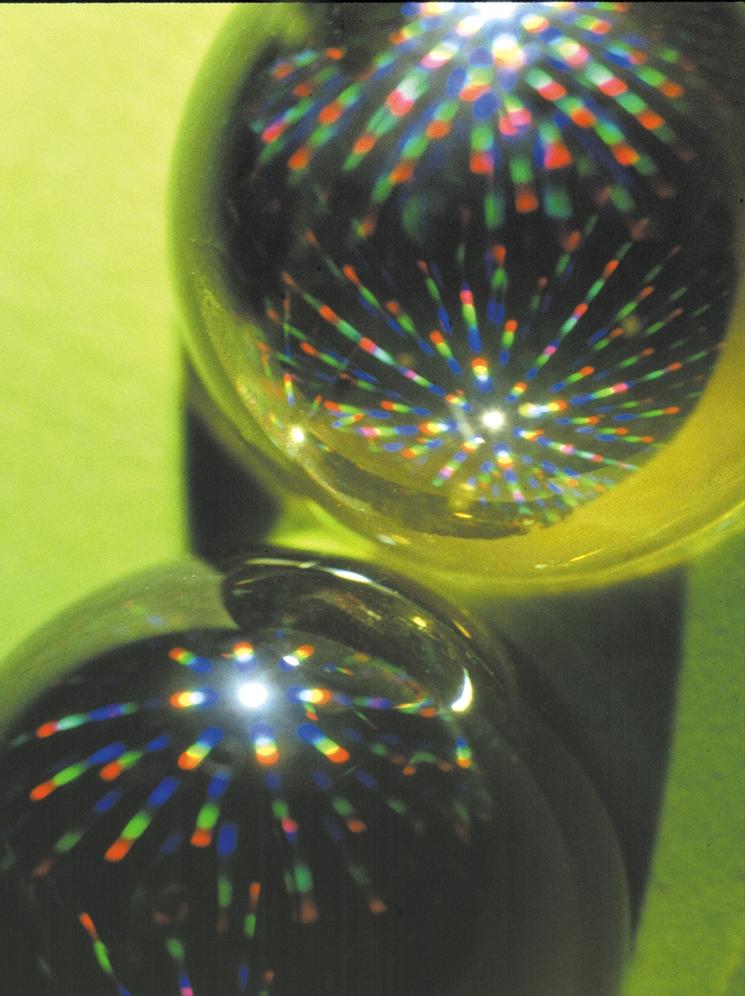
2 NANOFABRICATION art The of Building Small BY GEORGE M. WHITESIDES AND J. CHRISTOPHER LOVE RESEARCHERS ARE DISCOVERING CHEAP, EFFICIENT WAYS TO MAKE STRUCTURES ONLY A FEW BILLIONTHS OF A METER ACROSS INTRICATE DIFFRACTION PATTERNS are created by nanoscale-width rings (too small to see) on the surface of one-centimeter-wide hemispheres made of clear polymer. Kateri E. Paul, a graduate student in George M. Whitesides s group at Harvard University, fashioned the rings in a thin layer of gold on the hemispheres using a nanofabrication technique called soft lithography. SCIENTIFIC AMERICAN 39
3 Make it small! is a technological edict that has changed the world. The development of microelectronics first the transistor and then the aggregation of transistors into microprocessors, memory chips and controllers has brought forth a cornucopia of machines that manipulate information by streaming electrons through silicon. Microelectronics rests on techniques that routinely fabricate structures almost as small as 100 nanometers across (that is, 100 billionths of a meter). This size is tiny by the standards of everyday experience about one thousandth the width of a human hair but it is large on the scale of atoms and molecules. The diameter of a 100-nanometer-wide wire would span about 500 atoms of silicon. The idea of making nanostructures that comprise just one or a few atoms has great appeal, both as a scientific challenge and for practical reasons. A structure the size of an atom represents a fundamental limit: to make anything smaller would require manipulating atomic nuclei essentially, transmuting one chemical element into another. In recent years, scientists have learned various techniques for building nanostructures, but they have only just begun to Overview/Nanofabrication investigate their properties and potential applications. The age of nanofabrication is here, and the age of nanoscience has dawned, but the age of nanotechnology finding practical uses for nanostructures has not really started yet. The development of nanotechnology will depend on the ability of researchers to efficiently manufacture structures smaller than 100 nanometers (100 billionths of a meter) across. Photolithography, the technology now used to fabricate circuits on microchips, can be modified to produce nanometer-scale structures, but the modifications would be technically difficult and hugely expensive. Nanofabrication methods can be divided into two categories: top-down methods, which carve out or add aggregates of molecules to a surface, and bottom-up methods, which assemble atoms or molecules into nanostructures. Two examples of promising top-down methods are soft lithography and dip-pen lithography. Researchers are using bottom-up methods to produce quantum dots that can serve as biological dyes. The Conventional Approach RESEARCHERS may well develop nanostructures as electronic components, but the most important applications could be quite different: for example, biologists might use nanometer-scale particles as minuscule sensors to investigate cells. Because scientists do not know what kinds of nanostructures they will ultimately want to build, they have not yet determined the best ways to construct them. Photolithography, the technology used to manufacture computer chips and virtually all other microelectronic systems, can be refined to make structures smaller than 100 nanometers, but doing so is very difficult, expensive and inconvenient. In a search to find better alternatives, nanofabrication researchers have adopted the philosophy Let a thousand flowers bloom. First, consider the advantages and disadvantages of photolithography. Manufacturers use this phenomenally productive technology to churn out three billion transistors per second in the U.S. alone. Photolithography is basically an extension of photography. One first makes the equivalent of a photographic negative containing the pattern required for some part of a microchip s circuitry. This negative, which is called the mask or master, is then used to copy the pattern into the metals and semiconductors of a microchip. As is the case with photography, the negative may be hard to make, but creating multiple copies is easy, because the mask can be used many times. The process thus separates into two stages: the preparation of the mask (a one-time event, which can be slow and expensive) and the use of the mask to manufacture replicas (which must be rapid and inexpensive). To make a mask for a part of a computer chip, a manufacturer first designs the circuitry pattern on a conveniently large scale and converts it into a pattern of opaque metallic film (usually chromium) on a transparent plate (usually glass or silica). Photolithography then reduces the size of the pattern in a process analogous to that used in a photographic darkroom [see illustration on opposite page]. A beam of light (typically ultraviolet light from a mercury arc lamp) shines through the chromium mask, then passes through a lens that focuses the image onto a photosensitive coating of organic polymer (called the photoresist) on the surface of a silicon wafer. The parts of the photoresist struck by the light can be selectively removed, exposing parts of the silicon wafer in a way that replicates the original pattern. Why not use photolithography to make nanostructures? The technology faces two limitations. The first is that the shortest wavelength of ultraviolet light currently used in production processes is about 250 nanometers. Trying to make structures much smaller than half of that spacing is like trying to read print that is IMAGE BY FELICE FRANKEL, WITH TECHNICAL HELP FROM KATERI E. PAUL; COURTESY OF GEORGE M. WHITESIDES Harvard University ( page 38) 40 SCIENTIFIC AMERICAN SEPTEMBER 2001


4 BRYAN CHRISTIE too tiny: diffraction causes the features to blur and meld together. Various technical improvements have made it possible to push the limits of photolithography. The smallest structures created in mass production are somewhat larger than 100 nanometers, and complex microelectronic structures have been made with features that are only 70 nanometers across. But these structures are still not small enough to explore some of the most interesting aspects of nanoscience. The second limitation follows from the first: because it is technically difficult to make such small structures using light, it is also very expensive to do so. The photolithographic tools that will be used to make chips with features well below 100 nanometers will each cost tens to hundreds of millions of dollars. This expense may or may not be acceptable to manufacturers, but it is prohibitive for the biologists, materials scientists, chemists and physicists who wish to explore nanoscience using structures of their own design. Future Nanochips THE ELECTRONICS industry is deeply interested in developing new methods for nanofabrication so that it can continue its long-term trend of building ever smaller, faster and less expensive devices. It would be a natural evolution of microelectronics to become nanoelectronics. But because conventional photolithography becomes more difficult as the dimensions of the structures become smaller, manufacturers are exploring alternative technologies for making future nanochips. One leading contender is electronbeam lithography. In this method, the circuitry pattern is written on a thin polymer film with a beam of electrons. An electron beam does not diffract at atomic scales, so it does not cause blurring of the edges of features. Researchers have used the technique to write lines with widths of only a few nanometers in a layer of photoresist on a silicon substrate. The electron-beam instruments currently available, however, are very expensive and impractical for large-scale manufacturing. Because the beam of electrons is needed to fabricate each structure, the process is similar to the copying of a THE AUTHORS CONVENTIONAL PHOTOLITHOGRAPHY A laser beam writes the circuit pattern for a microchip on a layer of light-sensitive polymer that rests atop a layer of chromium and a glass substrate. The sections of polymer struck by the beam can be selectively removed. The exposed sections of chromium are also removed, and the rest of the polymer is dissolved. The result is a mask the equivalent of a photographic negative. When a beam of ultraviolet light is directed at the mask, the light passes through the gaps in the chromium. A lens shrinks the pattern by focusing the light onto a layer of photoresist on a silicon wafer. The exposed parts of the photoresist are removed, allowing the replication of the pattern in miniature on the silicon chips. 1 2 LASER BEAM GLASS SUBSTRATE CHROMIUM LAYER ULTRAVIOLET LIGHT manuscript by hand, one line at a time. If electrons are not the answer, what is? Another contender is lithography using x-rays with wavelengths between 0.1 and 10 nanometers or extreme ultraviolet light with wavelengths between 10 and 70 nanometers. Because these forms of radiation have much shorter wavelengths than the ultraviolet light currently used in photolithography, they minimize the blurring caused by diffraction. These technologies face their own set of problems, however: conventional lenses are not transparent to extreme ultraviolet light and do not focus x-rays. Furthermore, the energetic radiation rapidly damages many of the materials used in masks and lenses. But the microelectronics industry clearly would prefer to make advanced chips using extensions of familiar technology, so these methods are being actively developed. Some of the techniques (for example, advanced ultraviolet lithography for chip production) will probably become commercial realities. They will not, though, make inexpensive nanostructures and thus will do nothing to open nanotechnology to a broader group of scientists and engineers. The need for simpler and less expensive methods of fabricating nanostructures has stimulated the search for un- GEORGE M. WHITESIDES and J. CHRISTOPHER LOVE work together on unconventional methods of nanofabrication in the department of chemistry at Harvard University. Whitesides, a professor of chemistry, received his Ph.D. from the California Institute of Technology in 1964 and joined the Harvard faculty in Love is a graduate student and a member of Whitesides s research group. He received his bachelor s degree in chemistry from the University of Virginia in 1999 and his master s degree from Harvard in MASK 3 SILICON WAFER WITH LAYER OF PHOTORESIST SILICON CHIPS LENS SCIENTIFIC AMERICAN 41


5 SOFT LITHOGRAPHY Printing, molding and other mechanical processes carried out using an elastic stamp can produce patterns with nanoscale features. Such techniques can fabricate devices that might be used in optical communications or biochemical research. MAKING AN ELASTIC STAMP 1 A liquid precursor to polydimethylsiloxane (PDMS) is poured over a bas-relief master produced by photolithography or electron-beam lithography. 2 The liquid is cured into a rubbery solid that matches the original pattern. 3 The PDMS stamp is peeled off the master. LIQUID PRECURSOR TO PDMS PDMS STAMP MASTER PHOTORESIST MICROCONTACT PRINTING 1 The PDMS stamp is inked with a solution consisting of organic molecules called thiols and then pressed against a thin film of gold on a silicon plate. 2 The thiols form a self-assembled monolayer on the gold surface that reproduces the stamp s pattern; features in the pattern are as small as 50 nanometers. GOLD SURFACE SELF-ASSEMBLED MONOLAYER THIOL INK MICROMOLDING IN CAPILLARIES SOLIDIFIED POLYMER LIQUID POLYMER 1 The PDMS stamp is placed on a hard surface, and a liquid polymer flows into the recesses between the surface and the stamp. 2 The polymer solidifies into the desired pattern, which may contain features smaller than 10 nanometers. BRYAN CHRISTIE 42 SCIENTIFIC AMERICAN SEPTEMBER 2001
6 conventional approaches that have not been explored by the electronics industry. We first became interested in the topic in the 1990s when we were engaged in making the simple structures required in microfluidic systems chips with channels and chambers for holding liquids. This lab-on-a-chip has myriad potential uses in biochemistry, ranging from drug screening to genetic analysis. The channels in microfluidic chips are enormous by the standards of microelectronics: 50 microns (or 50,000 nanometers) wide, rather than 100 nanometers. But the techniques for producing those channels are quite versatile. Microfluidic chips can be made quickly and inexpensively, and many are composed of organic polymers and gels materials not found in the world of electronics. We discovered that matches the original pattern with astonishing fidelity: the stamp reproduces features from the master as small as a few nanometers. Although the creation of a finely detailed bas-relief master is expensive because it requires electron-beam lithography or other advanced techniques, copying the pattern on PDMS stamps is cheap and easy. And once a stamp is in hand, it can be used in various inexpensive ways to make nanostructures. The first method originally developed by Amit Kumar, a postdoctoral student in our group at Harvard University is called microcontact printing. The PDMS stamp is inked with a reagent solution consisting of organic molecules called thiols [see middle illustration on opposite page]. The stamp is then brought into contact with an appropriate sheet of These methods require no special equipment and in fact can be carried out by hand in an ordinary lab. we could use similar techniques to create nanostructures. The methods represented, in a sense, a step backward in technology. Instead of using the tools of physics light and electrons we employed mechanical processes that are familiar in everyday life: printing, stamping, molding and embossing. The techniques are called soft lithography because the tool they have in common is a block of polydimethylsiloxane (PDMS) the rubbery polymer used to caulk the leaks around bathtubs. (Physicists often refer to such organic chemicals as soft matter. ) To carry out reproduction using soft lithography, one first makes a mold or a stamp. The most prevalent procedure is to use photolithography or electronbeam lithography to produce a pattern in a layer of photoresist on the surface of a silicon wafer. This process generates a bas-relief master in which islands of photoresist stand out from the silicon [see top illustration on opposite page]. Then a chemical precursor to PDMS a freeflowing liquid is poured over the basrelief master and cured into the rubbery solid. The result is a PDMS stamp that paper a thin film of gold on a glass, silicon or polymer plate. The thiols react with the gold surface, forming a highly ordered film (called a self-assembled monolayer, or SAM) that replicates the stamp s pattern. Because the thiol ink spreads a bit after it contacts the surface, the resolution of the monolayer cannot be quite as high as that of the PDMS stamp. But when used correctly, microcontact printing can produce patterns with features as small as 50 nanometers. Another method of soft lithography, called micromolding in capillaries, involves using the PDMS stamp to mold patterns. The stamp is placed on a hard surface, and a liquid polymer flows by capillary action into the recesses between the surface and the stamp [see bottom illustration on opposite page]. The polymer then solidifies into the desired pattern. This technique can replicate structures smaller than 10 nanometers. It is particularly well suited for producing subwavelength optical devices, waveguides and optical polarizers, all of which could be used in optical fiber networks and eventually perhaps in optical computers. Other possible applications are in the field of nanofluidics, an extension of microfluidics that would involve producing chips for biochemical research with channels only a few nanometers wide. At that scale, fluid dynamics may allow new ways to separate materials such as fragments of DNA. These methods require no special equipment and in fact can be carried out by hand in an ordinary laboratory. Conventional photolithography must take place in a clean-room facility devoid of dust and dirt; if a piece of dust lands on the mask, it will create an unwanted spot on the pattern. As a result, the device being fabricated (and sometimes neighboring devices) may fail. Soft lithography is generally more forgiving because the PDMS stamp is elastic. If a piece of dust gets trapped between the stamp and the surface, the stamp will compress over the top of the particle but maintain contact with the rest of the surface. Thus, the pattern will be reproduced correctly except for where the contaminant is trapped. Moreover, soft lithography can produce nanostructures in a wide range of materials, including the complex organic molecules needed for biological studies. And the technique can print or mold patterns on curved as well as planar surfaces. But the technology is not ideal for making the structures required for complex nanoelectronics. Currently all integrated circuits consist of stacked layers of different materials. Deformations and distortions of the soft PDMS stamp can produce small errors in the replicated pattern and a misalignment of the pattern with any underlying patterns previously fabricated. Even the tiniest distortions or misalignments can destroy a multilayered nanoelectronic device. Therefore, soft lithography is not well suited for fabricating structures with multiple layers that must stack precisely on top of one another. Researchers have found ways, however, to correct this shortcoming at SCIENTIFIC AMERICAN 43

7 AFM CANTILEVER GOLD SURFACE least in part by employing a rigid stamp instead of an elastic one. In a technique called step-and-flash imprint lithography, developed by C. Grant Willson of the University of Texas, photolithography is used to etch a pattern into a quartz plate, yielding a rigid bas-relief master. Willson eliminated the step of making a PDMS stamp from the master; instead the master itself is pressed against a thin film of liquid polymer, which fills the master s recesses. Then the master is exposed to ultraviolet light, which solidifies the polymer to create the desired replica. A related technique called nanoimprint lithography, developed by Stephen Y. Chou of Princeton University, also employs a rigid master but uses a film of polymer that has been heated to a temperature near its melting point to facilitate the embossing process. Both methods can produce two-dimensional structures with good fidelity, but it remains to be seen whether the techniques are suitable for manufacturing electronic devices. Pushing Atoms Around THE CURRENT REVOLUTION in nanoscience started in 1981 with the invention of the scanning tunneling microscope (STM), for which Heinrich Rohrer and Gerd K. Binnig of the IBM Zurich DIP-PEN LITHOGRAPHY AFM TIP PYRAMIDAL TIP of an atomic force microscope (AFM) is coated with a thin film of thiol molecules. A minute drop of water condenses between the microscope s tip and a gold surface. The thiols migrate from the tip to the surface, where they form a self-assembled monolayer. THIOL MOLECULES DROP OF WATER SELF-ASSEMBLED MONOLAYER Research Laboratory received the Nobel Prize in Physics in This remarkable device detects small currents that pass between the microscope s tip and the sample being observed, allowing researchers to see substances at the scale of individual atoms. The success of the STM led to the development of other scanning probe devices, including the atomic force microscope (AFM). The operating principle of the AFM is similar to that of an old-fashioned phonograph. A tiny probe a fiber or a pyramid-shaped tip that is typically between two and 30 nanometers wide is brought into direct contact with the sample. The probe is attached to the end of a cantilever, which bends as the tip moves across the sample s surface. The deflection is measured by reflecting a beam of laser light off the top of the cantilever. The AFM can detect variations in vertical surface topography that are smaller than the dimensions of the probe. But scanning probe devices can do more than simply allow scientists to observe the atomic world they can also be used to create nanostructures. The tip on the AFM can be used to physically move nanoparticles around on surfaces and to arrange them in patterns. It can also be used to make scratches in a surface (or more commonly, in monolayer films of atoms or molecules that coat the surface). Similarly, if researchers increase the currents flowing from the tip of the STM, the microscope becomes a very small source for an electron beam, which can be used to write nanometer-scale patterns. The STM tip can also push individual atoms around on a surface to build rings and wires that are only one atom wide. An intriguing new scanning probe fabrication method is called dip-pen lithography. Developed by Chad A. Mirkin of Northwestern University, this technique works much like a goose-feather pen [see illustration at left]. The tip of the AFM is coated with a thin film of thiol molecules that are insoluble in water but react with a gold surface (the same chemistry used in microcontact printing). When the device is placed in an atmosphere containing a high concentration of water vapor, a minute drop of water condenses between the gold surface and the microscope s tip. Surface tension pulls the tip to a fixed distance from the gold, and this distance does not change as the tip moves across the surface. The drop of water acts as a bridge over which the thiol molecules migrate from the tip to the gold surface, where they are fixed. Researchers have used this procedure to write lines a few nanometers across. Although dip-pen lithography is relatively slow, it can use many different types of molecules as inks and thus brings great chemical flexibility to nanometer-scale writing. Researchers have not yet determined the best applications for the technique, but one idea is to use the dip-pen method for precise modifications of circuit designs. Mirkin has recently demonstrated that a variant of the ink used in dip-pen lithography can write directly on silicon. An interesting cousin to these techniques involves another kind of nanostructure, called a break junction. If you break a thin, ductile metal wire into two parts by pulling sharply, the process seems abrupt to a human observer, but it actually follows a complex sequence. When the force used in breaking the wire is first applied, the metal begins to yield and flow, and the diameter of the wire BRYAN CHRISTIE 44 SCIENTIFIC AMERICAN SEPTEMBER 2001
8 decreases. As the two ends move apart, the wire gets thinner and thinner until, in the instant just before breaking, it is a single atom in diameter at its narrowest point. This process of thinning a wire to a break junction can be detected easily by measuring the current that flows through the wire. When the wire is slender enough, current can flow only in discrete quantities (that is, current flow is quantized). The break junction is analogous to two STM tips facing each other, and similar physical rules govern the current that flows through it. Mark A. Reed of Yale University has pioneered a particularly inventive use of the break junction. He built a device that enabled a thin junction to be broken under carefully controlled conditions and then allowed the broken tips to be brought back together or to be held apart at any distance with an accuracy of a few thousandths of a nanometer. By adjusting the distance between the tips in the presence of an organic molecule that bridged them, Reed was able to measure a current flowing across the organic bridge. This experiment was an important step in the development of technologies for using single organic molecules as electronic devices such as diodes and transistors [see Computing with Molecules, by Mark A. Reed and James M. Tour; Scientific American, June 2000]. Top-Down and Bottom-Up ALL THE FORMS of lithography we have discussed so far are called top-down methods that is, they begin with a pattern generated on a larger scale and reduce its lateral dimensions (often by a factor of 10) before carving out nanostructures. This strategy is required in fabricating electronic devices such as microchips, whose functions depend more on their patterns than on their dimensions. But no top-down method is ideal; none can conveniently, cheaply and quickly make nanostructures of any material. So researchers have shown growing interest in bottom-up methods, which start with atoms or molecules and build up to nanostructures. These methods can easily make the smallest nanostructures with dimensions between two and 10 nanometers and do so inexpensively. But these structures are usually generated as simple particles in suspension or on surfaces, rather than as designed, interconnected patterns. Two of the most prominent bottomup methods are those used to make nanotubes and quantum dots. Scientists have made long, cylindrical tubes of carbon by a catalytic growth process that employs a nanometer-scale drop of molten metal (usually iron) as a catalyst [see Nanotubes for Electronics, by Philip G. Collins and Phaedon Avouris; Scientific American, December 2000]. The most active area of research in quantum dots originated in the laboratory of Louis E. Brus (then at Bell Laboratories) and has been developed by A. Paul Alivisatos of the University of California at Berkeley, Moungi G. Bawendi of the Massachusetts Institute of Technology, and others. Quantum dots are crystals containing only a few hundred atoms. Because the electrons in a quantum dot are confined to widely separated energy levels, the dot emits only one wavelength of light when it is excited. This property makes the quantum dot useful as a biological marker [see Nanofabrication: Comparing the Methods Researchers are developing an array of techniques for building structures smaller than 100 nanometers. Here is a summary of the advantages and disadvantages of four methods. Photolithography Advantages: The electronics industry is already familiar with this technology because it is currently used to fabricate microchips. Manufacturers can modify the technique to produce nanometer-scale structures by employing electron beams, x-rays or extreme ultraviolet light. Disadvantages: The necessary modifications will be expensive and technically difficult. Using electron beams to fashion structures is costly and slow. X-rays and extreme ultraviolet light can damage the equipment used in the process. Soft Lithography Advantages: This method allows researchers to inexpensively reproduce patterns created by electron-beam lithography or other related techniques. Soft lithography requires no special equipment and can be carried out by hand in an ordinary laboratory. Disadvantages: The technique is not ideal for manufacturing the multilayered structures of electronic devices. Researchers are trying to overcome this drawback, but it remains to be seen whether these efforts will be successful. Scanning Probe Methods Advantages: The scanning tunneling microscope and the atomic force microscope can be used to move individual nanoparticles and arrange them in patterns. The instruments can build rings and wires that are only one atom wide. Disadvantages: The methods are too slow for mass production. Applications of the microscopes will probably be limited to the fabrication of specialized devices. Bottom-Up Methods Advantages: By setting up carefully controlled chemical reactions, researchers can cheaply and easily assemble atoms and molecules into the smallest nanostructures, with dimensions between two and 10 nanometers. Disadvantages: Because these methods cannot produce designed, interconnected patterns, they are not well suited for building electronic devices such as microchips. SCIENTIFIC AMERICAN 45


![When the crystal reaches its optimum size, the organic molecules coat its surface in a stable packing. Less Is More in Medicine, on page 66].](/docs-images/94/120821661/images/9-2.jpg "One procedure used to make quantum dots involves a chemical reaction between a metal ion (for example, cadmium) and a molecule that is able to donate a selenium ion.")
9 QUANTUM DOT ASSEMBLY Crystals called quantum dots contain only a few hundred atoms and emit different wavelengths of light, depending on their size. They may become useful as biological markers of cellular activity A chemical reaction brings together cadmium ions (purple), selenium ions (green) and organic molecules (red spheres with blue tails). The organic molecules act as surfactants, binding to the surface of the cadmium selenide crystal as it grows. When the crystal reaches its optimum size, the organic molecules coat its surface in a stable packing. Less Is More in Medicine, on page 66]. One procedure used to make quantum dots involves a chemical reaction between a metal ion (for example, cadmium) and a molecule that is able to donate a selenium ion. This reaction generates crystals of cadmium selenide. The trick is to prevent the small crystals from sticking together as they grow to the desired size. To insulate the growing particles from one another, researchers carry out the reaction in the presence of organic molecules that act as surfactants, coating the surface of each cadmium selenide particle as it grows. The organic molecules stop the crystals from clumping together and regulate their rate of growth. The geometry of the particles can be controlled to some extent by mixing different ratios of the organic molecules. The reaction can generate particles with a variety of shapes, including spheres, rods and tetrapods (four-armed particles similar to toy jacks). It is important to synthesize the quantum dots with uniform size and composition, because the size of the dot determines its electronic, magnetic and optical properties. Researchers can select the size of the particles by varying the length of time for the reaction. The organic coating also helps to set the size of the particles. When the nanoparticle is small (on the scale of molecules), the organic coating is loose and allows further growth; as the particle enlarges, the organic molecules become crowded. There is an optimum size for the particles that allows the most stable packing of the organic molecules and thus provides the greatest stabilization for the surfaces of the crystals. These cadmium selenide nanoparticles promise some of the first commercial products of nanoscience: Quantum Dot Corporation has been developing the crystals for use as biological labels. Researchers can tag proteins and nucleic acids with quantum dots; when the sample is illuminated with ultraviolet light, the crystals will fluoresce at a specific wavelength and thus show the locations of the attached proteins. Many organic molecules also fluoresce, but quantum dots have several advantages that make them better markers. First, the color of BRYAN CHRISTIE 46 SCIENTIFIC AMERICAN SEPTEMBER 2001
10 a quantum dot s fluorescence can be tailored by changing the dot s size: the larger the particle, the more the emitted light is shifted toward the red end of the spectrum. Second, if all the dots are the same size, their fluorescence spectrum is narrow that is, they emit a very pure color. This property is important because it allows particles of different sizes to be used as distinguishable labels. Third, the fluorescence of quantum dots does not fade on exposure to ultraviolet light, as does that of organic molecules. When used as dyes in biological research, the dots can be observed for conveniently long periods. Scientists are also investigating the possibility of making structures from colloids nanoparticles in suspension. Christopher B. Murray and a team at the IBM Thomas J. Watson Research Center are exploring the use of such colloids to create a medium for ultrahigh-density data storage. The IBM team s colloids contain magnetic nanoparticles as small as mammalian cells are larger. Cells are, however, filled with much smaller structures, many of which are astonishingly sophisticated. The ribosome, for example, carries out one of the most important cellular functions: the synthesis of proteins from amino acids, using messenger RNA as the template. The complexity of this molecular construction project far surpasses that of man-made techniques. Or consider the rotary motors of the bacterial flagella, which efficiently propel the one-celled organisms [see The Once and Future Nanomachine, on page 78]. It is unclear if nanomachines taken from cells will be useful. They will probably have very limited application in electronics, but they may provide valuable tools for chemical synthesis and sensing devices. Recent work by Carlo D. Montemagno of Cornell University has shown that it is possible to engineer a primitive nanomachine with a biological engine. Montemagno extracted a rotary motor protein from a bacterial cell and The development of nanotechnology will depend on the availability of nanostructures. The invention of the STM and AFM has provided new tools for viewing, characterizing and manipulating these structures; the issue now is how to build them to order and how to design them to have new and useful functions. The importance of electronics applications has tended to focus attention on nanodevices that might be incorporated into future integrated circuits. And for good technological reasons, the electronics industry has emphasized fabrication methods that are extensions of those currently used to make microchips. But the explosion of interest in nanoscience has created a demand for a broad range of fabrication methods, with an emphasis on low-cost, convenient techniques. The new approaches to nanofabrication are unconventional only because they are not derived from the microtechnology developed for electronic devices. Bottom-up methods start from atoms or molecules and build up to nanostructures. three nanometers across, each composed of about 1,000 iron and platinum atoms. When the colloid is spread on a surface and the solvent allowed to evaporate, the nanoparticles crystallize in two- or three-dimensional arrays. Initial studies indicate that these arrays can potentially store trillions of bits of data per square inch, giving them a capacity 10 to 100 times greater than that of present memory devices. The Future of Nanofabrication THE INTEREST in nanostructures is so great that every plausible fabrication technique is being examined. Although physicists and chemists are now doing most of the work, biologists may also make important contributions. The cell (whether mammalian or bacterial) is relatively large on the scale of nanostructures: the typical bacterium is approximately 1,000 nanometers long, and connected it to a metallic nanorod a cylinder 750 nanometers long and 150 nanometers wide that had been fabricated by lithography. The rotary motor, which was only 11 nanometers tall, was powered by adenosine triphosphate (ATP), the source of chemical energy in cells. Montemagno showed that the motor could rotate the nanorod at eight revolutions per minute. At the very least, such research stimulates efforts to fabricate functional nanostructures by demonstrating that such structures can exist. MORE TO EXPLORE Chemists, physicists and biologists are rapidly accepting these techniques as the most appropriate ways to build various kinds of nanostructures for research. And the methods may even supplement the conventional approaches photolithography, electron-beam lithography and related techniques for applications in electronics as well. The microelectronics mold is now broken. Ideas for nanofabrication are coming from many directions in a wonderful free-for-all of discovery. More information about nanofabrication can be found at the following Web sites: International SEMATECH: The Whitesides group at Harvard University: gmwgroup.harvard.edu The Mirkin group at Northwestern University: The Willson group at the University of Texas at Austin: willson.cm.utexas.edu/research/research.htm The Alivisatos group at the University of California at Berkeley: The Bawendi group at M.I.T.: web.mit.edu/chemistry/nanocluster/ The Montemagno group at Cornell University: falcon.aben.cornell.edu/ SCIENTIFIC AMERICAN 47
Nanotechnology Fabrication Methods.
 Nanotechnology Fabrication Methods. 10 / 05 / 2016 1 Summary: 1.Introduction to Nanotechnology:...3 2.Nanotechnology Fabrication Methods:...5 2.1.Top-down Methods:...7 2.2.Bottom-up Methods:...16 3.Conclusions:...19
Kavli Workshop for Journalists. June 13th, CNF Cleanroom Activities
 Kavli Workshop for Journalists June 13th, 2007 CNF Cleanroom Activities Seeing nm-sized Objects with an SEM Lab experience: Scanning Electron Microscopy Equipment: Zeiss Supra 55VP Scanning electron microscopes
Final Reading Assignment: Travels to the Nanoworld: pages pages pages
 Final Reading Assignment: Travels to the Nanoworld: pages 152-164 pages 201-214 pages 219-227 Bottom-up nanofabrication Can we assemble nanomachines manually? What are the components (parts)? nanoparticles
Introduction to Photolithography
 http://www.ichaus.de/news/72 Introduction to Photolithography Photolithography The following slides present an outline of the process by which integrated circuits are made, of which photolithography is
Chapter 10. Nanometrology. Oxford University Press All rights reserved.
 Chapter 10 Nanometrology Oxford University Press 2013. All rights reserved. 1 Introduction Nanometrology is the science of measurement at the nanoscale level. Figure illustrates where nanoscale stands
Nanotechnology Nanofabrication of Functional Materials. Marin Alexe Max Planck Institute of Microstructure Physics, Halle - Germany
 Nanotechnology Nanofabrication of Functional Materials Marin Alexe Max Planck Institute of Microstructure Physics, Halle - Germany Contents Part I History and background to nanotechnology Nanoworld Nanoelectronics
NANOTECHNOLOGY. Students will gain an understanding of nanoscale dimensions and nanotechnology.
 NANOTECHNOLOGY By Anna M. Waldron and Carl A. Batt, Nanobiotechnology Center, Cornell University Subjects: Nanotechnology, Chemistry, Physics Time: Two class periods (approximately 90 minutes) Objective:
Unconventional Nano-patterning. Peilin Chen
 Unconventional Nano-patterning Peilin Chen Reference Outlines History of patterning Traditional Nano-patterning Unconventional Nano-patterning Ancient Patterning "This is the Elks' land". A greeting at
Nanostructures Fabrication Methods
 Nanostructures Fabrication Methods bottom-up methods ( atom by atom ) In the bottom-up approach, atoms, molecules and even nanoparticles themselves can be used as the building blocks for the creation of
Figure 1: Some examples of objects at different size scales ( 2001, CMP Científica, [2])
![Figure 1: Some examples of objects at different size scales ( 2001, CMP Científica, [2])](/thumbs/85/91872790.jpg "Figure 1: Some examples of objects at different size scales ( 2001, CMP Científica, [2])") Top-Down vs. Bottom-Up Nanomanufacturing Prof. Derek J. Hansford, Biomedical Engineering Program and Department of Materials Science & Engineering Learning Objectives: This module should expose the student
Top-Down vs. Bottom-Up Nanomanufacturing Prof. Derek J. Hansford, Biomedical Engineering Program and Department of Materials Science & Engineering Learning Objectives: This module should expose the student
Lesson 4: Tools of the Nanosciences. Student Materials
 Lesson 4: Tools of the Nanosciences Student Materials Contents Black Box Lab Activity: Student Instructions and Worksheet Seeing and Building Small Things: Student Reading Seeing and Building Small Things:
Far IR Gas Lasers microns wavelengths, THz frequency Called Terahertz lasers or FIR lasers At this wavelength behaves more like
 Far IR Gas Lasers 10-1500 microns wavelengths, 300 10 THz frequency Called Terahertz lasers or FIR lasers At this wavelength behaves more like microwave signal than light Created by Molecular vibronic
Fabrication at the nanoscale for nanophotonics
 Fabrication at the nanoscale for nanophotonics Ilya Sychugov, KTH Materials Physics, Kista silicon nanocrystal by electron beam induced deposition lithography Outline of basic nanofabrication methods Devices
In the name of Allah
 In the name of Allah Nano chemistry- 4 th stage Lecture No. 1 History of nanotechnology 16-10-2016 Assistance prof. Dr. Luma Majeed Ahmed lumamajeed2013@gmail.com, luma.ahmed@uokerbala.edu.iq Nano chemistry-4
Nanomaterials and their Optical Applications
 Nanomaterials and their Optical Applications Winter Semester 2013 Lecture 02 rachel.grange@uni-jena.de http://www.iap.uni-jena.de/multiphoton Lecture 2: outline 2 Introduction to Nanophotonics Theoretical
0 volts. 2 volts. 5 volts
 CS101 Binary Storage Devices and Boolean Logic Now that we have discussed number representation, why do computers use the binary representation and not something we are more familiar with, like decimal?
National Science and Technology Council (NSTC) Committee on Technology
 Committee on Technology") BY LYNN YARRIS "The emerging fields of nanoscience and nanoengineering are leading to unprecedented understanding and control over the fundamental building blocks of all physical things. This is likely
BY LYNN YARRIS "The emerging fields of nanoscience and nanoengineering are leading to unprecedented understanding and control over the fundamental building blocks of all physical things. This is likely
Nanotechnology. Gavin Lawes Department of Physics and Astronomy
 Nanotechnology Gavin Lawes Department of Physics and Astronomy Earth-Moon distance 4x10 8 m (courtesy NASA) Length scales (Part I) Person 2m Magnetic nanoparticle 5x10⁻⁹ m 10 10 m 10 5 m 1 m 10-5 m 10-10
MRSEC. Refrigerator Magnet Activity Guide. Quick Reference Activity Guide. a) b) c) = north = south. Activity Materials
 b) c) = north = south. Activity Materials") MRSEC Refrigerator Magnet Activity Guide Quick Reference Activity Guide Activity Materials Refrigerator magnet with removable probe strip Magnetic field diagrams Starting Points One of the great breakthroughs
MRSEC Refrigerator Magnet Activity Guide Quick Reference Activity Guide Activity Materials Refrigerator magnet with removable probe strip Magnetic field diagrams Starting Points One of the great breakthroughs
From nanophysics research labs to cell phones. Dr. András Halbritter Department of Physics associate professor
 From nanophysics research labs to cell phones Dr. András Halbritter Department of Physics associate professor Curriculum Vitae Birth: 1976. High-school graduation: 1994. Master degree: 1999. PhD: 2003.
Nanostructures. Lecture 13 OUTLINE
 Nanostructures MTX9100 Nanomaterials Lecture 13 OUTLINE -What is quantum confinement? - How can zero-dimensional materials be used? -What are one dimensional structures? -Why does graphene attract so much
Chapter 12 - Modern Materials
 Chapter 12 - Modern Materials 12.1 Semiconductors Inorganic compounds that semiconduct tend to have chemical formulas related to Si and Ge valence electron count of four. Semiconductor conductivity can
General concept and defining characteristics of AFM. Dina Kudasheva Advisor: Prof. Mary K. Cowman
 General concept and defining characteristics of AFM Dina Kudasheva Advisor: Prof. Mary K. Cowman Overview Introduction History of the SPM invention Technical Capabilities Principles of operation Examples
Nanotechnology. Yung Liou P601 Institute of Physics Academia Sinica
 Nanotechnology Yung Liou P601 yung@phys.sinica.edu.tw Institute of Physics Academia Sinica 1 1st week Definition of Nanotechnology The Interagency Subcommittee on Nanoscale Science, Engineering and Technology
CURRENT STATUS OF NANOIMPRINT LITHOGRAPHY DEVELOPMENT IN CNMM
 U.S. -KOREA Forums on Nanotechnology 1 CURRENT STATUS OF NANOIMPRINT LITHOGRAPHY DEVELOPMENT IN CNMM February 17 th 2005 Eung-Sug Lee,Jun-Ho Jeong Korea Institute of Machinery & Materials U.S. -KOREA Forums
There s plenty of room at the bottom! - R.P. Feynman, Nanostructure: a piece of material with at least one dimension less than 100 nm in extent.
 Nanostructures and Nanotechnology There s plenty of room at the bottom! - R.P. Feynman, 1959 Materials behave differently when structured at the nm scale than they do in bulk. Technologies now exist that
Introduction to Scanning Probe Microscopy
 WORKSHOP Nanoscience on the Tip Introduction to Scanning Probe Microscopy Table of Contents: 1 Historic Perspectives... 1 2 Scanning Force Microscopy (SFM)... 2 2.1. Contact Mode... 2 2.2. AC Mode Imaging...
Nanotechnology where size matters
 Nanotechnology where size matters J Emyr Macdonald Overview Ways of seeing very small things What is nanotechnology and why is it important? Building nanostructures What we can do with nanotechnology?
Far IR (FIR) Gas Lasers microns wavelengths, THz frequency Called Terahertz lasers or FIR lasers At this wavelength behaves more like
 Gas Lasers microns wavelengths, THz frequency Called Terahertz lasers or FIR lasers At this wavelength behaves more like") Far IR (FIR) Gas Lasers 10-1500 microns wavelengths, 300 10 THz frequency Called Terahertz lasers or FIR lasers At this wavelength behaves more like microwave signal than light Created by Molecular vibronic
Far IR (FIR) Gas Lasers 10-1500 microns wavelengths, 300 10 THz frequency Called Terahertz lasers or FIR lasers At this wavelength behaves more like microwave signal than light Created by Molecular vibronic
Subject Index. See https://pubs.acs.org/sharingguidelines for options on how to legitimately share published articles.
 Subject Index Downloaded via 148.251.232.83 on July 22, 2018 at 01:11:58 (UTC). See https://pubs.acs.org/sharingguidelines for options on how to legitimately share published articles. A American Chemical
1.1. Introduction to Nanoscience and Nanotechnology
 1.1. Introduction to Nanoscience and Nanotechnology 1.1.1. A Brief Historical Overview Before trying to understand and discuss about synthesis, characterization and application of nanomaterials, it is
Nanoscale Issues in Materials & Manufacturing
 Nanoscale Issues in Materials & Manufacturing ENGR 213 Principles of Materials Engineering Module 2: Introduction to Nanoscale Issues Top-down and Bottom-up Approaches for Fabrication Winfried Teizer,
Nanotechnology? Source: National Science Foundation (NSF), USA
, USA") 2 2 Nanotechnology? Ability to work at the atomic, molecular and even sub-molecular levels in order to create and use material structures, devices and systems with new properties and functions Source:
2 2 Nanotechnology? Ability to work at the atomic, molecular and even sub-molecular levels in order to create and use material structures, devices and systems with new properties and functions Source:
CHAPTER 11 Semiconductor Theory and Devices
 CHAPTER 11 Semiconductor Theory and Devices 11.1 Band Theory of Solids 11.2 Semiconductor Theory 11.3 Semiconductor Devices 11.4 Nanotechnology It is evident that many years of research by a great many
Scanning Probe Microscopy. Amanda MacMillan, Emmy Gebremichael, & John Shamblin Chem 243: Instrumental Analysis Dr. Robert Corn March 10, 2010
 Scanning Probe Microscopy Amanda MacMillan, Emmy Gebremichael, & John Shamblin Chem 243: Instrumental Analysis Dr. Robert Corn March 10, 2010 Scanning Probe Microscopy High-Resolution Surface Analysis
Communicating Research to the General Public
 Communicating Research to the General Public At the March 5, 2010 UW-Madison Chemistry Department Colloquium, the director of the Wisconsin Initiative for Science Literacy (WISL) encouraged all Ph.D. chemistry
Computers of the Future? Moore s Law Ending in 2018?
 Computers of the Future? CS 221 Moore s Law Ending in 2018? Moore s Law: Processor speed / number transistors doubling approximately 18 months 1 Moore s Law Moore s Law Recent research predicts an end
MEEN Nanoscale Issues in Manufacturing. Lithography Lecture 1: The Lithographic Process
 MEEN 489-500 Nanoscale Issues in Manufacturing Lithography Lecture 1: The Lithographic Process 1 Discuss Reading Assignment 1 1 Introducing Nano 2 2 Size Matters 3 3 Interlude One-The Fundamental Science
Nanosphere Lithography
 Nanosphere Lithography Derec Ciafre 1, Lingyun Miao 2, and Keita Oka 1 1 Institute of Optics / 2 ECE Dept. University of Rochester Abstract Nanosphere Lithography is quickly emerging as an efficient, low
I. NANOFABRICATION O AND CHARACTERIZATION Chap. 2 : Self-Assembly
 I. Nanofabrication and Characterization : TOC I. NANOFABRICATION O AND CHARACTERIZATION Chap. 1 : Nanolithography Chap. 2 : Self-Assembly Chap. 3 : Scanning Probe Microscopy Nanoscale fabrication requirements
Scanning Tunneling Microscopy
 Scanning Tunneling Microscopy References: 1. G. Binnig, H. Rohrer, C. Gerber, and Weibel, Phys. Rev. Lett. 49, 57 (1982); and ibid 50, 120 (1983). 2. J. Chen, Introduction to Scanning Tunneling Microscopy,
CORE MOLIT ACTIVITIES at a glance
 CORE MOLIT ACTIVITIES at a glance 1. Amplification of Biochemical Signals: The ELISA Test http://molit.concord.org/database/activities/248.html The shape of molecules affects the way they function. A test
Nano-mechatronics. Presented by: György BudaváriSzabó (X0LY4M)
") Nano-mechatronics Presented by: György BudaváriSzabó (X0LY4M) Nano-mechatronics Nano-mechatronics is currently used in broader spectra, ranging from basic applications in robotics, actuators, sensors,
Nano-mechatronics Presented by: György BudaváriSzabó (X0LY4M) Nano-mechatronics Nano-mechatronics is currently used in broader spectra, ranging from basic applications in robotics, actuators, sensors,
Overview of the main nano-lithography techniques
 Overview of the main nano-lithography techniques Soraya Sangiao sangiao@unizar.es Outline Introduction: Nanotechnology. Nano-lithography techniques: Masked lithography techniques: Photolithography. X-ray
CHARACTERIZATION of NANOMATERIALS KHP
 CHARACTERIZATION of NANOMATERIALS Overview of the most common nanocharacterization techniques MAIN CHARACTERIZATION TECHNIQUES: 1.Transmission Electron Microscope (TEM) 2. Scanning Electron Microscope
ESH Benign Processes for he Integration of Quantum Dots (QDs)
") ESH Benign Processes for he Integration of Quantum Dots (QDs) PIs: Karen K. Gleason, Department of Chemical Engineering, MIT Graduate Students: Chia-Hua Lee: PhD Candidate, Department of Material Science
ESH Benign Processes for he Integration of Quantum Dots (QDs) PIs: Karen K. Gleason, Department of Chemical Engineering, MIT Graduate Students: Chia-Hua Lee: PhD Candidate, Department of Material Science
Imaging Methods: Scanning Force Microscopy (SFM / AFM)
") Imaging Methods: Scanning Force Microscopy (SFM / AFM) The atomic force microscope (AFM) probes the surface of a sample with a sharp tip, a couple of microns long and often less than 100 Å in diameter.
Imaging Methods: Scanning Force Microscopy (SFM / AFM) The atomic force microscope (AFM) probes the surface of a sample with a sharp tip, a couple of microns long and often less than 100 Å in diameter.
29: Nanotechnology. What is Nanotechnology? Properties Control and Understanding. Nanomaterials
 29: Nanotechnology What is Nanotechnology? Properties Control and Understanding Nanomaterials Making nanomaterials Seeing at the nanoscale Quantum Dots Carbon Nanotubes Biology at the Nanoscale Some Applications
Investigating Nano-Space
 Name Partners Date Visual Quantum Mechanics The Next Generation Investigating Nano-Space Goal You will apply your knowledge of tunneling to understand the operation of the scanning tunneling microscope.
There's Plenty of Room at the Bottom
 There's Plenty of Room at the Bottom 12/29/1959 Feynman asked why not put the entire Encyclopedia Britannica (24 volumes) on a pin head (requires atomic scale recording). He proposed to use electron microscope
Inorganic compounds that semiconduct tend to have an average of 4 valence electrons, and their conductivity may be increased by doping.
 Chapter 12 Modern Materials 12.1 Semiconductors Inorganic compounds that semiconduct tend to have an average of 4 valence electrons, and their conductivity may be increased by doping. Doping yields different
Photolithography 光刻 Part II: Photoresists
 微纳光电子材料与器件工艺原理 Photolithography 光刻 Part II: Photoresists Xing Sheng 盛兴 Department of Electronic Engineering Tsinghua University xingsheng@tsinghua.edu.cn 1 Photolithography 光刻胶 负胶 正胶 4 Photolithography
RAJASTHAN TECHNICAL UNIVERSITY, KOTA
 RAJASTHAN TECHNICAL UNIVERSITY, KOTA (Electronics & Communication) Submitted By: LAKSHIKA SOMANI E&C II yr, IV sem. Session: 2007-08 Department of Electronics & Communication Geetanjali Institute of Technical
Understanding the properties and behavior of groups of interacting atoms more than simple molecules
 Condensed Matter Physics Scratching the Surface Understanding the properties and behavior of groups of interacting atoms more than simple molecules Solids and fluids in ordinary and exotic states low energy
Quantum Dots: Applications in Modern. Technology
 Quantum Dots 1 Quantum Dots: Applications in Modern Technology K. Li and R. Lan Optical Engineering Dr. K. Daneshvar July 13, 2007 Quantum Dots 2 Abstract: As technology moves forward, the need for semiconductors
Nanophysics: Main trends
 Nano-opto-electronics Nanophysics: Main trends Nanomechanics Main issues Light interaction with small structures Molecules Nanoparticles (semiconductor and metallic) Microparticles Photonic crystals Nanoplasmonics
Dip-Pen Lithography 1
 Dip-Pen Lithography 1 A Brief History of Writing Instruments From Quills and Bamboos to fountain pens and brushes M. Klein and Henry W. Wynne received US patent #68445 in 1867 for an ink chamber and delivery
NANOSCIENCE: TECHNOLOGY AND ADVANCED MATERIALS
 UNIVERSITY OF SOUTHAMPTON PHYS6014W1 SEMESTER 2 EXAMINATIONS 2012-2013 NANOSCIENCE: TECHNOLOGY AND ADVANCED MATERIALS DURATION 120 MINS (2 Hours) This paper contains 8 questions Answer ALL questions in
Techniken der Oberflächenphysik (Techniques of Surface Physics)
") Techniken der Oberflächenphysik (Techniques of Surface Physics) Prof. Yong Lei & Dr. Yang Xu Fachgebiet 3D-Nanostrukturierung, Institut für Physik Contact: yong.lei@tu-ilmenau.de yang.xu@tu-ilmenau.de
Techniken der Oberflächenphysik (Techniques of Surface Physics) Prof. Yong Lei & Dr. Yang Xu Fachgebiet 3D-Nanostrukturierung, Institut für Physik Contact: yong.lei@tu-ilmenau.de yang.xu@tu-ilmenau.de
Far IR (FIR) Gas Lasers microns wavelengths, THz frequency Called Terahertz lasers or FIR lasers At this wavelength behaves more like
 Gas Lasers microns wavelengths, THz frequency Called Terahertz lasers or FIR lasers At this wavelength behaves more like") Far IR (FIR) Gas Lasers 10-1500 microns wavelengths, 300 10 THz frequency Called Terahertz lasers or FIR lasers At this wavelength behaves more like microwave signal than light Created by Molecular vibronic
Far IR (FIR) Gas Lasers 10-1500 microns wavelengths, 300 10 THz frequency Called Terahertz lasers or FIR lasers At this wavelength behaves more like microwave signal than light Created by Molecular vibronic
How To Grow a Super Material or Troubleshoot a Classic One
 How To Grow a Super Material or Troubleshoot a Classic One David A. Muller APPLIED AND ENGINEERING PHYSICS Being able to see each atom of a material has allowed us to troubleshoot, discover, and create
MSN551 LITHOGRAPHY II
 MSN551 Introduction to Micro and Nano Fabrication LITHOGRAPHY II E-Beam, Focused Ion Beam and Soft Lithography Why need electron beam lithography? Smaller features are required By electronics industry:
MATERIAL SCIENCE AND TECHONOLOGY-1. Scanning Tunneling Microscope, STM Tunneling Electron Microscope, TEM HATİCE DOĞRUOĞLU
 MATERIAL SCIENCE AND TECHONOLOGY-1 Scanning Tunneling Microscope, STM Tunneling Electron Microscope, TEM HATİCE DOĞRUOĞLU Scanning Tunelling Microscope (STM) In 1981,Gerd Binnig and Heinrich Rohrer and
The Intersection of Chemistry and Biology: An Interview with Professor W. E. Moerner
 The Intersection of Chemistry and Biology: An Interview with Professor W. E. Moerner Joseph Nicolls Stanford University Professor W.E Moerner earned two B.S. degrees, in Physics and Electrical Engineering,
Chapter 12. Nanometrology. Oxford University Press All rights reserved.
 Chapter 12 Nanometrology Introduction Nanometrology is the science of measurement at the nanoscale level. Figure illustrates where nanoscale stands in relation to a meter and sub divisions of meter. Nanometrology
Scripts for High School Visits to the Herman Group at Columbia University
 Scripts for High School Visits to the Herman Group at Columbia University Evan Spotte-Smith, Jiayang Hu, and Irving P. Herman April, 2017; updated June, 2017 These presentations were developed for visits
CSCI 2570 Introduction to Nanocomputing
 CSCI 2570 Introduction to Nanocomputing The Emergence of Nanotechnology John E Savage Purpose of the Course The end of Moore s Law is in sight. Researchers are now exploring replacements for standard methods
UNIT 3. By: Ajay Kumar Gautam Asst. Prof. Dev Bhoomi Institute of Technology & Engineering, Dehradun
 UNIT 3 By: Ajay Kumar Gautam Asst. Prof. Dev Bhoomi Institute of Technology & Engineering, Dehradun 1 Syllabus Lithography: photolithography and pattern transfer, Optical and non optical lithography, electron,
Seminars in Nanosystems - I
 Seminars in Nanosystems - I Winter Semester 2011/2012 Dr. Emanuela Margapoti Emanuela.Margapoti@wsi.tum.de Dr. Gregor Koblmüller Gregor.Koblmueller@wsi.tum.de Seminar Room at ZNN 1 floor Topics of the
Nanobiotechnology. Place: IOP 1 st Meeting Room Time: 9:30-12:00. Reference: Review Papers. Grade: 40% midterm, 60% final report (oral + written)
") Nanobiotechnology Place: IOP 1 st Meeting Room Time: 9:30-12:00 Reference: Review Papers Grade: 40% midterm, 60% final report (oral + written) Midterm: 5/18 Oral Presentation 1. 20 minutes each person
Nanobiotechnology Place: IOP 1 st Meeting Room Time: 9:30-12:00 Reference: Review Papers Grade: 40% midterm, 60% final report (oral + written) Midterm: 5/18 Oral Presentation 1. 20 minutes each person
Fabrication and Domain Imaging of Iron Magnetic Nanowire Arrays
 Abstract #: 983 Program # MI+NS+TuA9 Fabrication and Domain Imaging of Iron Magnetic Nanowire Arrays D. A. Tulchinsky, M. H. Kelley, J. J. McClelland, R. Gupta, R. J. Celotta National Institute of Standards
Probing Atomic Crystals: Bragg Diffraction
 1 Probing Atomic Crystals: Bragg Diffraction OBJECTIVE: To learn how scientists probe the structure of solids, using a scaled-up version of X-ray Diffraction. APPARATUS: Steel ball "crystal", microwave
Metrology is not a cost factor, but a profit center
 Edition February 2018 Semiconductor technology & processing Metrology is not a cost factor, but a profit center In recent years, remarkable progress has been made in the field of metrology, which is crucial
Graphene The Search For Two Dimensions. Christopher Scott Friedline Arizona State University
 Graphene The Search For Two Dimensions Christopher Scott Friedline Arizona State University What Is Graphene? Single atomic layer of graphite arranged in a honeycomb crystal lattice Consists of sp 2 -bonded
Nanolithography Techniques
 Nanolithography Techniques MSE 505 / MSNT 505 P. Coane Outline What Is Nanotechnology? The Motivation For Going Small Nanofabrication Technologies Basic Techniques Nano Lithography NANOTECHNOLOGY Nanotechnology
Chapter 1 Introduction
 Chapter 1 Introduction A nanometer (nm) is one billionth (10-9 ) of a meter. Nanoscience can be defined as the science of objects and phenomena occurring at the scale of 1 to 100 nm. The range of 1 100
1. Introduction : 1.2 New properties:
 Nanodevices In Electronics Rakesh Kasaraneni(PID : 4672248) Department of Electrical Engineering EEL 5425 Introduction to Nanotechnology Florida International University Abstract : This paper describes
Techniken der Oberflächenphysik (Techniques of Surface Physics)
") Techniken der Oberflächenphysik (Techniques of Surface Physics) Prof. Yong Lei & Dr. Yang Xu (& Liying Liang) Fachgebiet 3D-Nanostrukturierung, Institut für Physik Contact: yong.lei@tu-ilmenau.de; yang.xu@tu-ilmenau.de;
Techniken der Oberflächenphysik (Techniques of Surface Physics) Prof. Yong Lei & Dr. Yang Xu (& Liying Liang) Fachgebiet 3D-Nanostrukturierung, Institut für Physik Contact: yong.lei@tu-ilmenau.de; yang.xu@tu-ilmenau.de;
Nanostructure. Materials Growth Characterization Fabrication. More see Waser, chapter 2
 Nanostructure Materials Growth Characterization Fabrication More see Waser, chapter 2 Materials growth - deposition deposition gas solid Physical Vapor Deposition Chemical Vapor Deposition Physical Vapor
ALIGNMENT ACCURACY IN A MA/BA8 GEN3 USING SUBSTRATE CONFORMAL IMPRINT LITHOGRAPHY (SCIL)
") ALIGNMENT ACCURACY IN A MA/BA8 GEN3 USING SUBSTRATE CONFORMAL IMPRINT LITHOGRAPHY (SCIL) Robert Fader Fraunhofer Institute for Integrated Systems and Device Technology (IISB) Germany Ulrike Schömbs SUSS
ALIGNMENT ACCURACY IN A MA/BA8 GEN3 USING SUBSTRATE CONFORMAL IMPRINT LITHOGRAPHY (SCIL) Robert Fader Fraunhofer Institute for Integrated Systems and Device Technology (IISB) Germany Ulrike Schömbs SUSS
Printing Silver Nanogrids on Glass: A Hands-on Investigation of Transparent Conductive Electrodes
 Printing Silver Nanogrids on Glass: A Hands-on Investigation of Transparent Conductive Electrodes Silver Nanogrid/Nanowire Importance The next generation of optoelectronic devices requires transparent
SCME KIT OVERVIEW. Rainbow Wafer Kit
 SCME KIT OVERVIEW Rainbow Wafer Kit Micro Nano Conference I - 2011 Objectives of Each Kit The SCME kits are designed to work both as a stand-alone activity as well as to support the materials introduced
4.2.1 Chemical bonds, ionic, covalent and metallic
 4.2 Bonding, structure, and the properties of matter Chemists use theories of structure and bonding to explain the physical and chemical properties of materials. Analysis of structures shows that atoms
CH676 Physical Chemistry: Principles and Applications. CH676 Physical Chemistry: Principles and Applications
 CH676 Physical Chemistry: Principles and Applications Crystal Structure and Chemistry Synthesis of Tetrahexahedral Platinum Nanocrystals with High-Index Facets and High Electro-Oxidation Activity Na Tian
33 Electric Fields and Potential. An electric field is a storehouse of energy.
 An electric field is a storehouse of energy. The space around a concentration of electric charge is different from how it would be if the charge were not there. If you walk by the charged dome of an electrostatic
TEST BANK FOR PRESCOTTS MICROBIOLOGY 9TH EDITION BY WILLEY SHERWOOD WOOLVERTON
 TEST BANK FOR PRESCOTTS MICROBIOLOGY 9TH EDITION BY WILLEY SHERWOOD WOOLVERTON Link download full: https://testbankservice.com/download/test-bank-for-prescottsmicrobiology-9th-edition-by-willey-sherwood-woolverton/
Picotechnology refers to the structuring of matter on a true picometer scale.
 Picotechnology It is a level of technological manipulation of matter on the scale of trillionths of a meter or picoscale (10 12 ). This is one order of magnitude smaller than a nanometer and one order
Fabrication of ordered array at a nanoscopic level: context
 Fabrication of ordered array at a nanoscopic level: context Top-down method Bottom-up method Classical lithography techniques Fast processes Size limitations it ti E-beam techniques Small sizes Slow processes
MSE 321 Structural Characterization
 Auger Spectroscopy Auger Electron Spectroscopy (AES) Scanning Auger Microscopy (SAM) Incident Electron Ejected Electron Auger Electron Initial State Intermediate State Final State Physical Electronics
Organic thin films. Robin Ras Soft Matter and Wetting group Dept. Applied Physics Aalto University.
 rganic thin films Robin Ras Soft Matter and Wetting group Dept. Applied Physics Aalto University http://physics.aalto.fi/groups/smw/ rganic thin films as stabilizer for colloids (not discussed here) solid-liquid
Electrochemically Synthesized Multi-block
 Electrochemically Synthesized Multi-block Nanorods Sungho Park SungKyunKwan University, Department of Chemistry & SKKU Advanced Institute of Nanotechnology (SAINT) J. Am. Chem. Soc. 2003, 125, 2282-2290
Basic Laboratory. Materials Science and Engineering. Atomic Force Microscopy (AFM)
") Basic Laboratory Materials Science and Engineering Atomic Force Microscopy (AFM) M108 Stand: 20.10.2015 Aim: Presentation of an application of the AFM for studying surface morphology. Inhalt 1.Introduction...
Basic Laboratory Materials Science and Engineering Atomic Force Microscopy (AFM) M108 Stand: 20.10.2015 Aim: Presentation of an application of the AFM for studying surface morphology. Inhalt 1.Introduction...
MSE 321 Structural Characterization
 Auger Spectroscopy Auger Electron Spectroscopy (AES) Scanning Auger Microscopy (SAM) Incident Electron Ejected Electron Auger Electron Initial State Intermediate State Final State Physical Electronics
Image courtesy of Dr James Bendall, University of Cambridge, UK. Discover the secrets h of the Nanoworld
 Image courtesy of Dr James Bendall, University of Cambridge, UK. Discover the secrets h of the Nanoworld Nano has become a buzz word in popular culture to just mean small. To understand nanotechnology
TECHNICAL INFORMATION. Quantum Dot
 Quantum Dot Quantum Dot is the nano meter sized semiconductor crystal with specific optical properties originates from the phenomenon which can be explained by the quantum chemistry and quantum mechanics.
Carbon Nanotube Thin-Films & Nanoparticle Assembly
 Nanodevices using Nanomaterials : Carbon Nanotube Thin-Films & Nanoparticle Assembly Seung-Beck Lee Division of Electronics and Computer Engineering & Department of Nanotechnology, Hanyang University,
Liquid crystals and the Heilmann-Lieb conjecture
 Liquid crystals and the Heilmann-Lieb conjecture Ian Jauslin School of Mathematics, Institute for Advanced Study jauslin@ias.edu Liquid crystals, discovered serendipitously by Friedrich Reinitzer in the
Lesson 1: Introduction to Nanoscience. Teacher Materials
 Lesson 1: Introduction to Nanoscience Teacher Materials Contents Introduction to Nanoscience: Teacher Lesson Plan Introduction to Nanoscience: PowerPoint with Teacher Notes Introduction to Nanoscience
ORION NanoFab: An Overview of Applications. White Paper
 ORION NanoFab: An Overview of Applications White Paper ORION NanoFab: An Overview of Applications Author: Dr. Bipin Singh Carl Zeiss NTS, LLC, USA Date: September 2012 Introduction With the advancement
7.1 Life is Cellular. Robert Hooke: Anton van Leeuwenhoek: The smallest unit of any organism- the cell. Robert Hooke
 7.1 Life is Cellular Sunday, December 16, 2012 1:07 PM Vocabulary: Cell: basic unit of all forms of life Cell theory: fundamental concept of biology that states that all living things are composed of cells;