課程名稱 : 微製造技術 Microfabrication Technology. 授課教師 : 王東安 Lecture 6 Etching
|
|
|
- Marshall Cobb
- 5 years ago
- Views:
Transcription
1 課程名稱 : 微製造技術 Microfabrication Technology 授課教師 : 王東安 Lecture 6 Etching 1
2 Lecture Outline Reading Campbell: Chapter 11 Today s lecture Wet etching Chemical mechanical polishing Plasma etching Ion milling Reactive ion etching High-density plasma etching Liftoff 2
3 Prologue After resist formed, developed, next transfer image into substrate by etching. Wet etching: wafer is immersed in a solution that reacts with the exposed film to form soluable by-products. Wet etching is prone to defect Solution particulate contamination Not for small feature Large volume of chemical waste 3

4 Etch rate Uniformity Etch rate variation over a wafer Etch rate variation from wafer to wafer Selectivity Undercut Etch rate anisotropy Figure of Merit A = 1 R L /R V R L : lateral etch rate R V : vertical etch rate A=1 perfectly anisotropic A=0 perfectly isotropic 4
5 Range of etch process Ion milling: energetic beam in very low pressure, mean free path of ions is much longer than chamber diameter therefore high degree of anisotropy Wet etching: low anisotropy, high selectivity 5
6 Drawback: Lack of anisotropy Poor process control Particle contamination Pro Wet etching Highly selective Does not damage substrate 6
7 Consists of 3 processes Wet etching Movement of etchant species to wafer surface Chemical reaction with exposed film that produces soluble by-products Movement of reaction products away from wafer surface Wet etch solution is often agitated to assist movement of etchant to surface and removal of etch product Some wet etch use a acid spray to supply fresh etchant Small geometry features may etch more slowly, due to difficulty in removing etch products 7

8 Wet etching Undected resist scumming: when exposed resist is not removed in develop process Scum: A filmy layer of extraneous or impure matter that forms on or rises to the surface of a liquid or body of water 8
9 HF Wet etching of SiO2 Wet etching of SiO2 in dilute solutions of hydrofluoric acid: etchants are 6:1, 10:1, 20:1, meaning 6, 10, 20 parts (by volume) of water to one part of HF. It is isotropic. HF solutions are extremely selective of oxide over silicon, some etching of Si occurs since water will oxidize Si surface and HF will etch this oxide. 9
10 HF Wet etching of SiO2 SiO2+6HF -> H2+SiF6+2H2O This reaction consumes HF, reaction rate decrease with time To avoid that, use HF with a buffering agent (BHF) such as ammonium fluoride (NH4F), which maintains a constant concentration of HF through dissolution reaction NH4F <-> NH3+HF where NH3 (ammonia) is a gas. Buffering also controls etchant PH, which minimizes resist attack. 10
11 Silicon nitride etching H3PO4 at :10 of 49% HF (in H2O) and 70% HNO3 at 70 Selectivities in phosphoric etch are 10:1 for nitride over oxide and 30:1 for nitride over Si. If nitride layer is exposed to a high-temp oxidizing ambient, a dip in BHF is done before nitride wet etch to strip surface oxide that have grown on top of nitride. 11
12 Pattern metal by wet etching Al etchant: (by volume) 20% acetic acid, 77% phosphoric acid, 3% nitric acid Impurities in Al, such as Si, Cu, are difficult to remove in standard Al wet etch. 12
13 Si wet etching Use a strong oxidant to oxidize Si and HF to etch etch oxide. Etchant: HF, HNO3 in water Si HNO 3 6HF H2SiF6 HNO 2 H 2 H 2O 13
14 Etch rate of Si in HF and HNO3 Acetic acid (CH3COOH or HC2H3O2) is used as a diluent rather than water. 14
15 Etchants for GaAs H2SO4-H2O2-H2O system 15
16 Directional wet etchants For Si: mixtures of KOH, isopropyl alcohol, water. 23.4:13.5:63 mixture etches 100 times faster in (100) than in (111). This etchant contains no HF, a thermal oxide can be used as masking layer. 16
17 17
18 Wet etching Br2-CH3OH for GaAs directional wet etch Doing selective etch: 1:3:8 mixture of HF/HNO3/CH3COOH. Etch rate of either type of heavily doped (>10 19 cm -3 ) layer s of Si is 15 times larger than etch rate of lightly doped layers. Ethylene-diamine-pyrocatechol-water (EDPwater) etches lightly doped Si, but does not attack heavily doped p-type layers. 18
19 Chemical Mechanical Polishing (CMP) Achieve global planarization 19
20 CMP Earliest process: a thick dielectric, commonly a spinon or CVD glass, is first applied. Wafer is mechanically abraded in alkaline slurry containing colloidal silica (a suspension of abrasive SiO2 particles) and an etching agent such as dilute HF. KOH and NH4OH are common matrix solutions for the suspension. ph, around 10, is maintained to keep silica particles negatively charged to avoid formation of a gel. ph buffering agent can be used to ensure stability of the process. 20
21 CMP Gross mechanical damage is prevented by the fact that SiP2 particles being used in the slurry are not harder than the film that is being polished Typical removal rates of SiO2 are several thousand angstroms per min Increase pad pressure increases removal rate, at cost of step height, residual oxide damage, metal contamination 21
22 CMP Metal planarization: copper, tungsten Acidic (ph<3) slurries are used. Theses slurries do not dorm colloidal suspensions and so agitation must be used to maintain uniformity Alumina is the commonly used abrasive for tungsten CMP because it is closer in hardness to tungsten than most other abrasives. Cu is polished in aqueous solution containing particles several hundred nanometers in diameter. Typical slurries include ammonium hydroxide, nitric acid, hydrogen peroxide. 22
23 CMP Trade off polish goals (uniformity, planarity, throughput) against cleaning goals (particles scratches, residual ionic and metallic contaminants) Postpolish cleaning: megasonic agitation can be used in combination with a soft pad scrubber or a cleaning solution to assist in removal of colloidal suspension from wafer. Wafer transferred to second pad reserved for cleaning. Transfer be timed to prevent drying of suspension on wafer surface. Scratches left behind after CMP may collect metal. Metal filled scratches are called rails. Dilute (100:1) HF may be included to lift off metal particles. 23
24 Basic regimes of plasma etching Advantages of plasma etching Easier to start and stop Less sensitive to changes of wafer temperature High anisotroy Fewer particles than liquid media Less chemical waste than wet etching 24
25 Plasma etch process A feed gas be broken down into chemically reactive species by plasma. These species diffuse to wafer surface. They move about until react with the exposed film. Reaction products be desorbed, diffused away from wafer, transported by gas stream out of etch chamber 25
26 Plasma etching Film surface is subjected to incident flux of ions, radicals, electrons, neutrals. Neutral flux is the largest, physical damage is related to ion flux. Chemical attack depends on ion flux and radical flux 26
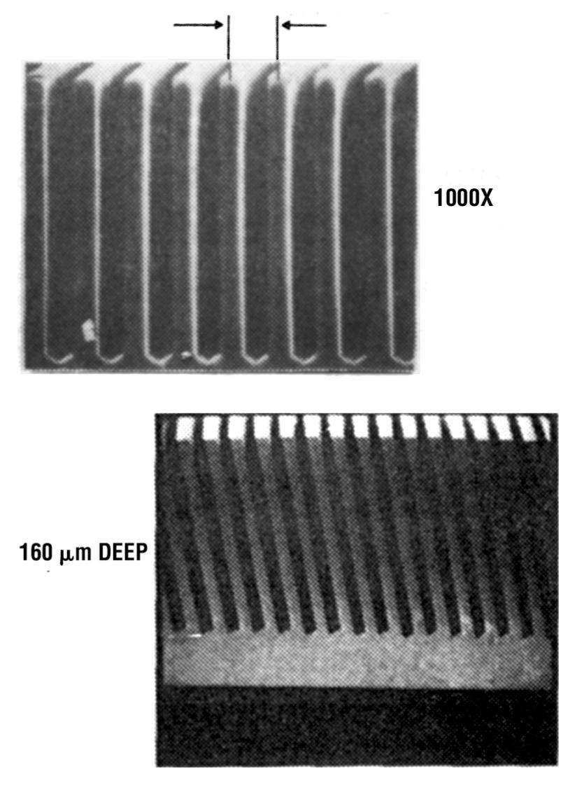
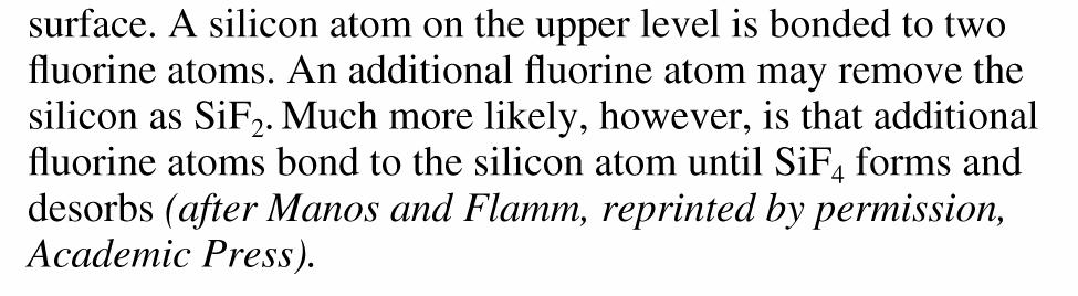
27 High pressure plasma etching In CF4 plasma, small ion concentration, etch is not directly due to ions in plasma. Rather ion bombardment on surface creates unsatisfied bond that are exposed to reactive radicals. Form volatile products and are pumped away. At wafer surface, Si atom is bonded to 2 F atoms. Both SiF2 and SiF4 are volatile species, but SiF2 will not readily desorb since it is chemically bonded to wafer. 27
28 28
29 Plasma etching Possible to use F2 as feed gas, but high toxicity Preferred species are CF4, C2F6, SF6, produce large concentrations of free F. Addition of small concentrations of O2 to a CF4 feed gas increase etch rate of Si and SiO2. O2 reacts with C to produce CO2. this removes C from plasma, increase F concentration. 29
30 30

31 Anisotropic etch: fluorocarbons deposit on all surfaces. Ion velocity, which follows electric field, is vertical. Little ion bombardment on sidewall, fluorocarbon accumulates Process of producing non-volatile species that reduce etch rate is polymerization The film is said to passivate sidewall, prevent lateral etching 31
32 32
33 Ion milling Pure ion milling/ion beam etching: no chemical reactions, since it uses noble gases such as argon. A strictly mechanical process Advantages: Directionality: ions are accelerated by a strong electric field, chamber pressure is low that atomic collision is not likely. Anisotropic etching is possible for any material since it is chemistry independent Applicability: it can be used to pattern a wide variety of materials including compounds and alloys 33
34 Kaufman source Most popular source of ion milling Electron filament heated using supply V F. Filament is held at a voltage Va below anode potential. Electron boil off of filament and are accelerated toward anode. Electrons impact neutral the neutral gas atoms to ionize them. To maintain plasma, source is held at torr. 34
35 Kaufman source A grid held at Vg accelerates ejected ions toward target Ejected ions enter target chamber To maintain directional etch, target chamber is pumped to low pressure, minimize collisions between ions and residual gas molecules 35
36 Ion beam milling Ions are positively charged, a voltage will build up on the surface unless wafer and film being etched are conductive To avoid charging effect, electron flood gun is used 36
37 Problems of ion beam milling Process erode mask layer, any taper in masking layer be transferred to pattern Eroded material from target is not volatile. Some will redeposit on wafer surface, lead to uneven etch and organic residue from resist mask. Trenching: mask erosion causes sidewalls of the pattern to be tapered at a steep angle. Some of low angle ions will reflect off of tapered surface toward the pattern edge 37
38 Ion beam milling An inert species such as argon can be mixed with small amounts of oxygen to reduce erosion rate of many metals in an ion mill. Introducing reactive species tend to attack source components. In particular, hot filament is attacked. 38
39 Reactive ion etching Need for anisotropic etch with higher selectivity than ion milling 39

40 Two common systems for RIE Chlorine plasma for anisotropically Si, GaAs, Al etch 40
41 Undoped Si etch slowly in Cl/Cl2 ambient without addition of ion bombardment Heavily n-type doped Si etches without bombardment in Cl, but not in Cl2. Doping implies that Cl etching involves electron transfer from substrate Chlorine RIE 41
42 Chlorine RIE model Atomic Cl chemisorbs on Si. Once surface Cl becomes negatively charged, it can bond ionically with the substrate. This frees additional chemisorption sites and increases probability that Cl atoms penetrate surface and produce volatile silicon chlorides. 42
43 Cl RIE Cl penetration is increased by ion bombardment Charge transfer produces isotropic etch in heavily doped layers such as polysi gates and Al metallizations. In these structures, obtain anisotropic etch by sidewall polymerization. Sidewall polymerization is done by adjusting relative concentrations of Cl2 and BCl3, CCl4 or SiCl4. 43
44 Damage in RIE Residual damage after RIE: physical damage chemical damage 44

45 Physical Damage in RIE Etch of SiO2 down to Si: surface is damaged with an extensive concentration of Si-O, Si-C bonds. H2 penetration can deactivate dopants in substrate. 45
46 Chemical Damage in RIE a concern in polymerization etches, leave behind residual films Gas particle deposition Metallic impurities due to sputtering of electrodes, chamber, fixture in contact with plasms 46
47 High-Density Plasma (HDP) etching High-density sources use crossed magnetic and electric fields to increase distance the free electrons in plasma travel. This, in turn, increase rate of dissociation and ionization. High density of ions and radicals can be used to increase etch rate. 47

48 High-Density Plasma (HDP) etching A HDP system: inductively coupled reactor, use RF current through coils to produce an oscillating magnetic field that creates an electric field. This induced magnetic field alters path of electrons in plasmas, increase plasma density. 48
49 liftoff An alternative to ion milling for patterning difficult to etch materials 49
50 Procedure of liftoff Resist is spun and patterned 50
51 Procedure of liftoff A thin layer of meal is deposited using evaporation. Evaporation: difficult in covering high aspect ratio features. If a reentrant profile is obtained in resist, a break in metal is assured. 51
52 Procedure of liftoff Wafer is immersed n a solution to dissolve resist. 52
53 Procedure of liftoff To form a reentrant angle by hardening resist surface. Soak DQN resist after softbake in chlorobenzene to reduce dissolution rate of upper surface of resist. After developing, a ledge appears. 53
54 Shortcoming of liftoff Surface topology must be smooth, since metal deposition step has poor step coverage. Metal lifted off remains solid and floats in bath. Pieces of it are likely to redeposit on wafer surface. 54
CHAPTER 6: Etching. Chapter 6 1
 Chapter 6 1 CHAPTER 6: Etching Different etching processes are selected depending upon the particular material to be removed. As shown in Figure 6.1, wet chemical processes result in isotropic etching
Section 3: Etching. Jaeger Chapter 2 Reader
 Section 3: Etching Jaeger Chapter 2 Reader Etch rate Etch Process - Figures of Merit Etch rate uniformity Selectivity Anisotropy d m Bias and anisotropy etching mask h f substrate d f d m substrate d f
Wet and Dry Etching. Theory
 Wet and Dry Etching Theory 1. Introduction Etching techniques are commonly used in the fabrication processes of semiconductor devices to remove selected layers for the purposes of pattern transfer, wafer
Lecture 11. Etching Techniques Reading: Chapter 11. ECE Dr. Alan Doolittle
 Lecture 11 Etching Techniques Reading: Chapter 11 Etching Techniques Characterized by: 1.) Etch rate (A/minute) 2.) Selectivity: S=etch rate material 1 / etch rate material 2 is said to have a selectivity
ETCHING Chapter 10. Mask. Photoresist
 ETCHING Chapter 10 Mask Light Deposited Substrate Photoresist Etch mask deposition Photoresist application Exposure Development Etching Resist removal Etching of thin films and sometimes the silicon substrate
EE 527 MICROFABRICATION. Lecture 25 Tai-Chang Chen University of Washington
 EE 527 MICROFABRICATION Lecture 25 Tai-Chang Chen University of Washington ION MILLING SYSTEM Kaufmann source Use e-beam to strike plasma A magnetic field applied to increase ion density Drawback Low etch
4FNJDPOEVDUPS 'BCSJDBUJPO &UDI
 2010.5.4 1 Major Fabrication Steps in CMOS Process Flow UV light oxygen Silicon dioxide Silicon substrate Oxidation (Field oxide) photoresist Photoresist Coating Mask exposed photoresist Mask-Wafer Exposed
Etching: Basic Terminology
 Lecture 7 Etching Etching: Basic Terminology Introduction : Etching of thin films and sometimes the silicon substrate are very common process steps. Usually selectivity, and directionality are the first
UNIT 3. By: Ajay Kumar Gautam Asst. Prof. Dev Bhoomi Institute of Technology & Engineering, Dehradun
 UNIT 3 By: Ajay Kumar Gautam Asst. Prof. Dev Bhoomi Institute of Technology & Engineering, Dehradun 1 Syllabus Lithography: photolithography and pattern transfer, Optical and non optical lithography, electron,
Device Fabrication: Etch
 Device Fabrication: Etch 1 Objectives Upon finishing this course, you should able to: Familiar with etch terminology Compare wet and dry etch processes processing and list the main dry etch etchants Become
EE 527 MICROFABRICATION. Lecture 24 Tai-Chang Chen University of Washington
 EE 527 MICROFABRICATION Lecture 24 Tai-Chang Chen University of Washington EDP ETCHING OF SILICON - 1 Ethylene Diamine Pyrocatechol Anisotropy: (100):(111) ~ 35:1 EDP is very corrosive, very carcinogenic,
Reactive Ion Etching (RIE)
") Reactive Ion Etching (RIE) RF 13.56 ~ MHz plasma Parallel-Plate Reactor wafers Sputtering Plasma generates (1) Ions (2) Activated neutrals Enhance chemical reaction 1 2 Remote Plasma Reactors Plasma Sources
Reactive Ion Etching (RIE) RF 13.56 ~ MHz plasma Parallel-Plate Reactor wafers Sputtering Plasma generates (1) Ions (2) Activated neutrals Enhance chemical reaction 1 2 Remote Plasma Reactors Plasma Sources
Lecture 15 Etching. Chapters 15 & 16 Wolf and Tauber. ECE611 / CHE611 Electronic Materials Processing Fall John Labram 1/76
 Lecture 15 Etching Chapters 15 & 16 Wolf and Tauber 1/76 Announcements Term Paper: You are expected to produce a 4-5 page term paper on a selected topic (from a list). Term paper contributes 25% of course
Dry Etching Zheng Yang ERF 3017, MW 5:15-6:00 pm
 Dry Etching Zheng Yang ERF 3017, email: yangzhen@uic.edu, MW 5:15-6:00 pm Page 1 Page 2 Dry Etching Why dry etching? - WE is limited to pattern sizes above 3mm - WE is isotropic causing underetching -
Etching Issues - Anisotropy. Dry Etching. Dry Etching Overview. Etching Issues - Selectivity
 Etching Issues - Anisotropy Dry Etching Dr. Bruce K. Gale Fundamentals of Micromachining BIOEN 6421 EL EN 5221 and 6221 ME EN 5960 and 6960 Isotropic etchants etch at the same rate in every direction mask
LECTURE 5 SUMMARY OF KEY IDEAS
 LECTURE 5 SUMMARY OF KEY IDEAS Etching is a processing step following lithography: it transfers a circuit image from the photoresist to materials form which devices are made or to hard masking or sacrificial
Chapter 7 Plasma Basic
 Chapter 7 Plasma Basic Hong Xiao, Ph. D. hxiao89@hotmail.com www2.austin.cc.tx.us/hongxiao/book.htm Hong Xiao, Ph. D. www2.austin.cc.tx.us/hongxiao/book.htm 1 Objectives List at least three IC processes
Plasma Deposition (Overview) Lecture 1
 Lecture 1") Plasma Deposition (Overview) Lecture 1 Material Processes Plasma Processing Plasma-assisted Deposition Implantation Surface Modification Development of Plasma-based processing Microelectronics needs (fabrication
Plasma Deposition (Overview) Lecture 1 Material Processes Plasma Processing Plasma-assisted Deposition Implantation Surface Modification Development of Plasma-based processing Microelectronics needs (fabrication
CVD: General considerations.
 CVD: General considerations. PVD: Move material from bulk to thin film form. Limited primarily to metals or simple materials. Limited by thermal stability/vapor pressure considerations. Typically requires
Chapter 7. Plasma Basics
 Chapter 7 Plasma Basics 2006/4/12 1 Objectives List at least three IC processes using plasma Name three important collisions in plasma Describe mean free path Explain how plasma enhance etch and CVD processes
E SC 412 Nanotechnology: Materials, Infrastructure, and Safety Wook Jun Nam
 E SC 412 Nanotechnology: Materials, Infrastructure, and Safety Wook Jun Nam Lecture 10 Outline 1. Wet Etching/Vapor Phase Etching 2. Dry Etching DC/RF Plasma Plasma Reactors Materials/Gases Etching Parameters
Lecture 6 Plasmas. Chapters 10 &16 Wolf and Tauber. ECE611 / CHE611 Electronic Materials Processing Fall John Labram 1/68
 Lecture 6 Plasmas Chapters 10 &16 Wolf and Tauber 1/68 Announcements Homework: Homework will be returned to you on Thursday (12 th October). Solutions will be also posted online on Thursday (12 th October)
Outline. 1 Introduction. 2 Basic IC fabrication processes. 3 Fabrication techniques for MEMS. 4 Applications. 5 Mechanics issues on MEMS 1 MDL NTHU
 Outline 1 Introduction 2 Basic IC fabrication processes 3 Fabrication techniques for MEMS 4 Applications 5 Mechanics issues on MEMS 1 MDL 2. Basic IC fabrication processes 2.1 Deposition and growth 2.2
Metal Deposition. Filament Evaporation E-beam Evaporation Sputter Deposition
 Metal Deposition Filament Evaporation E-beam Evaporation Sputter Deposition 1 Filament evaporation metals are raised to their melting point by resistive heating under vacuum metal pellets are placed on
Plasma etching. Bibliography
 Plasma etching Bibliography 1. B. Chapman, Glow discharge processes, (Wiley, New York, 1980). - Classical plasma processing of etching and sputtering 2. D. M. Manos and D. L. Flamm, Plasma etching; An
Etching. Etching Terminology. Etching Considerations for ICs. Wet Etching. Reactive Ion Etching (plasma etching) Professor N Cheung, U.C.
 Professor N Cheung, U.C.") Etching Etching Terminology Etching Considerations or ICs Wet Etching Reactie Ion Etching (plasma etching) 1 Etch Process - Figures o Merit Etch rate Etch rate uniormity Selectiity Anisotropy 2 (1) Bias
Etching Etching Terminology Etching Considerations or ICs Wet Etching Reactie Ion Etching (plasma etching) 1 Etch Process - Figures o Merit Etch rate Etch rate uniormity Selectiity Anisotropy 2 (1) Bias
Self-study problems and questions Processing and Device Technology, FFF110/FYSD13
 Self-study problems and questions Processing and Device Technology, FFF110/FYSD13 Version 2016_01 In addition to the problems discussed at the seminars and at the lectures, you can use this set of problems
EE C245 ME C218 Introduction to MEMS Design Fall 2010
 Lecture Outline EE C245 ME C28 Introduction to MEMS Design Fall 200 Prof. Clark T.-C. Nguyen Dept. of Electrical Engineering & Computer Sciences University of California at Berkeley Berkeley, CA 94720
Regents of the University of California
 Deep Reactive-Ion Etching (DRIE) DRIE Issues: Etch Rate Variance The Bosch process: Inductively-coupled plasma Etch Rate: 1.5-4 μm/min Two main cycles in the etch: Etch cycle (5-15 s): SF 6 (SF x+ ) etches
Lithography and Etching
 Lithography and Etching Victor Ovchinnikov Chapters 8.1, 8.4, 9, 11 Previous lecture Microdevices Main processes: Thin film deposition Patterning (lithography) Doping Materials: Single crystal (monocrystal)
Introduction to Photolithography
 http://www.ichaus.de/news/72 Introduction to Photolithography Photolithography The following slides present an outline of the process by which integrated circuits are made, of which photolithography is
ELEC 7364 Lecture Notes Summer Etching. by STELLA W. PANG. from The University of Michigan, Ann Arbor, MI, USA
 ELEC 7364 Lecture Notes Summer 2008 Etching by STELLA W. PANG from The University of Michigan, Ann Arbor, MI, USA Visiting Professor at The University of Hong Kong The University of Michigan on Visiting
TMT4320 Nanomaterials November 10 th, Thin films by physical/chemical methods (From chapter 24 and 25)
") 1 TMT4320 Nanomaterials November 10 th, 2015 Thin films by physical/chemical methods (From chapter 24 and 25) 2 Thin films by physical/chemical methods Vapor-phase growth (compared to liquid-phase growth)
1 TMT4320 Nanomaterials November 10 th, 2015 Thin films by physical/chemical methods (From chapter 24 and 25) 2 Thin films by physical/chemical methods Vapor-phase growth (compared to liquid-phase growth)
Chapter 9, Etch. Hong Xiao, Ph. D. www2.austin.cc.tx.us/hongxiao/book.htm
 Chapter 9, Etch Hong Xiao, Ph. D. hxiao89@hotmail.com www2.austin.cc.tx.us/hongxiao/book.htm Hong Xiao, Ph. D. www2.austin.cc.tx.us/hongxiao/book.htm 1 Objectives Upon finishing this course, you should
EE C245 ME C218 Introduction to MEMS Design Fall 2007
 EE C245 ME C218 Introduction to MEMS Design Fall 2007 Prof. Clark T.-C. Nguyen Dept. of Electrical Engineering & Computer Sciences University of California at Berkeley Berkeley, CA 94720 Lecture 12: Mechanics
Introduction to Plasma
 What is a plasma? The fourth state of matter A partially ionized gas How is a plasma created? Energy must be added to a gas in the form of: Heat: Temperatures must be in excess of 4000 O C Radiation Electric
Technology for Micro- and Nanostructures Micro- and Nanotechnology
 Lecture 10: Deposition Technology for Micro- and Nanostructures Micro- and Nanotechnology Peter Unger mailto: peter.unger @ uni-ulm.de Institute of Optoelectronics University of Ulm http://www.uni-ulm.de/opto
UNIVERSITY OF CALIFORNIA College of Engineering Department of Electrical Engineering and Computer Sciences. Fall Exam 1
 UNIVERSITY OF CALIFORNIA College of Engineering Department of Electrical Engineering and Computer Sciences EECS 143 Fall 2008 Exam 1 Professor Ali Javey Answer Key Name: SID: 1337 Closed book. One sheet
DEPOSITION OF THIN TiO 2 FILMS BY DC MAGNETRON SPUTTERING METHOD
 Chapter 4 DEPOSITION OF THIN TiO 2 FILMS BY DC MAGNETRON SPUTTERING METHOD 4.1 INTRODUCTION Sputter deposition process is another old technique being used in modern semiconductor industries. Sputtering
EE C245 ME C218 Introduction to MEMS Design
 EE C245 ME C218 Introduction to MEMS Design Fall 2008 Prof. Clark T.-C. Nguyen Dept. of Electrical Engineering & Computer Sciences University of California at Berkeley Berkeley, CA 94720 Lecture 6: Process
Chapter 8 Ion Implantation
 Chapter 8 Ion Implantation 2006/5/23 1 Wafer Process Flow Materials IC Fab Metalization CMP Dielectric deposition Test Wafers Masks Thermal Processes Implant PR strip Etch PR strip Packaging Photolithography
EE C245 ME C218 Introduction to MEMS Design Fall 2007
 EE C245 ME C218 Introduction to MEMS Design Fall 2007 Prof. Clark T.-C. Nguyen Dept. of Electrical Engineering & Computer Sciences University of California at Berkeley Berkeley, CA 94720 Lecture 11: Bulk
EE C245 ME C218 Introduction to MEMS Design Fall 2007
 EE C245 ME C218 Introduction to MEMS Design Fall 2007 Prof. Clark T.-C. Nguyen Dept. of Electrical Engineering & Computer Sciences University of California at Berkeley Berkeley, CA 94720 Lecture 4: Film
Thin Film Deposition. Reading Assignments: Plummer, Chap 9.1~9.4
 Thin Film Deposition Reading Assignments: Plummer, Chap 9.1~9.4 Thermally grown Deposition Thin Film Formation Thermally grown SiO 2 Deposition SiO 2 Oxygen is from gas phase Silicon from substrate Oxide
MICROCHIP MANUFACTURING by S. Wolf
 by S. Wolf Chapter 15 ALUMINUM THIN-FILMS and SPUTTER-DEPOSITION 2004 by LATTICE PRESS CHAPTER 15 - CONTENTS Aluminum Thin-Films Sputter-Deposition Process Steps Physics of Sputter-Deposition Magnetron-Sputtering
YEAR 10- Chemistry Term 1 plan
 YEAR 10- Chemistry Term 1 plan 2016-2017 Week Topic Learning outcomes 1 1. The particulate nature of matter State the distinguishing properties of solids, liquids and gases. Describe the structure of solids,
Clean-Room microfabrication techniques. Francesco Rizzi Italian Institute of Technology
 Clean-Room microfabrication techniques Francesco Rizzi Italian Institute of Technology Miniaturization The first transistor Miniaturization The first transistor Miniaturization The first transistor Miniaturization
3.155J/6.152J Microelectronic Processing Technology Fall Term, 2004
 3.155J/6.152J Microelectronic Processing Technology Fall Term, 2004 Bob O'Handley Martin Schmidt Quiz Nov. 17, 2004 Ion implantation, diffusion [15] 1. a) Two identical p-type Si wafers (N a = 10 17 cm
EE-612: Lecture 22: CMOS Process Steps
 EE-612: Lecture 22: CMOS Process Steps Mark Lundstrom Electrical and Computer Engineering Purdue University West Lafayette, IN USA Fall 2006 NCN www.nanohub.org Lundstrom EE-612 F06 1 outline 1) Unit Process
Fabrication Technology, Part I
 EEL5225: Principles of MEMS Transducers (Fall 2004) Fabrication Technology, Part I Agenda: Microfabrication Overview Basic semiconductor devices Materials Key processes Oxidation Thin-film Deposition Reading:
Lecture 150 Basic IC Processes (10/10/01) Page ECE Analog Integrated Circuits and Systems P.E. Allen
 Page ECE Analog Integrated Circuits and Systems P.E. Allen") Lecture 150 Basic IC Processes (10/10/01) Page 1501 LECTURE 150 BASIC IC PROCESSES (READING: TextSec. 2.2) INTRODUCTION Objective The objective of this presentation is: 1.) Introduce the fabrication of
Lecture 150 Basic IC Processes (10/10/01) Page 1501 LECTURE 150 BASIC IC PROCESSES (READING: TextSec. 2.2) INTRODUCTION Objective The objective of this presentation is: 1.) Introduce the fabrication of
EE143 Fall 2016 Microfabrication Technologies. Lecture 6: Thin Film Deposition Reading: Jaeger Chapter 6
 EE143 Fall 2016 Microfabrication Technologies Lecture 6: Thin Film Deposition Reading: Jaeger Chapter 6 Prof. Ming C. Wu wu@eecs.berkeley.edu 511 Sutardja Dai Hall (SDH) 1 Vacuum Basics Units 1 atmosphere
Semiconductor Technology
 Semiconductor Technology from A to Z Deposition www.halbleiter.org Contents Contents List of Figures II 1 Deposition 1 1.1 Plasma, the fourth aggregation state of a material............. 1 1.1.1 Plasma
6.5 Optical-Coating-Deposition Technologies
 92 Chapter 6 6.5 Optical-Coating-Deposition Technologies The coating process takes place in an evaporation chamber with a fully controlled system for the specified requirements. Typical systems are depicted
Introduction to Thin Film Processing
 Introduction to Thin Film Processing Deposition Methods Many diverse techniques available Typically based on three different methods for providing a flux of atomic or molecular material Evaporation Sputtering
Film Deposition Part 1
 1 Film Deposition Part 1 Chapter 11 : Semiconductor Manufacturing Technology by M. Quirk & J. Serda Spring Semester 2013 Saroj Kumar Patra Semidonductor Manufacturing Technology, Norwegian University of
Ion Implant Part 1. Saroj Kumar Patra, TFE4180 Semiconductor Manufacturing Technology. Norwegian University of Science and Technology ( NTNU )
") 1 Ion Implant Part 1 Chapter 17: Semiconductor Manufacturing Technology by M. Quirk & J. Serda Spring Semester 2014 Saroj Kumar Patra,, Norwegian University of Science and Technology ( NTNU ) 2 Objectives
1 Ion Implant Part 1 Chapter 17: Semiconductor Manufacturing Technology by M. Quirk & J. Serda Spring Semester 2014 Saroj Kumar Patra,, Norwegian University of Science and Technology ( NTNU ) 2 Objectives
DQN Positive Photoresist
 UNIVESITY OF CALIFONIA, BEKELEY BEKELEY DAVIS IVINE LOS ANGELES IVESIDE SAN DIEGO SAN FANCISCO SANTA BABAA SANTA CUZ DEPATMENT OF BIOENGINEEING 94720-1762 BioE 121 Midterm #1 Solutions BEKELEY, CALIFONIA
Outlines 3/12/2011. Vacuum Chamber. Inside the sample chamber. Nano-manipulator. Focused ion beam instrument. 1. Other components of FIB instrument
 Focused ion beam instruments Outlines 1. Other components of FIB instrument 1.a Vacuum chamber 1.b Nanomanipulator 1.c Gas supply for deposition 1.d Detectors 2. Capabilities of FIB instrument Lee Chow
40S CHEMISTRY FINAL EXAM PROBLEM REVIEW SHEET:
 40S CHEMISTRY FINAL EXAM PROBLEM REVIEW SHEET: **THIS IS NOT A COMPLETE REVIEW. CONTINUE TO READ ALL COURSE NOTES, GO OVER ALL WORKSHEETS, HANDOUTS, AND THE UNIT TESTS TO BE BETTER PREPARED. To prepare
Chapter 3 Engineering Science for Microsystems Design and Fabrication
 Lectures on MEMS and MICROSYSTEMS DESIGN and MANUFACTURE Chapter 3 Engineering Science for Microsystems Design and Fabrication In this Chapter, we will present overviews of the principles of physical and
Name:. Correct Questions = Wrong Questions =.. Unattempt Questions = Marks =
 Name:. Correct Questions = Wrong Questions =.. Unattempt Questions = Marks = 1. (12%) Compound X contains 2.239% hydrogen, 26.681% carbon and 71.080 % oxygen by mass. The titration of 0.154 g of this compound
Lecture 16 Chemical Mechanical Planarization
 Lecture 16 Chemical Mechanical Planarization 1/75 Announcements Term Paper: The term paper should be handed in today: Tuesday 21 st November. The term paper will be returned to you in class on Tuesday
Repetition: Practical Aspects
 Repetition: Practical Aspects Reduction of the Cathode Dark Space! E x 0 Geometric limit of the extension of a sputter plant. Lowest distance between target and substrate V Cathode (Target/Source) - +
CHEMISTRY. SCIENCE Paper 2
 CHEMISTRY SCIENCE Paper 2 (Two hours) Answers to this Paper must be written on the paper provided separately. You will not be allowed to write during the first 15 minutes. This time is to be spent in reading
MAHESH TUTORIALS I.C.S.E.
 MAHESH TUTORIALS I.C.S.E. GRADE - X (2017-2018) Exam No. : MT/ICSE/SEMI PRELIM - I-SET -A 008 Sulphuric acid, Ammonia, Analytical Chemistry, Organic Chemistry HCl, Nitric acid, Metallurgy Chemistry SCIENCE
40S CHEMISTRY FINAL EXAM PROBLEM REVIEW SHEET:
 40S CHEMISTRY FINAL EXAM PROBLEM REVIEW SHEET: **THIS IS NOT A COMPLETE REVIEW. CONTINUE TO READ ALL COURSE NOTES, GO OVER ALL WORKSHEETS, HANDOUTS, AND THE MID-TERM EXAM TO BE BETTER PREPARED. To prepare
Chapter 6. Chemical Reactions. Sodium reacts violently with bromine to form sodium bromide.
 Chapter 6 Chemical Reactions Sodium reacts violently with bromine to form sodium bromide. Evidence of Chemical Reactions Chemical Equations Reactants Products Reactant(s): Substance(s) present before the
Copyright Warning & Restrictions
 Copyright Warning & Restrictions The copyright law of the United States (Title 17, United States Code) governs the making of photocopies or other reproductions of copyrighted material. Under certain conditions
ECE611 / CHE611: Electronic Materials Processing Fall 2017 John Labram Solutions to Homework 2 Due at the beginning of class Thursday October 19 th
 ECE611 / CHE611: Electronic Materials Processing Fall 017 John Labram Solutions to Homework Due at the beginning of class Thursday October 19 th Question 1 [3 marks]: a) Piranha solution consists of a
DEPOSITION AND COMPOSITION OF POLYMER FILMS IN FLUOROCARBON PLASMAS*
 DEPOSITION AND COMPOSITION OF POLYMER FILMS IN FLUOROCARBON PLASMAS* Kapil Rajaraman and Mark J. Kushner 1406 W. Green St. Urbana, IL 61801 rajaramn@uiuc.edu mjk@uiuc.edu http://uigelz.ece.uiuc.edu November
Answers for UNIT ONE NAT 5 Flash Cards
 Answers for UNIT ONE NAT 5 Flash Cards 1. (a) rate increases (b) rate increases (c) rate increases (d) rate increases 2. Average rate = change in property / change in time Where property = concentration,
Secondary ion mass spectrometry (SIMS)
") Secondary ion mass spectrometry (SIMS) ELEC-L3211 Postgraduate Course in Micro and Nanosciences Department of Micro and Nanosciences Personal motivation and experience on SIMS Offers the possibility to
Secondary ion mass spectrometry (SIMS) ELEC-L3211 Postgraduate Course in Micro and Nanosciences Department of Micro and Nanosciences Personal motivation and experience on SIMS Offers the possibility to
Supplementary Figure 1 Detailed illustration on the fabrication process of templatestripped
 Supplementary Figure 1 Detailed illustration on the fabrication process of templatestripped gold substrate. (a) Spin coating of hydrogen silsesquioxane (HSQ) resist onto the silicon substrate with a thickness
Spring Lecture 4 Contamination Control and Substrate Cleaning. Nanometer Scale Patterning and Processing
 Nanometer Scale Patterning and Processing Spring 2016 Lecture 4 Contamination Control and Substrate Cleaning Contaminants A substance causes uncontrolled variations in the (electrical) performance of the
Figure 1: Graphene release, transfer and stacking processes. The graphene stacking began with CVD
 Supplementary figure 1 Graphene Growth and Transfer Graphene PMMA FeCl 3 DI water Copper foil CVD growth Back side etch PMMA coating Copper etch in 0.25M FeCl 3 DI water rinse 1 st transfer DI water 1:10
CHEM 200/202. Professor Gregory P. Holland Office: GMCS-213C. All s are to be sent to:
 CHEM 200/202 Professor Gregory P. Holland Office: GMCS-213C All emails are to be sent to: chem200@mail.sdsu.edu My office hours will be held in GMCS-212 on Monday from 12:00 pm to 2:00 pm or by appointment.
Photoresist Profile. Undercut: negative slope, common for negative resist; oxygen diffusion prohibits cross-linking; good for lift-off.
 Photoresist Profile 4-15 Undercut: negative slope, common for negative resist; oxygen diffusion prohibits cross-linking; good for lift-off undercut overcut Overcut: positive slope, common to positive resist,
Chem 12: Chapters 10, 11, 12, 13, 14 Unit 3 Worksheet
 C h e m i s t r y 1 2 U n i t 3 R e v i e w P a g e 1 Chem 12: Chapters 10, 11, 12, 13, 14 Unit 3 Worksheet 1. What is miscible? Immiscible? 2. What is saturated? Unsaturated? Supersaturated? 3. How does
[2]... [1]
![[2]... [1]](/thumbs/75/71765689.jpg "[2]... [1]") 1 Carbon and silicon are elements in Group IV. Both elements have macromolecular structures. (a) Diamond and graphite are two forms of the element carbon. (i) Explain why diamond is a very hard substance....
1 Carbon and silicon are elements in Group IV. Both elements have macromolecular structures. (a) Diamond and graphite are two forms of the element carbon. (i) Explain why diamond is a very hard substance....
CHEM 200/202. Professor Jing Gu Office: EIS-210. All s are to be sent to:
 CHEM 200/202 Professor Jing Gu Office: EIS-210 All emails are to be sent to: chem200@mail.sdsu.edu My office hours will be held in GMCS-212 on Monday from 9 am to 11 am or by appointment. ANNOUNCEMENTS
GCSE OCR Revision Chemistry. GCSE OCR Revision Chemistry. GCSE OCR Revision Chemistry. Bonding. GCSE OCR Revision Chemistry
 Particle Model and Atomic Structure The following symbols describe two different substances. Deduce all the information you can from these symbols. 13 C 12 6 6 C 1 Particle Model and Atomic Structure The
Chapter Two (Chemistry of Life)
") 1 Chapter Two (Chemistry of Life) SECTION ONE: THE COMPOSITION OF MATTER MATTER Everything in the universe is made of matter. Matter is anything that occupies space and has mass. Mass is the quantity of
1 Chapter Two (Chemistry of Life) SECTION ONE: THE COMPOSITION OF MATTER MATTER Everything in the universe is made of matter. Matter is anything that occupies space and has mass. Mass is the quantity of
EXPERIMENTS. Testing products of combustion: Reducing Copper(III) Oxide to Copper. Page 4
 Oxide to Copper. Page 4") APPARATUS Page 2 APPARATUS Page 3 Reducing Copper(III) Oxide to Copper EXPERIMENTS Page 4 Testing products of combustion: EXPERIMENTS Showing that oxygen and water is needed for rusting iron Page 5 Showing
APPARATUS Page 2 APPARATUS Page 3 Reducing Copper(III) Oxide to Copper EXPERIMENTS Page 4 Testing products of combustion: EXPERIMENTS Showing that oxygen and water is needed for rusting iron Page 5 Showing
Conductivity of Electrolytes in Solution
 Conductivity of Electrolytes in Solution Introduction: Electrical current can be thought of as the movement of electrons or ionic charges from an area of high potential to an area of low potential. Materials
CHEMISTRY 2b SUMMARY
 CHEMISTRY 2b SUMMARY Items in ITALLICS are HIGHER TIER NLY C2.4.1 RATES F REACTIN Speeding up, or slowing down, chemical reactions is important in everyday life and in industry The rate of a chemical reaction
Kenya Certificate of Secondary Education (K.C.S.E.)
") Name: Index No. School:. Candidate s Sign.... Date:... 233/1 CHEMISTRY PAPER 1 JULY /AUGUST 2011 TIME: 2 HOURS Kenya Certificate of Secondary Education (K.C.S.E.) Chemistry Paper 1 INSTRUCTIONS TO THE
Name: Index No. School:. Candidate s Sign.... Date:... 233/1 CHEMISTRY PAPER 1 JULY /AUGUST 2011 TIME: 2 HOURS Kenya Certificate of Secondary Education (K.C.S.E.) Chemistry Paper 1 INSTRUCTIONS TO THE
Based on the kinetic molecular theory of gases, which one of the following statements is INCORRECT?
 1 Based on the kinetic molecular theory of gases, which one of the following statements is INCORRECT? A) The collisions between gas molecules are perfectly elastic. B) At absolute zero, the average kinetic
Numerical Simulation: Effects of Gas Flow and Rf Current Direction on Plasma Uniformity in an ICP Dry Etcher
 Appl. Sci. Converg. Technol. 26(6): 189-194 (2017) http://dx.doi.org/10.5757/asct.2017.26.6.189 Research Paper Numerical Simulation: Effects of Gas Flow and Rf Current Direction on Plasma Uniformity in
Section 5: Thin Film Deposition part 1 : sputtering and evaporation. Jaeger Chapter 6. EE143 Ali Javey
 Section 5: Thin Film Deposition part 1 : sputtering and evaporation Jaeger Chapter 6 Vacuum Basics 1. Units 1 atmosphere = 760 torr = 1.013x10 5 Pa 1 bar = 10 5 Pa = 750 torr 1 torr = 1 mm Hg 1 mtorr =
Repetition: Ion Plating
 Repetition: Ion Plating Substrate HV (bis ca. 1kV) Optional ionization system Source Ionized filling gas Source material, ionized or neutral Repetition: Ion Plating Ion Species Separated ion source Ions
IGCSE(A*-G) Edexcel - Chemistry
 Edexcel - Chemistry") IGCSE(A*-G) Edexcel - Chemistry Principles of Chemistry Atoms NOTES 1.8 Describe and explain experiments to investigate the small size of particles and their movement including: Dilution of coloured solutions
IGCSE(A*-G) Edexcel - Chemistry Principles of Chemistry Atoms NOTES 1.8 Describe and explain experiments to investigate the small size of particles and their movement including: Dilution of coloured solutions
ION Pumps for UHV Systems, Synchrotrons & Particle Accelerators. Mauro Audi, Academic, Government & Research Marketing Manager
 ION Pumps for UHV Systems, Synchrotrons & Particle Accelerators Mauro Audi, Academic, Government & Research Marketing Manager ION Pumps Agilent Technologies 1957-59 Varian Associates invents the first
AP Chemistry Review Packet #3
 AP Chemistry Review Packet #3 Warmup Given the reaction N 2 O 3(g) NO (g) + NO 2(g) H = +39.7 kj, predict the effect that each of the following changes will have on the given values N 2 O 3 NO NO 2 Keq
molality: m = = 1.70 m
 C h e m i s t r y 1 2 U n i t 3 R e v i e w P a g e 1 Chem 12: Chapters 10, 11, 12, 13, 14 Unit 3 Worksheet 1. What is miscible? Immiscible? Miscible: two or more substances blend together for form a solution
MODELING OF SEASONING OF REACTORS: EFFECTS OF ION ENERGY DISTRIBUTIONS TO CHAMBER WALLS*
 MODELING OF SEASONING OF REACTORS: EFFECTS OF ION ENERGY DISTRIBUTIONS TO CHAMBER WALLS* Ankur Agarwal a) and Mark J. Kushner b) a) Department of Chemical and Biomolecular Engineering University of Illinois,
A covalent bond is a shared pair of electrons between atoms of two non-metal elements.
 Bonding, Structure and properties Atoms can be held together by chemical bonds. When atoms form bonds, they can achieve a stable electron arrangement (full outer electron shell). To achieve a stable electron
Stoichiometry: Chemical Calculations. Chemistry is concerned with the properties and the interchange of matter by reaction i.e. structure and change.
 Chemistry is concerned with the properties and the interchange of matter by reaction i.e. structure and change. In order to do this, we need to be able to talk about numbers of atoms. The key concept is
Ion Implantation. alternative to diffusion for the introduction of dopants essentially a physical process, rather than chemical advantages:
 Ion Implantation alternative to diffusion for the introduction of dopants essentially a physical process, rather than chemical advantages: mass separation allows wide varies of dopants dose control: diffusion
Basic Digestion Principles
 Basic Digestion Principles 1 From Samples to Solutions Direct Analytical Method Solid Sample Problems: Mech. Sample Preparation (Grinding, Sieving, Weighing, Pressing, Polishing,...) Solid Sample Autosampler