Technology for Micro- and Nanostructures Micro- and Nanotechnology
|
|
|
- Cecil Waters
- 5 years ago
- Views:
Transcription
1 Lecture 6: Electron-Beam Lithography, Part 2 Technology for Micro- and Nanostructures Micro- and Nanotechnology Peter Unger mailto: uni-ulm.de Institute of Optoelectronics University of Ulm Copyright 2012 by Peter Unger Peter Unger, Technology for Micro- and Nanostructures Lecture 6: Electron-Beam Lithography, Part 2, Version of November 28, 2012 p. 1/29 Outline of Lectures 5 and 6: E-Beam Lithography Part 1, Lecture 5 Basic Principle of Electron-Beam Lithography The Electron-Optical Column Lens Errors and Beam Size Mark Registration Field Overlay and Stitching Part 2, Lecture 6 Physics of Lenses for Electrons Scatter Effects of Electron Beams The Proximity Correction Peter Unger, Technology for Micro- and Nanostructures Lecture 6: Electron-Beam Lithography, Part 2, Version of November 28, 2012 p. 2/29
2 Basic Principle of Electron-Beam Lithography Peter Unger, Technology for Micro- and Nanostructures Lecture 6: Electron-Beam Lithography, Part 2, Version of November 28, 2012 p. 3/29 Cross Section of an Electron-Optical Column Peter Unger, Technology for Micro- and Nanostructures Lecture 6: Electron-Beam Lithography, Part 2, Version of November 28, 2012 p. 4/29
3 Forces in Electromagnetic Fields Electric Fields Magnetic Fields F = m a = q e E F = m a = q e ( v B) Lorentz Force No Focusing of Electron Beams in Homogeneous Electrostatic and Magnetic Fields Any Axially Symmetric Electrostatic or Magnetic Field has the Property of a Focusing Lens Peter Unger, Technology for Micro- and Nanostructures Lecture 6: Electron-Beam Lithography, Part 2, Version of November 28, 2012 p. 5/29 Electrostatic Electron Einzel Lens Peter Unger, Technology for Micro- and Nanostructures Lecture 6: Electron-Beam Lithography, Part 2, Version of November 28, 2012 p. 6/29

4 Cross Section of a Magnetic Electron Lens Peter Unger, Technology for Micro- and Nanostructures Lecture 6: Electron-Beam Lithography, Part 2, Version of November 28, 2012 p. 7/29 Functioning of a Magnetic Electron Lens Peter Unger, Technology for Micro- and Nanostructures Lecture 6: Electron-Beam Lithography, Part 2, Version of November 28, 2012 p. 8/29
5 Lens Errors in Electron-Beam Optics Peter Unger, Technology for Micro- and Nanostructures Lecture 6: Electron-Beam Lithography, Part 2, Version of November 28, 2012 p. 9/29 Aberation and Diffraction of an Objective Lens Resolution δ δ min Diffraction δ ~ 1/α Sum of Diffraction and Spheric Aberation Spheric Aberation δ ~ α 3 α opt Beam Divergence Angle α Peter Unger, Technology for Micro- and Nanostructures Lecture 6: Electron-Beam Lithography, Part 2, Version of November 28, 2012 p. 10/29

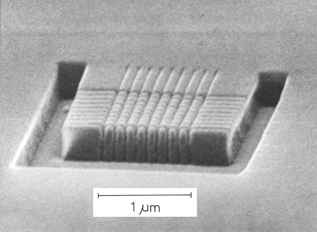
6 Electron-Beam Lithography at 100 kev Resist: PMMA/MAA Substrate: Silicon Peter Unger, Technology for Micro- and Nanostructures Lecture 6: Electron-Beam Lithography, Part 2, Version of November 28, 2012 p. 11/29 Electron-Beam Lithography at 100 kev Resist: PMMA/MAA Substrate: Silicon Peter Unger, Technology for Micro- and Nanostructures Lecture 6: Electron-Beam Lithography, Part 2, Version of November 28, 2012 p. 12/29
 Peter Unger, Technology for Micro- and Nanostructures Lecture 6: Electron-Beam Lithography, Part 2, Version of November 28,")
7 Electron-Beam Lithography at 100 kev Resist: PMMA/MAA Dose: 1 mc/cm 2 Peter Unger, Technology for Micro- and Nanostructures Lecture 6: Electron-Beam Lithography, Part 2, Version of November 28, 2012 p. 13/29 Basic Electron Scattering Mechanisms (after Hersener and Ricker) Peter Unger, Technology for Micro- and Nanostructures Lecture 6: Electron-Beam Lithography, Part 2, Version of November 28, 2012 p. 14/29
8 Double Gaussian Model for the Dose Distribution Peter Unger, Technology for Micro- and Nanostructures Lecture 6: Electron-Beam Lithography, Part 2, Version of November 28, 2012 p. 15/29 The Proximity Function Double Gausssian Model for the Proximity Function f(r) f(r) = k [ exp ( ) r2 βf 2 + η E β2 f β 2 b exp ( )] r2 βb 2 Peter Unger, Technology for Micro- and Nanostructures Lecture 6: Electron-Beam Lithography, Part 2, Version of November 28, 2012 p. 16/29
9 The Proximity Function Double Gausssian Model for the Proximity Function f(r) f(r) = k [ exp ( ) r2 βf 2 β f Forward Scattering Width Broadening of the Electron Beam + η E β2 f β 2 b exp β b Backward Scattering Width Secondary Electron Emission from the Substrate ( )] r2 βb 2 η E Backscatter Coefficient Ratio of Backscattered to Forward Scattered Dose Peter Unger, Technology for Micro- and Nanostructures Lecture 6: Electron-Beam Lithography, Part 2, Version of November 28, 2012 p. 17/29 Monte-Carlo Simulations of the Scattering (after Jones, Blythe, and Ahmed, J. Vac. Sci. Technol. B, vol. 5, pp , 1987) Peter Unger, Technology for Micro- and Nanostructures Lecture 6: Electron-Beam Lithography, Part 2, Version of November 28, 2012 p. 18/29
 Peter Unger, Technology for Micro- and Nanostructures Lecture 6: Electron-Beam Lithography, Part 2, Version of November 28, 2012 p.")
10 Electron Scattering at Different Electron Energies (after Michael Hatzakis, IBM J. Res. Develop., vol. 32, no. 4, pp , 1988) Peter Unger, Technology for Micro- and Nanostructures Lecture 6: Electron-Beam Lithography, Part 2, Version of November 28, 2012 p. 19/29 Scattering at Different Electron Energies Peter Unger, Technology for Micro- and Nanostructures Lecture 6: Electron-Beam Lithography, Part 2, Version of November 28, 2012 p. 20/29
11 Forward Scattering Peter Unger, Technology for Micro- and Nanostructures Lecture 6: Electron-Beam Lithography, Part 2, Version of November 28, 2012 p. 21/29 Proximity Distributions at Different Electron Energies Peter Unger, Technology for Micro- and Nanostructures Lecture 6: Electron-Beam Lithography, Part 2, Version of November 28, 2012 p. 22/29
12 The Backscatter Coefficient (after Hunger and Küchler, 1979) Peter Unger, Technology for Micro- and Nanostructures Lecture 6: Electron-Beam Lithography, Part 2, Version of November 28, 2012 p. 23/29 Interaction of the Electron Beam with the Substrate Forward Scattering: Broadening of the Electron Beam β f Decreases with Increasing Electron Energy E Backward Scattering: Secondary Electron Emission from the Substrate β b Increases with Increasing Energy Backscatter Coefficient η E Z Proximity Effect Correction Dose Variation Pattern Partitioning Peter Unger, Technology for Micro- and Nanostructures Lecture 6: Electron-Beam Lithography, Part 2, Version of November 28, 2012 p. 24/29
13 Pattern Partitioning Peter Unger, Technology for Micro- and Nanostructures Lecture 6: Electron-Beam Lithography, Part 2, Version of November 28, 2012 p. 25/29 Pattern Partitioning and Dose Variation Peter Unger, Technology for Micro- and Nanostructures Lecture 6: Electron-Beam Lithography, Part 2, Version of November 28, 2012 p. 26/29
 = Pattern Data File Proximity Correction Pattern Partitioning and Dose Variation Digital Pattern Generator Mark Registration")
14 Example of Proximity Correction Peter Unger, Technology for Micro- and Nanostructures Lecture 6: Electron-Beam Lithography, Part 2, Version of November 28, 2012 p. 27/29 Data Flow for Electron-Beam Lithography Physical Design (CAD System) = Pattern Data File Proximity Correction Pattern Partitioning and Dose Variation Digital Pattern Generator Mark Registration (Using Electron Detectors) Stage Control Deflection Correction (Shift, Scale, Rotation, Non-Orthogonality) Deflection Unit Beam Blanker Peter Unger, Technology for Micro- and Nanostructures Lecture 6: Electron-Beam Lithography, Part 2, Version of November 28, 2012 p. 28/29
15 Further Reading Henry I. Smith Submicron- and nanometer-structures technology, 2nd edition Lecture 4, Electron Optics and the TEM Lecture 5, Scanning Electron Beam Systems Lecture 14, Electron-Beam Lithography Lecture 15, Electron Scattering and Proximity Effects NanoStructures Press, 437 Peakham Road, Sudbury, MA 01776, USA 1994 Peter Unger, Technology for Micro- and Nanostructures Lecture 6: Electron-Beam Lithography, Part 2, Version of November 28, 2012 p. 29/29
Technology for Micro- and Nanostructures Micro- and Nanotechnology
 Lecture 5: Electron-Beam Lithography, Part 1 Technology for Micro- and Nanostructures Micro- and Nanotechnology Peter Unger mailto: peter.unger @ uni-ulm.de Institute of Optoelectronics University of Ulm
Technology for Micro- and Nanostructures Micro- and Nanotechnology
 Lecture 10: Deposition Technology for Micro- and Nanostructures Micro- and Nanotechnology Peter Unger mailto: peter.unger @ uni-ulm.de Institute of Optoelectronics University of Ulm http://www.uni-ulm.de/opto
Weak-Beam Dark-Field Technique
 Basic Idea recall bright-field contrast of dislocations: specimen close to Bragg condition, s î 0 Weak-Beam Dark-Field Technique near the dislocation core, some planes curved to s = 0 ) strong Bragg reflection
Nanostructures Fabrication Methods
 Nanostructures Fabrication Methods bottom-up methods ( atom by atom ) In the bottom-up approach, atoms, molecules and even nanoparticles themselves can be used as the building blocks for the creation of
Sub-5 nm Patterning and Applications by Nanoimprint Lithography and Helium Ion Beam Lithography
 Sub-5 nm Patterning and Applications by Nanoimprint Lithography and Helium Ion Beam Lithography Yuanrui Li 1, Ahmed Abbas 1, Yuhan Yao 1, Yifei Wang 1, Wen-Di Li 2, Chongwu Zhou 1 and Wei Wu 1* 1 Department
Fabrication-II. Electron Beam Lithography Pattern Design Thin Film Deposition
 Fabrication-II Electron Beam Lithography Pattern Design Thin Film Deposition By Charulata Barge, Graduate student, Prof. Zumbühl Group, Department of Physics, Universtity of Basel. Date:- 20th Oct. 2006
Nano fabrication by e-beam lithographie
 Introduction to nanooptics, Summer Term 2012, Abbe School of Photonics, FSU Jena, Prof. Thomas Pertsch Nano fabrication by e-beam lithographie Lecture 14 1 Electron Beam Lithography - EBL Introduction
Introduction to Electron Beam Lithography
 Introduction to Electron Beam Lithography Boštjan Berčič (bostjan.bercic@ijs.si), Jožef Štefan Institute, Jamova 39, 1000 Ljubljana, Slovenia 1. Introduction Electron Beam Lithography is a specialized
Nova 600 NanoLab Dual beam Focused Ion Beam IITKanpur
 Nova 600 NanoLab Dual beam Focused Ion Beam system @ IITKanpur Dual Beam Nova 600 Nano Lab From FEI company (Dual Beam = SEM + FIB) SEM: The Electron Beam for SEM Field Emission Electron Gun Energy : 500
Micro- and Nano-Technology... for Optics
 Micro- and Nano-Technology...... for Optics U.D. Zeitner Fraunhofer Institut für Angewandte Optik und Feinmechanik Jena Today: 1. Introduction E. Bernhard Kley Institute of Applied Physics Friedrich-Schiller
Presentation Phys Katia GASPERI. Statistical study of single DNA molecules into dynamic array
 Presentation Phys 730 - Katia GASPERI Statistical study of single DNA molecules into dynamic array 1 Statistical study of single DNA molecules into dynamic array - Research project lead by Laurence SALOME
Applications of Electron Beam Lithography (EBL) in Optoelectronics Device Fabrication
 in Optoelectronics Device Fabrication") AASCIT Journal of Physics 2018; 4(2): 53-58 http://www.aascit.org/journal/physics ISSN: 2381-1358 (Print); ISSN: 2381-1366 (Online) Applications of Electron Beam Lithography (EBL) in Optoelectronics Device
AASCIT Journal of Physics 2018; 4(2): 53-58 http://www.aascit.org/journal/physics ISSN: 2381-1358 (Print); ISSN: 2381-1366 (Online) Applications of Electron Beam Lithography (EBL) in Optoelectronics Device
Ecole Franco-Roumaine : Magnétisme des systèmes nanoscopiques et structures hybrides - Brasov, Modern Analytical Microscopic Tools
 1. Introduction Solid Surfaces Analysis Group, Institute of Physics, Chemnitz University of Technology, Germany 2. Limitations of Conventional Optical Microscopy 3. Electron Microscopies Transmission Electron
MSN551 LITHOGRAPHY II
 MSN551 Introduction to Micro and Nano Fabrication LITHOGRAPHY II E-Beam, Focused Ion Beam and Soft Lithography Why need electron beam lithography? Smaller features are required By electronics industry:
Transmission Electron Microscopy
 L. Reimer H. Kohl Transmission Electron Microscopy Physics of Image Formation Fifth Edition el Springer Contents 1 Introduction... 1 1.1 Transmission Electron Microscopy... 1 1.1.1 Conventional Transmission
Microscopy: Principles
 Low Voltage Electron Microscopy: Principles and Applications Edited by David C. Bell Harvard University, USA and Natasha Erdman JEOL USA Inc., USA Published in association with the Royal Microscopical
Presentation Phys Katia GASPERI. Statistical study of single DNA molecules into dynamic array
 Presentation Phys 730 - Katia GASPERI Statistical study of single DNA molecules into dynamic array 1 Statistical study of single DNA molecules into dynamic array - Research project lead by Laurence SALOME
Depth Distribution Functions of Secondary Electron Production and Emission
 Depth Distribution Functions of Secondary Electron Production and Emission Z.J. Ding*, Y.G. Li, R.G. Zeng, S.F. Mao, P. Zhang and Z.M. Zhang Hefei National Laboratory for Physical Sciences at Microscale
Physical Principles of Electron Microscopy. 2. Electron Optics
 Physical Principles of Electron Microscopy 2. Electron Optics Ray Egerton University of Alberta and National Institute of Nanotechnology Edmonton, Canada www.tem-eels.ca regerton@ualberta.ca Properties
Kavli Workshop for Journalists. June 13th, CNF Cleanroom Activities
 Kavli Workshop for Journalists June 13th, 2007 CNF Cleanroom Activities Seeing nm-sized Objects with an SEM Lab experience: Scanning Electron Microscopy Equipment: Zeiss Supra 55VP Scanning electron microscopes
Fabrication at the nanoscale for nanophotonics
 Fabrication at the nanoscale for nanophotonics Ilya Sychugov, KTH Materials Physics, Kista silicon nanocrystal by electron beam induced deposition lithography Outline of basic nanofabrication methods Devices
SEM Optics and Application to Current Research
 SEM Optics and Application to Current Research Azure Avery May 28, 2008 1 Introduction 1.1 History The optical microscope was invented in the early 17th century. Although revolutionary, the earliest microscopes
The Monte Carlo Simulation of Secondary Electrons Excitation in the Resist PMMA
 Applied Physics Research; Vol. 6, No. 3; 204 ISSN 96-9639 E-ISSN 96-9647 Published by Canadian Center of Science and Education The Monte Carlo Simulation of Secondary Electrons Excitation in the Resist
Table of Contents. Foreword... Jörge DE SOUSA NORONHA. Introduction... Michel BRILLOUËT
 Table of Contents Foreword... Jörge DE SOUSA NORONHA Introduction... Michel BRILLOUËT xi xvii Chapter 1. Photolithography... 1 Philippe BANDELIER, Anne-Laure CHARLEY and Alexandre LAGRANGE 1.1. Introduction...
Lecture 06. Fundamentals of Lidar Remote Sensing (4) Physical Processes in Lidar
 Physical Processes in Lidar") Lecture 06. Fundamentals of Lidar Remote Sensing (4) Physical Processes in Lidar Physical processes in lidar (continued) Doppler effect (Doppler shift and broadening) Boltzmann distribution Reflection
Lecture 06. Fundamentals of Lidar Remote Sensing (4) Physical Processes in Lidar Physical processes in lidar (continued) Doppler effect (Doppler shift and broadening) Boltzmann distribution Reflection
Secondary Electron Trajectories in Scanning Tunneling Microscopy in the Field Emission Regime Setting the electrostatic parameters
 H. Cabrera, L. G. De Pietro and D. Pescia Swiss Federal Institute of Technology Zurich ETHZ Laboratory for Solid State Physics Secondary Electron Trajectories in Scanning Tunneling Microscopy in the Field
Vapor-Phase Cutting of Carbon Nanotubes Using a Nanomanipulator Platform
 Vapor-Phase Cutting of Carbon Nanotubes Using a Nanomanipulator Platform MS&T 10, October 18, 2010 Vladimir Mancevski, President and CTO, Xidex Corporation Philip D. Rack, Professor, The University of
AP5301/ Name the major parts of an optical microscope and state their functions.
 Review Problems on Optical Microscopy AP5301/8301-2015 1. Name the major parts of an optical microscope and state their functions. 2. Compare the focal lengths of two glass converging lenses, one with
Gaetano L Episcopo. Scanning Electron Microscopy Focus Ion Beam and. Pulsed Plasma Deposition
 Gaetano L Episcopo Scanning Electron Microscopy Focus Ion Beam and Pulsed Plasma Deposition Hystorical background Scientific discoveries 1897: J. Thomson discovers the electron. 1924: L. de Broglie propose
Practical course in scanning electron microscopy
 Practical course in scanning electron microscopy Fortgeschrittenen Praktikum an der Technischen Universität München Wintersemester 2017/2018 Table of contents 1. Introduction 3 2. Formation of an electron
CHARACTERIZATION of NANOMATERIALS KHP
 CHARACTERIZATION of NANOMATERIALS Overview of the most common nanocharacterization techniques MAIN CHARACTERIZATION TECHNIQUES: 1.Transmission Electron Microscope (TEM) 2. Scanning Electron Microscope
Nanomaterials and their Optical Applications
 Nanomaterials and their Optical Applications Winter Semester 2012 Lecture 04 rachel.grange@uni-jena.de http://www.iap.uni-jena.de/multiphoton Lecture 4: outline 2 Characterization of nanomaterials SEM,
object objective lens eyepiece lens
 Advancing Physics G495 June 2015 SET #1 ANSWERS Field and Particle Pictures Seeing with electrons The compound optical microscope Q1. Before attempting this question it may be helpful to review ray diagram
= 6 (1/ nm) So what is probability of finding electron tunneled into a barrier 3 ev high?
 So what is probability of finding electron tunneled into a barrier 3 ev high?") STM STM With a scanning tunneling microscope, images of surfaces with atomic resolution can be readily obtained. An STM uses quantum tunneling of electrons to map the density of electrons on the surface
STM STM With a scanning tunneling microscope, images of surfaces with atomic resolution can be readily obtained. An STM uses quantum tunneling of electrons to map the density of electrons on the surface
Auger Electron Spectroscopy Overview
 Auger Electron Spectroscopy Overview Also known as: AES, Auger, SAM 1 Auger Electron Spectroscopy E KLL = E K - E L - E L AES Spectra of Cu EdN(E)/dE Auger Electron E N(E) x 5 E KLL Cu MNN Cu LMM E f E
Controlled double-slit electron diffraction
 1 Controlled double-slit electron diffraction Roger Bach 1, Damian Pope 2, Sy-Hwang Liou 1 and Herman Batelaan 1 1 Department of Physics and Astronomy, University of Nebraska-Lincoln, Theodore P. Jorgensen
ELECTRON HOLOGRAPHY OF NANOSTRUCTURED MAGNETIC MATERIALS. Now at: Department of Materials, University of Oxford, Parks Road, Oxford OX1 3PH, UK
 ELECTRON HOLOGRAPHY OF NANOSTRUCTURED MAGNETIC MATERIALS R. E. DUNIN-BORKOWSKI a,b, B. KARDYNAL c,d, M. R. MCCARTNEY a, M. R. SCHEINFEIN e,f, DAVID J. SMITH a,e a Center for Solid State Science, Arizona
GAMMA RAY OPTICS. Michael Jentschel Institut Laue-Langevin, Grenoble, France
 GAMMA RAY OPTICS Michael Jentschel Institut Laue-Langevin, Grenoble, France Acknowledgement ILL: W. Urbam M.J Ludwigs Maximilian University Munich D. Habs MPQ Munich M. Guenther Outline Motivation Gamma
Principles of Electron Optics
 Principles of Electron Optics Volume 2 Applied Geometrical Optics by P. W. HAWKES CNRS Laboratory of Electron Optics, Toulouse, France and E. KASPER Institut für Angewandte Physik Universität Tübingen,
A thesis presented to. the faculty of. the College of Arts and Sciences of Ohio University. In partial fulfillment. of the requirements for the degree
 Metal Enhanced Fluorescence in CdSe Quantum Dots by Gold Thin Films A thesis presented to the faculty of the College of Arts and Sciences of Ohio University In partial fulfillment of the requirements for
Lecture 19 Optical MEMS (1)
") EEL6935 Advanced MEMS (Spring 5) Instructor: Dr. Huikai Xie Lecture 19 Optical MEMS (1) Agenda: Optics Review EEL6935 Advanced MEMS 5 H. Xie 3/8/5 1 Optics Review Nature of Light Reflection and Refraction
EEL6935 Advanced MEMS (Spring 5) Instructor: Dr. Huikai Xie Lecture 19 Optical MEMS (1) Agenda: Optics Review EEL6935 Advanced MEMS 5 H. Xie 3/8/5 1 Optics Review Nature of Light Reflection and Refraction
Single Emitter Detection with Fluorescence and Extinction Spectroscopy
 Single Emitter Detection with Fluorescence and Extinction Spectroscopy Michael Krall Elements of Nanophotonics Associated Seminar Recent Progress in Nanooptics & Photonics May 07, 2009 Outline Single molecule
Depths of Field & Focus (I) First identify the location and size of the image of a flat (2-D) object by tracing a number of rays.
 First identify the location and size of the image of a flat (2-D) object by tracing a number of rays.") Depths of Field & Focus (I) d First identify the location and sie of the image of a flat (-D) object by tracing a number of rays. d Depths of Field & Focus (II) The image of a point on the object will
Depths of Field & Focus (I) d First identify the location and sie of the image of a flat (-D) object by tracing a number of rays. d Depths of Field & Focus (II) The image of a point on the object will
Information from Every Angle
 pplication Note Information from Every ngle Directional SE Detector for Next-Level Imaging Zinc oxide nanorods with surficial palladium particles imaged at 500 V in high vacuum. dding palladium increases
Modeling Focused Beam Propagation in a Scattering Medium. Janaka Ranasinghesagara
 Modeling Focused Beam Propagation in a Scattering Medium Janaka Ranasinghesagara Lecture Outline Introduction Maxwell s equations and wave equation Plane wave and focused beam propagation in free space
Lecture 9: Introduction to Diffraction of Light
 Lecture 9: Introduction to Diffraction of Light Lecture aims to explain: 1. Diffraction of waves in everyday life and applications 2. Interference of two one dimensional electromagnetic waves 3. Typical
Lithography Issues in Nano Chip Design and Manufacture
 Lithography Issues in Nano Chip Design and Manufacture Xuan Zeng, Jintao Xue and Wei Cai ASIC & System State Key Lab., Microelectronics Dept., Fudan Univerisity Jan. 7, 2007 Jan. 7, 2007 Challenges and
The light. Marwan Taha kidair. B.sc.In Mechanical Engineering. Phone: June.2016
 The light Marwan Taha kidair B.sc.In Mechanical Engineering marwantaha90@yahoo.com, Phone: 009647513950289 June.2016 [ The atoms emit the light where this light consists of ether particles where these
MEMS Metrology. Prof. Tianhong Cui ME 8254
 MEMS Metrology Prof. Tianhong Cui ME 8254 What is metrology? Metrology It is the science of weights and measures Refers primarily to the measurements of length, weight, time, etc. Mensuration- A branch
Basic structure of SEM
 Table of contents Basis structure of SEM SEM imaging modes Comparison of ordinary SEM and FESEM Electron behavior Electron matter interaction o Elastic interaction o Inelastic interaction o Interaction
Scanning Electron Microscopy
 Scanning Electron Microscopy Field emitting tip Grid 2kV 100kV Anode ZEISS SUPRA Variable Pressure FESEM Dr Heath Bagshaw CMA bagshawh@tcd.ie Why use an SEM? Fig 1. Examples of features resolvable using
Setting The motor that rotates the sample about an axis normal to the diffraction plane is called (or ).
.") X-Ray Diffraction X-ray diffraction geometry A simple X-ray diffraction (XRD) experiment might be set up as shown below. We need a parallel X-ray source, which is usually an X-ray tube in a fixed position
X-Ray Diffraction X-ray diffraction geometry A simple X-ray diffraction (XRD) experiment might be set up as shown below. We need a parallel X-ray source, which is usually an X-ray tube in a fixed position
Auger Electron Spectroscopy
 Auger Electron Spectroscopy Auger Electron Spectroscopy is an analytical technique that provides compositional information on the top few monolayers of material. Detect all elements above He Detection
EE-612: Lecture 22: CMOS Process Steps
 EE-612: Lecture 22: CMOS Process Steps Mark Lundstrom Electrical and Computer Engineering Purdue University West Lafayette, IN USA Fall 2006 NCN www.nanohub.org Lundstrom EE-612 F06 1 outline 1) Unit Process
TESCAN S New generation of FIB-SEM microscope
 TESCAN S New generation of FIB-SEM microscope rising standards in sample preparation Key Features SEM COLUMN Versatile system for unlimited applications: resolution imaging (0.9 nm at 15 kev, 1.4 nm at
Lecture 11: Introduction to diffraction of light
 Lecture 11: Introduction to diffraction of light Diffraction of waves in everyday life and applications Diffraction in everyday life Diffraction in applications Spectroscopy: physics, chemistry, medicine,
Copyright 2001 by the Society of Photo-Optical Instrumentation Engineers.
 Copyright 001 by e Society of Photo-Optical Instrumentation Engineers. This paper was published in e proceedings of Photomask and X-Ray Mask Technology VIII SPIE Vol. 4409, pp. 194-03. It is made available
Modeling Focused Beam Propagation in scattering media. Janaka Ranasinghesagara, Ph.D.
 Modeling Focused Beam Propagation in scattering media Janaka Ranasinghesagara, Ph.D. Teaching Objectives The need for computational models of focused beam propagation in scattering media Introduction to
Laser Optics-II. ME 677: Laser Material Processing Instructor: Ramesh Singh 1
 Laser Optics-II 1 Outline Absorption Modes Irradiance Reflectivity/Absorption Absorption coefficient will vary with the same effects as the reflectivity For opaque materials: reflectivity = 1 - absorptivity
Comprehensive model of electron energy deposition*
 Comprehensive model of electron energy deposition* Geng Han, Mumit Khan, Yanghua Fang, and Franco Cerrina a) Electrical and Computer Engineering and Center for NanoTechnology, University of Wisconsin Madison,
EUV and Soft X-Ray Optics
 EUV and Soft X-Ray Optics David Attwood University of California, Berkeley and Advanced Light Source, LBNL Cheiron School October 2010 SPring-8 1 The short wavelength region of the electromagnetic spectrum
SUPPLEMENTARY INFORMATION
 In the format provided by the authors and unedited. DOI: 10.1038/NPHOTON.2016.254 Measurement of non-monotonic Casimir forces between silicon nanostructures Supplementary information L. Tang 1, M. Wang
Analytical Methods for Materials
 Analytical Methods for Materials Lesson 21 Electron Microscopy and X-ray Spectroscopy Suggested Reading Leng, Chapter 3, pp. 83-126; Chapter 4, pp. 127-160; Chapter 6, pp. 191-219 P.J. Goodhew, J. Humphreys
1 ESO's Compact Laser Guide Star Unit Ottobeuren, Germany Beam optics!
 1 ESO's Compact Laser Guide Star Unit Ottobeuren, Germany www.eso.org Introduction Characteristics Beam optics! ABCD matrices 2 Background! A paraxial wave has wavefronts whose normals are paraxial rays.!!
Nanosphere Lithography
 Nanosphere Lithography Derec Ciafre 1, Lingyun Miao 2, and Keita Oka 1 1 Institute of Optics / 2 ECE Dept. University of Rochester Abstract Nanosphere Lithography is quickly emerging as an efficient, low
How to distinguish EUV photons from out-of-band photons
 How to distinguish EUV photons from out-of-band photons Thesis submitted in partial fulfillment of the requirements for the degree of Master of Science in Physics Author: Student ID: Supervisors: 2 nd
The Effect of Dust on Lensed and non-lensed Connectors. Dr. Michael A. Kadar-Kallen Broadband Network Solutions, TE Connectivity
 The Effect of Dust on Lensed and non-lensed Connectors Dr. Michael A. Kadar-Kallen Broadband Network Solutions, TE Connectivity Presentation for inemi at OFC: March 3, 015 Outline as discussed with the
Two-dimensional Bragg grating lasers defined by electron-beam lithography
 Two-dimensional Bragg grating lasers defined by electron-beam lithography Guy A. DeRose a Pasadena, California 91125 and Department of Applied Physics, California Institute of Technology, 1200 E. California
Backscattering enhancement of light by nanoparticles positioned in localized optical intensity peaks
 Backscattering enhancement of light by nanoparticles positioned in localized optical intensity peaks Zhigang Chen, Xu Li, Allen Taflove, and Vadim Backman We report what we believe to be a novel backscattering
Physics 218 Practice Final Exam
 Physics 218 Practice Final Exam Spring 2004 If this were a real exam, you would be reminded here of the exam rules: You may consult only two pages of formulas and constants and a calculator while taking
Chapter 6. Superconducting Quantum Circuits
 AS-Chap. 6.1-1 Chapter 6 Superconducting Quantum Circuits AS-Chap. 6.1-2 6.1 Fabrication of JJ for quantum circuits AS-Chap. 6.1-3 Motivation Repetition Current-phase and voltage-phase relation are classical,
MCSHAPE: A MONTE CARLO CODE FOR SIMULATION OF POLARIZED PHOTON TRANSPORT
 Copyright JCPDS - International Centre for Diffraction Data 2003, Advances in X-ray Analysis, Volume 46. 363 MCSHAPE: A MONTE CARLO CODE FOR SIMULATION OF POLARIZED PHOTON TRANSPORT J.E. Fernández, V.
Secondary ion mass spectrometry (SIMS)
") Secondary ion mass spectrometry (SIMS) ELEC-L3211 Postgraduate Course in Micro and Nanosciences Department of Micro and Nanosciences Personal motivation and experience on SIMS Offers the possibility to
Secondary ion mass spectrometry (SIMS) ELEC-L3211 Postgraduate Course in Micro and Nanosciences Department of Micro and Nanosciences Personal motivation and experience on SIMS Offers the possibility to
Nanomaterials and their Optical Applications
 Nanomaterials and their Optical Applications Winter Semester 2013 Lecture 02 rachel.grange@uni-jena.de http://www.iap.uni-jena.de/multiphoton Lecture 2: outline 2 Introduction to Nanophotonics Theoretical
Fadei Komarov Alexander Kamyshan
 Fadei Komarov Alexander Kamyshan Institute of Applied Physics Problems, Belarusian State University, Minsk, Belarus KomarovF@bsu.by Tasks and Objects 2 Introduction and motivation Experimental setup designed
MS482 Materials Characterization ( 재료분석 ) Lecture Note 5: RBS
 Lecture Note 5: RBS") 2016 Fall Semester MS482 Materials Characterization ( 재료분석 ) Lecture Note 5: RBS Byungha Shin Dept. of MSE, KAIST 1 Course Information Syllabus 1. Overview of various characterization techniques (1 lecture)
2016 Fall Semester MS482 Materials Characterization ( 재료분석 ) Lecture Note 5: RBS Byungha Shin Dept. of MSE, KAIST 1 Course Information Syllabus 1. Overview of various characterization techniques (1 lecture)
Electron Emission Microscope. Michael J. Eller February 12 th 2013
 Electron Emission Microscope Michael J. Eller February 12 th 2013 Concept primary ions Individual mass spectrum n. Individual mass spectrum 2 EEM lenses x n,y n.. x 2, y 2 x 1, y 1 Position sensitive detector
MICRO AND NANOPROCESSING TECHNOLOGIES
 LECTURE 5 MICRO AND NANOPROCESSING TECHNOLOGIES Introduction Ion lithography X-ray lithography Soft lithography E-beam lithography Concepts and processes Lithography systems Masks and resists Chapt.9.
Fundamentals on light scattering, absorption and thermal radiation, and its relation to the vector radiative transfer equation
 Fundamentals on light scattering, absorption and thermal radiation, and its relation to the vector radiative transfer equation Klaus Jockers November 11, 2014 Max-Planck-Institut für Sonnensystemforschung
Imaging Methods: Scanning Force Microscopy (SFM / AFM)
") Imaging Methods: Scanning Force Microscopy (SFM / AFM) The atomic force microscope (AFM) probes the surface of a sample with a sharp tip, a couple of microns long and often less than 100 Å in diameter.
Imaging Methods: Scanning Force Microscopy (SFM / AFM) The atomic force microscope (AFM) probes the surface of a sample with a sharp tip, a couple of microns long and often less than 100 Å in diameter.
Direct study of domain and domain wall structure in magnetic films and nanostructures
 Direct study of domain and domain wall structure in magnetic films and nanostructures John Chapman, University of Glasgow Synopsis Why use Lorentz microscopy? Magnetisation reversal in soft magnetic films
(12) Patent Application Publication (10) Pub. No.: US 2016/ A1
 Patent Application Publication (10) Pub. No.: US 2016/ A1") (19) United States US 2016O247659A1 (12) Patent Application Publication (10) Pub. No.: US 2016/0247659 A1 OH et al. (43) Pub. Date: Aug. 25, 2016 (54) ELECTROSTATIC QUADRUPOLE Publication Classification
(19) United States US 2016O247659A1 (12) Patent Application Publication (10) Pub. No.: US 2016/0247659 A1 OH et al. (43) Pub. Date: Aug. 25, 2016 (54) ELECTROSTATIC QUADRUPOLE Publication Classification
Chapter 9. Electron mean free path Microscopy principles of SEM, TEM, LEEM
 Chapter 9 Electron mean free path Microscopy principles of SEM, TEM, LEEM 9.1 Electron Mean Free Path 9. Scanning Electron Microscopy (SEM) -SEM design; Secondary electron imaging; Backscattered electron
Secondary Ion Mass Spectrometry (SIMS)
") CHEM53200: Lecture 10 Secondary Ion Mass Spectrometry (SIMS) Major reference: Surface Analysis Edited by J. C. Vickerman (1997). 1 Primary particles may be: Secondary particles can be e s, neutral species
CHEM53200: Lecture 10 Secondary Ion Mass Spectrometry (SIMS) Major reference: Surface Analysis Edited by J. C. Vickerman (1997). 1 Primary particles may be: Secondary particles can be e s, neutral species
Thermal Effect Behavior of Materials under Scanning Electron Microscopy. Monte Carlo and Molecular Dynamics Hybrid Model.
 RESEARCH AND REVIEWS: JOURNAL OF MATERIAL SCIENCES Thermal Effect Behavior of Materials under Scanning Electron Microscopy. Monte Carlo and Molecular Dynamics Hybrid Model. Abdelkader Nouiri* Material
American Journal of Nanoscience and Nanotechnology
 American Journal of Nanoscience and Nanotechnology 2013; 1(1): 11-16 Published online May 30, 2013 (http://www.sciencepublishinggroup.com/j/nano) doi: 10.11648/j.nano.20130101.13 Dependence of electron
SEM Doctoral Course MS-636. April 11-13, 2016
 Thomas LaGrange, Ph.D. Faculty Lecturer and Senior Staff Scientist Electron Sources, Optics and Detectors SEM Doctoral Course MS-636 April 11-13, 2016 Summary Electron propagation is only possible through
High brightness inductively coupled plasma source for high current focused ion beam applications
 High brightness inductively coupled plasma source for high current focused ion beam applications N. S. Smith, a W. P. Skoczylas, S. M. Kellogg, D. E. Kinion, and P. P. Tesch FEI Company, 5350 NE Dawson
LIST OF TOPICS BASIC LASER PHYSICS. Preface xiii Units and Notation xv List of Symbols xvii
 ate LIST OF TOPICS Preface xiii Units and Notation xv List of Symbols xvii BASIC LASER PHYSICS Chapter 1 An Introduction to Lasers 1.1 What Is a Laser? 2 1.2 Atomic Energy Levels and Spontaneous Emission
Advanced techniques Local probes, SNOM
 Advanced techniques Local probes, SNOM Principle Probe the near field electromagnetic field with a local probe near field probe propagating field evanescent Advanced techniques Local probes, SNOM Principle
PRINCIPLES OF PHYSICAL OPTICS
 PRINCIPLES OF PHYSICAL OPTICS C. A. Bennett University of North Carolina At Asheville WILEY- INTERSCIENCE A JOHN WILEY & SONS, INC., PUBLICATION CONTENTS Preface 1 The Physics of Waves 1 1.1 Introduction
Accurate detection of interface between SiO 2 film and Si substrate
 Applied Surface Science 253 (2007) 5511 5515 www.elsevier.com/locate/apsusc Accurate detection of interface between SiO 2 film and Si substrate H.X. Qian a, W. Zhou a, *, X.M. Li b, J.M. Miao a, L.E.N.
THE HEAVY ION BEAM PROBE
 THE HEAVY ION BEAM PROBE CONTENTS Principles of operation Apparatus ions source accelerator beam bending system sweep plates analyzer Sample volumes Space potential Space potential fluctuations Density
Electron Microprobe Analysis 1 Nilanjan Chatterjee, Ph.D. Principal Research Scientist
 12.141 Electron Microprobe Analysis 1 Nilanjan Chatterjee, Ph.D. Principal Research Scientist Massachusetts Institute of Technology Electron Microprobe Facility Department of Earth, Atmospheric and Planetary
Nanotechnology where size matters
 Nanotechnology where size matters J Emyr Macdonald Overview Ways of seeing very small things What is nanotechnology and why is it important? Building nanostructures What we can do with nanotechnology?
Lecture 14 Advanced Photolithography
 Lecture 14 Advanced Photolithography Chapter 14 Wolf and Tauber 1/74 Announcements Term Paper: You are expected to produce a 4-5 page term paper on a selected topic (from a list). Term paper contributes
Interface (backside) & Extraction Lens
 & Extraction Lens") Plasma Interface Interface (backside) & Extraction Lens Extraction Lens (-2000 volts) ION OPTICS Tip of the sampler cone is positioned to be in the region of maximum ionization Ions no longer under control
Plasma Interface Interface (backside) & Extraction Lens Extraction Lens (-2000 volts) ION OPTICS Tip of the sampler cone is positioned to be in the region of maximum ionization Ions no longer under control
Low Voltage Field Emission SEM (LV FE-SEM): A Promising Imaging Approach for Graphene Samples
: A Promising Imaging Approach for Graphene Samples") Low Voltage Field Emission SEM (LV FE-SEM): A Promising Imaging Approach for Graphene Samples Jining Xie Agilent Technologies May 23 rd, 2012 www.agilent.com/find/nano Outline 1. Introduction 2. Agilent
Low Voltage Field Emission SEM (LV FE-SEM): A Promising Imaging Approach for Graphene Samples Jining Xie Agilent Technologies May 23 rd, 2012 www.agilent.com/find/nano Outline 1. Introduction 2. Agilent
Electron beam scanning
 Electron beam scanning The Electron beam scanning operates through an electro-optical system which has the task of deflecting the beam Synchronously with cathode ray tube which create the image, beam moves
Scanning Electron Microscopy & Ancillary Techniques
 Scanning Electron Microscopy & Ancillary Techniques By Pablo G. Caceres-Valencia The prototype of the first Stereoscan supplied by the Cambridge Instrument Company to the dupont Company, U.S.A. (1965)