Physics and Material Science of Semiconductor Nanostructures
|
|
|
- Octavia Elliott
- 5 years ago
- Views:
Transcription
1 Physics and Material Science of Semiconductor Nanostructures PHYS 570P Prof. Oana Malis Course website:
2 Today Bulk semiconductor growth Single crystal techniques Nanostructure fabrication Epitaxial growth MOCVD Top down approach: Device fabrication techniques Ref. Ihn Chapter 2, 6

3 Comparison of epitaxial technques 3

4 Chemical Vapor Deposition Precursor Reactor Energy Solid Products (thin films and powders) Gas Phase products Microfabrication processes widely use CVD to deposit materials in various forms, including: monocrystalline, polycrystalline, amorphous, and epitaxial. Materials grown by CVD include: silicon, carbon fiber, carbon nanofibers, filaments, carbon nanotubes, SiO 2, silicon-germanium, tungsten, silicon carbide, silicon nitride, silicon oxynitride, titanium nitride, and various high-k dielectrics. The CVD process is also used to produce synthetic diamonds.
5 Precursor Considerations Volatility vapor pressure - simple molecules with high vapor pressure are rare determined by molecular weight and molecularity (degree polymerized) - result of structure and bonding control - temperature, valving Stability, Reactivity, and Safety bond strength, bond dissociation energy - affects process temperature and film composition (purity) thermal stability in storage and delivery into the reactor reactivity of the precursor and byproducts towards other substances (including biological objects like us) Single-Source Precursor providing more than one element into the film simpler delivery system uniform elemental distribution at atomic level possible limited composition range Common Precursors hydrides: MHx - SiH4, GeH4, AlH3(NMe3)2, NH3, PH3... halides: MXy - TiCl4, TaCl5, MoF6, WF6,... metal-organics - metal alkyls: AlMe3, AliBu3, Ti(CH2tBu)4... metal alkoxides: Ti(OiPr)4, [Cu(OtBu)]4... metal dialkylamides: Ti(NMe2)4, Cr(NEt2)4... metal diketonates: Cu(acac)2, Pt(hfac)2... metal carbonyls: Fe(CO)5, Ni(CO)4... others: complexes with alkene, allyl, cyclopentadienyl,... ligands many precursors have mixed ligands
6 Energy sources and Reactor types Thermal Energy resistive heating - tube furnace quartz tungsten halogen lamp (very good heat source) - radiant heating radio-frequency - inductive heating laser as thermal energy source Photo Energy UV-visible light laser as photo energy source
 3 Ga(CH 3 ) 3 H 2 Ga(CH 3 ) 3 + AsH 3 => 3CH 4 +GaAs Ref.")
7 MOCVD (also called MOVPE) H 2 +AsH 3 RF Coils Gas Exhaust Substrate Mixing Chamber Al(CH 3 ) 3 Ga(CH 3 ) 3 H 2 Ga(CH 3 ) 3 + AsH 3 => 3CH 4 +GaAs Ref. Ihn Chapter 2
8 MOCVD (MOVPE) Metal-organic vapour phase epitaxy Thin crystalline films created at high temperatures by chemical reactions between metalorganic and anion precursors. Some typical precursors for III-V compound semiconductors: Group III Group V Dopants Ga(CH 3 ) 3 (TMG) NH 3 SiH 4 (in H 2 or He) Ga(C 2 H 5 ) 3 (TEG) AsH 3 CH 4 PH 3 Cp 2 Mg Cp 2 Fe Ga(CH 3 ) 3 + NH 3 GaN + 3 CH 4 2 Ga(C 2 H 5 ) AsH 3 2 GaAs + 6 C 2 H 6 Carrier gas usually H 2, Ar and/or N 2, used to transport metalorganic precursors to reaction chamber.
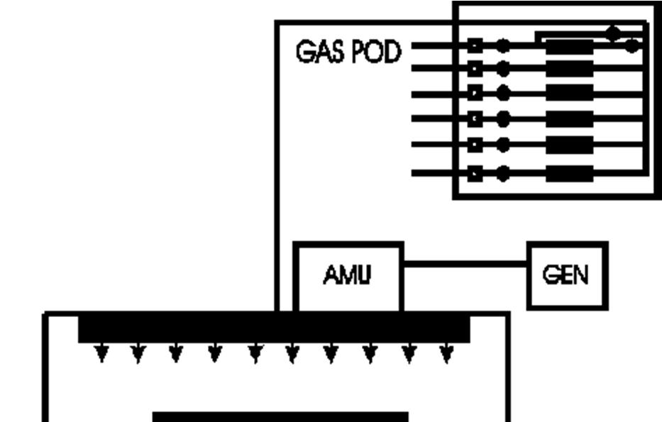
9 Carrier gas MOCVD (MOVPE) schematic Dopant 1 Filter & purifier MFC MFC MFC = mass flow controller controls the amount of gas going into the reactor Dopant 2 Group V precursor Carrier gas MFC MFC MFC MOVPE reactor Scrubber unit Gp. III precursor (in bubbler) Heater Power supply


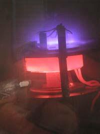
10 Example of a real GaN reactor
11 MOCVD Precursor purity Typical atomic density in a semiconductor: 5 x atoms cm -3 Typical doping density in semiconductor devices: cm -3 To avoid unintentional doping of devices, this implies a desired purity of better than 1 (10 14 /10 22 ) = %. Best available precursors are about % pure (referred to as 7 Nines or 7N), and are very expensive. Carbon contamination from metalorganic precursors may also be a source of unintentional doping, as may contaminated system components.
12 Monitoring MOCVD growth Typical in situ monitoring uses optical techniques Example: optical reflectivity measurements on GaN: laser beam transparent GaN epilayer Sapphire substrate Beams reflected from GaN surface and GaN/sapphire interface interfere. As film grows, nature of interference oscillates between constructive and destructive, resulting in oscillating intensity of reflected light This can be used to measure growth rate.
13 Comparison MOVPE Moderate pressure (100 mbar) Higher temperatures High throughput Hydrogen normally present Greater process drift Higher growth rates Highly toxic/explosive precursors Higher impurity levels $$$ MBE Ultra-low pressure (10-11 mbar) Lower temperatures Lower throughput No hydrogen unless deliberately added Precise thickness control Lower growth rates Safer precursors (usually!) Ultra-low impurity levels $$$$
14 Other Epitaxial Techniques Liquid Phase Epitaxy - Dipping or Tipping Chemical Beam Epitaxy - Combination of MBE and MOCVD

15 Laser Assisted Vapor Deposition He H 2 SiH 4, SF 6, H 2

16 Laser Assisted Catalytic growth Fig. 2 Schematic of a nanowire growth set up using a combination of laser ablation and vapor-liquid- solid scheme Fig.1 Semiconductor (GaAs) nanowires grown using laser assisted catalytic growth [1ref]. The scale bar corresponds to 50 nm.

17 PECVD (Plasma-Enhanced CVD)


18 Top-down versus bottom-up If we want to make a very small tree we can either Get a very big piece of wood and carve it into a much smaller model tree (TOP DOWN APPROACH) Plant a seed and then control its growth to form a fullyfunctioning bonsai tree (BOTTOM UP APPROACH)

19 Top-down approach: Nano and Micro Fabrication Techniques Ref. Ihn Chapter 6
20 Main fabrication processes Lithography Photolithography Electron beam lithography Scanning probe based lithography Etching: chemical wet etch, dry etching, laser ablation, focussed ion beam nanomachining, etc. Insulator deposition: PECVD, sputter-deposition Metal deposition: thermal evaporation (mostly e- beam evaporation)

21 Example of semiconductor device fabrication: p-n junction n - Si
22 Fabrication Steps for a p-n junction Oxidation or oxide deposition -Forming a SiO 2 layer. - Works as an insulator or barrier to diffusion or implantation Litographic Process - The wafer is covered by a photosensitive film; - Radiation Exposure through a mask; - The non-polymerized regions are solved; - Thermal Treatment ( ºC) to boost the film adhering; - Attack with HF to remove the uncovered SiO 2 ; - Photosensitive film removal through a chemical solution or through an attack of oxygen plasma. Jan 2006
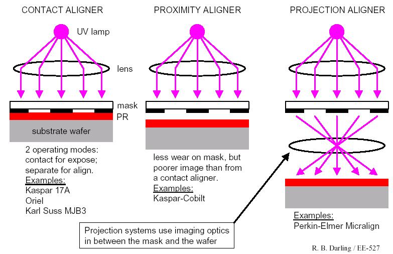
23 Photolithography The photolithography technique allows the manufacture of complex and dense circuits, improving this way the performance of the devices since it allows for its dimension reductions to happen. Recurring to the lithography technique, it s possible to manufacture on the same wafer both active and passive devices. The process consists in transferring a previously created pattern/model to the wafer s surface, in order to define the several regions of an integrated circuit This process has several steps, so all advances in the overall process depend on the development of each of the individual steps. Jan 2006
 Positive and Negative photoresists Masks Some issues edge bead Cleanliness is critical cleanroom")
24 Photolithography summary Surface Preparation Coating (Spin Casting) Pre-Bake (Soft Bake) Alignment Exposure Development Post-Bake (Hard Bake) Processing Using the Photoresist as a Mask Stripping Post Processing Cleaning (Ashing) Positive and Negative photoresists Masks Some issues edge bead Cleanliness is critical cleanroom

25 Birck Nanotechnology Center Nanofabrication Cleanroom 25,252 square feet Nanofabrication cleanroom coupled with a pharmaceutical grade cleanroom Material access between cleanrooms
 6 bays ISO Class 4 (Class 10) 5 bays ISO Class 5 (Class 100)")
26 Birck Nanotechnology Center Nanofabrication Cleanroom ISO Class 3 (Class 1) 6 bays ISO Class 4 (Class 10) 5 bays ISO Class 5 (Class 100) 2 bays
27 Photolithographic Process Steps The photolithography process must be implemented in a clean room, in order to avoid dust to be deposited in the mask and wafer. 1 - Deposition of the photosensitive film Spin Coating A drop of photosensitive material is placed on the center of the wafer. The wafer is then spinned over its axis in order to promote a uniform spreading of the material. Base Material : polyisopropene Conditions: rotation speed: rpm time: 10-60s thickness: m thermal treatment : 100ºC Jan 2006
28 2- Photosensitive film exposure to radiation The transfer of the model from the mask to the wafer can be done using optic equipment (for details bigger than 0.25 m), X-rays or by an electron beam. The photosensitive film when receiving radiation can behave as: - Positive photosensitive : The images formed are the same as the ones in the mask. - Negative photosensitive: The images formed are complementary to the ones in the mask. The radiation exposed regions become insoluble and therefore can not be removed. Jan 2006
29 Positive Photosensitive : It s built by 3 components: a resin, a photosensitive element and an organic solvent. The region exposed to radiation changes its chemical structure becoming soluble. The broken connections between the molecules allow an easy removal. Negative Photosensitive : Polymers are combined with a photosensitive element. The region exposed to radiation become insoluble due to the cross connections formed between the molecules. The high molecular weight of the molecules prevents their removal. Jan 2006
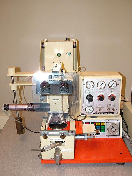
30 Tools for Photolithography
31 Exposure Response Curves and their transversal sections Photosensitive film fully soluble in developer for an energy equaling E T Photosensitive film fully insoluble for an energy equaling 2E T Jan 2006

32 3- Etching/Writing/Recording Process The next step is the etching process. That must allow the removal of material in the regions where the photosensitive film doesn t exist. SiO 2 is selectively attacked, whereas the substrate remains unaltered Jan 2006
. E.g.")
33 The simplest recording process is chemical recording: - It involves a chemical reaction followed by the removal of reaction elements. - The elements used for chemical attacks are mostly acids (HF, HNO 3, H 4 C 2 O 2, H 2 SO 4 ). E.g. : SiO 2 + 6HF -> H 2 SiF 6 + 2H 2 O Water can be used as diluent for this attacker Jan 2006

34 The Attack depends on the orientation degree: Some solutions are more easily solved in some specific crystallographic planes. The material used in the attack should attack only one layer at a time and should be self-limitative. Chemical recording is simple and cheap, however it s neither compatible with submicrometric technologies nor permits an anisotropic attack. Jan 2006
35 4 Photoresist Removal After the recording, the photosensitive film must be removed Usually, the film removal is made by chemical attack (acetone) Jan 2006
36 Manufacture Steps of a p-n junction Oxidation -Forming a SiO 2 layer. - Works as an insulator or barrier to diffusion or implantation Litographic Process - The wafer is covered by a photosensitive film; - Radiation Exposure through a mask; - The non-polymerized regions are solved; - Thermical Treatment ( ºC) to boost the film adhering; - Attack with HF to remove the uncovered SiO 2 ; - Photosensitive film removal through a chemical solution or through an attack of oxygen plasma. Jan 2006

37 In order to form active elements in integrated circuits it s necessary to selectively introduce dopants in the substrate; The surface is exposed to an high ion dopant concentration, that are incorporated in the semiconductor crystal lattice; The SiO 2 layer is a barrier to diffusion and to the impurity implantation. Jan 2006
38 Doping techniques: - Diffusion: Thermal Treatment in an oven at ºC on rich doping environment (e.g. Phosphorus or boron) - Ion Implantation : the doping atoms are ionized and accelerated against the surface in order to be implanted in the substrate Jan 2006

39 Metallization Ohmic Contact Formation, through a phased chemical or physical vapor deposition of a metallic film. A lithographic process is used in order to define contact zones. Metallization of the backside of the semiconductor. Thermal Treatment at ~500ºC in order to get low contact resistance between metallic layers and the semiconductor. Jan 2006
40 Other patterning techniques

41 J. Phys. Chem. B, Vol. 105, No. 24, 2001 Nanosphere Lithography


42 Two photon polymerization JOURNAL OF LIGHTWAVE TECHNOLOGY, VOL. 21, NO. 3, MARCH October 2004 / Vol. 12, No. 21 / OPTICS EXPRESS 5221


43 Interference Lithography Appl. Phys. Lett., Vol. 82, No. 8, 24 February 2003 H. Smith s group at MIT J. Appl. Phys., Vol. 82, No. 1, 1 July 1997
44 Plasmon based Phase mask Dip Pen Nano imprinting Soft Lithography Photonic alignment Other Techniques
Physics and Material Science of Semiconductor Nanostructures
 Physics and Material Science of Semiconductor Nanostructures PHYS 570P Prof. Oana Malis Email: omalis@purdue.edu Today Bulk semiconductor growth Single crystal techniques Nanostructure fabrication Epitaxial
Introduction to Photolithography
 http://www.ichaus.de/news/72 Introduction to Photolithography Photolithography The following slides present an outline of the process by which integrated circuits are made, of which photolithography is
Self-study problems and questions Processing and Device Technology, FFF110/FYSD13
 Self-study problems and questions Processing and Device Technology, FFF110/FYSD13 Version 2016_01 In addition to the problems discussed at the seminars and at the lectures, you can use this set of problems
Fabrication Technology, Part I
 EEL5225: Principles of MEMS Transducers (Fall 2004) Fabrication Technology, Part I Agenda: Microfabrication Overview Basic semiconductor devices Materials Key processes Oxidation Thin-film Deposition Reading:
Plasma Deposition (Overview) Lecture 1
 Lecture 1") Plasma Deposition (Overview) Lecture 1 Material Processes Plasma Processing Plasma-assisted Deposition Implantation Surface Modification Development of Plasma-based processing Microelectronics needs (fabrication
Plasma Deposition (Overview) Lecture 1 Material Processes Plasma Processing Plasma-assisted Deposition Implantation Surface Modification Development of Plasma-based processing Microelectronics needs (fabrication
CVD: General considerations.
 CVD: General considerations. PVD: Move material from bulk to thin film form. Limited primarily to metals or simple materials. Limited by thermal stability/vapor pressure considerations. Typically requires
4FNJDPOEVDUPS 'BCSJDBUJPO &UDI
 2010.5.4 1 Major Fabrication Steps in CMOS Process Flow UV light oxygen Silicon dioxide Silicon substrate Oxidation (Field oxide) photoresist Photoresist Coating Mask exposed photoresist Mask-Wafer Exposed
Thin Film Deposition
 Thin Film Deposition Physical processes Evaporation: Thermal, E-beam, Laser, Ion-plating. Sputtering: DC, RF, Magnetron, Reactive. Spray: Flame, Plasma. Chemical processes Chemical Vapor Deposition (CVD):
UNIT 3. By: Ajay Kumar Gautam Asst. Prof. Dev Bhoomi Institute of Technology & Engineering, Dehradun
 UNIT 3 By: Ajay Kumar Gautam Asst. Prof. Dev Bhoomi Institute of Technology & Engineering, Dehradun 1 Syllabus Lithography: photolithography and pattern transfer, Optical and non optical lithography, electron,
Lecture 150 Basic IC Processes (10/10/01) Page ECE Analog Integrated Circuits and Systems P.E. Allen
 Page ECE Analog Integrated Circuits and Systems P.E. Allen") Lecture 150 Basic IC Processes (10/10/01) Page 1501 LECTURE 150 BASIC IC PROCESSES (READING: TextSec. 2.2) INTRODUCTION Objective The objective of this presentation is: 1.) Introduce the fabrication of
Lecture 150 Basic IC Processes (10/10/01) Page 1501 LECTURE 150 BASIC IC PROCESSES (READING: TextSec. 2.2) INTRODUCTION Objective The objective of this presentation is: 1.) Introduce the fabrication of
Nanostructure. Materials Growth Characterization Fabrication. More see Waser, chapter 2
 Nanostructure Materials Growth Characterization Fabrication More see Waser, chapter 2 Materials growth - deposition deposition gas solid Physical Vapor Deposition Chemical Vapor Deposition Physical Vapor
TMT4320 Nanomaterials November 10 th, Thin films by physical/chemical methods (From chapter 24 and 25)
") 1 TMT4320 Nanomaterials November 10 th, 2015 Thin films by physical/chemical methods (From chapter 24 and 25) 2 Thin films by physical/chemical methods Vapor-phase growth (compared to liquid-phase growth)
1 TMT4320 Nanomaterials November 10 th, 2015 Thin films by physical/chemical methods (From chapter 24 and 25) 2 Thin films by physical/chemical methods Vapor-phase growth (compared to liquid-phase growth)
Film Deposition Part 1
 1 Film Deposition Part 1 Chapter 11 : Semiconductor Manufacturing Technology by M. Quirk & J. Serda Spring Semester 2013 Saroj Kumar Patra Semidonductor Manufacturing Technology, Norwegian University of
Lecture 0: Introduction
 Lecture 0: Introduction Introduction q Integrated circuits: many transistors on one chip q Very Large Scale Integration (VLSI): bucketloads! q Complementary Metal Oxide Semiconductor Fast, cheap, low power
Fabrication at the nanoscale for nanophotonics
 Fabrication at the nanoscale for nanophotonics Ilya Sychugov, KTH Materials Physics, Kista silicon nanocrystal by electron beam induced deposition lithography Outline of basic nanofabrication methods Devices
Wafer holders. Mo- or Ta- made holders Bonding: In (Ga), or In-free (clamped) Quick and easy transfer
, or In-free (clamped) Quick and easy transfer") Wafer holders Mo- or Ta- made holders Bonding: In (Ga), or In-free (clamped) Quick and easy transfer Image: In-free, 3-inch sample holder fitting a quarter of a 2- inch wafer Reflection High Energy Electron
Wafer holders Mo- or Ta- made holders Bonding: In (Ga), or In-free (clamped) Quick and easy transfer Image: In-free, 3-inch sample holder fitting a quarter of a 2- inch wafer Reflection High Energy Electron
Xing Sheng, 微纳光电子材料与器件工艺原理. Doping 掺杂. Xing Sheng 盛兴. Department of Electronic Engineering Tsinghua University
 微纳光电子材料与器件工艺原理 Doping 掺杂 Xing Sheng 盛兴 Department of Electronic Engineering Tsinghua University xingsheng@tsinghua.edu.cn 1 Semiconductor PN Junctions Xing Sheng, EE@Tsinghua LEDs lasers detectors solar
Lithography and Etching
 Lithography and Etching Victor Ovchinnikov Chapters 8.1, 8.4, 9, 11 Previous lecture Microdevices Main processes: Thin film deposition Patterning (lithography) Doping Materials: Single crystal (monocrystal)
Chapter 3 Engineering Science for Microsystems Design and Fabrication
 Lectures on MEMS and MICROSYSTEMS DESIGN and MANUFACTURE Chapter 3 Engineering Science for Microsystems Design and Fabrication In this Chapter, we will present overviews of the principles of physical and
Modern Methods in Heterogeneous Catalysis Research: Preparation of Model Systems by Physical Methods
 Modern Methods in Heterogeneous Catalysis Research: Preparation of Model Systems by Physical Methods Methods for catalyst preparation Methods discussed in this lecture Physical vapour deposition - PLD
Top down and bottom up fabrication
 Lecture 24 Top down and bottom up fabrication Lithography ( lithos stone / graphein to write) City of words lithograph h (Vito Acconci, 1999) 1930 s lithography press Photolithography d 2( NA) NA=numerical
UNIVERSITY OF CALIFORNIA College of Engineering Department of Electrical Engineering and Computer Sciences. Fall Exam 1
 UNIVERSITY OF CALIFORNIA College of Engineering Department of Electrical Engineering and Computer Sciences EECS 143 Fall 2008 Exam 1 Professor Ali Javey Answer Key Name: SID: 1337 Closed book. One sheet
ETCHING Chapter 10. Mask. Photoresist
 ETCHING Chapter 10 Mask Light Deposited Substrate Photoresist Etch mask deposition Photoresist application Exposure Development Etching Resist removal Etching of thin films and sometimes the silicon substrate
DEPOSITION OF THIN TiO 2 FILMS BY DC MAGNETRON SPUTTERING METHOD
 Chapter 4 DEPOSITION OF THIN TiO 2 FILMS BY DC MAGNETRON SPUTTERING METHOD 4.1 INTRODUCTION Sputter deposition process is another old technique being used in modern semiconductor industries. Sputtering
MEEN Nanoscale Issues in Manufacturing. Lithography Lecture 1: The Lithographic Process
 MEEN 489-500 Nanoscale Issues in Manufacturing Lithography Lecture 1: The Lithographic Process 1 Discuss Reading Assignment 1 1 Introducing Nano 2 2 Size Matters 3 3 Interlude One-The Fundamental Science
Semiconductor Technology
 Semiconductor Technology from A to Z Deposition www.halbleiter.org Contents Contents List of Figures II 1 Deposition 1 1.1 Plasma, the fourth aggregation state of a material............. 1 1.1.1 Plasma
CHAPTER 6: Etching. Chapter 6 1
 Chapter 6 1 CHAPTER 6: Etching Different etching processes are selected depending upon the particular material to be removed. As shown in Figure 6.1, wet chemical processes result in isotropic etching
Clean-Room microfabrication techniques. Francesco Rizzi Italian Institute of Technology
 Clean-Room microfabrication techniques Francesco Rizzi Italian Institute of Technology Miniaturization The first transistor Miniaturization The first transistor Miniaturization The first transistor Miniaturization
Techniken der Oberflächenphysik (Techniques of Surface Physics)
") Techniken der Oberflächenphysik (Techniques of Surface Physics) Prof. Yong Lei & Dr. Yang Xu (& Liying Liang) Fachgebiet 3D-Nanostrukturierung, Institut für Physik Contact: yong.lei@tu-ilmenau.de; yang.xu@tu-ilmenau.de;
Techniken der Oberflächenphysik (Techniques of Surface Physics) Prof. Yong Lei & Dr. Yang Xu (& Liying Liang) Fachgebiet 3D-Nanostrukturierung, Institut für Physik Contact: yong.lei@tu-ilmenau.de; yang.xu@tu-ilmenau.de;
Chemical Vapor Deposition *
 OpenStax-CNX module: m25495 1 Chemical Vapor Deposition * Andrew R. Barron This work is produced by OpenStax-CNX and licensed under the Creative Commons Attribution License 3.0 note: This module was developed
IC Fabrication Technology
 IC Fabrication Technology * History: 1958-59: J. Kilby, Texas Instruments and R. Noyce, Fairchild * Key Idea: batch fabrication of electronic circuits n entire circuit, say 10 7 transistors and 5 levels
Device Fabrication: Etch
 Device Fabrication: Etch 1 Objectives Upon finishing this course, you should able to: Familiar with etch terminology Compare wet and dry etch processes processing and list the main dry etch etchants Become
Secondary ion mass spectrometry (SIMS)
") Secondary ion mass spectrometry (SIMS) ELEC-L3211 Postgraduate Course in Micro and Nanosciences Department of Micro and Nanosciences Personal motivation and experience on SIMS Offers the possibility to
Secondary ion mass spectrometry (SIMS) ELEC-L3211 Postgraduate Course in Micro and Nanosciences Department of Micro and Nanosciences Personal motivation and experience on SIMS Offers the possibility to
Nanotechnology Fabrication Methods.
 Nanotechnology Fabrication Methods. 10 / 05 / 2016 1 Summary: 1.Introduction to Nanotechnology:...3 2.Nanotechnology Fabrication Methods:...5 2.1.Top-down Methods:...7 2.2.Bottom-up Methods:...16 3.Conclusions:...19
Ion Implant Part 1. Saroj Kumar Patra, TFE4180 Semiconductor Manufacturing Technology. Norwegian University of Science and Technology ( NTNU )
") 1 Ion Implant Part 1 Chapter 17: Semiconductor Manufacturing Technology by M. Quirk & J. Serda Spring Semester 2014 Saroj Kumar Patra,, Norwegian University of Science and Technology ( NTNU ) 2 Objectives
1 Ion Implant Part 1 Chapter 17: Semiconductor Manufacturing Technology by M. Quirk & J. Serda Spring Semester 2014 Saroj Kumar Patra,, Norwegian University of Science and Technology ( NTNU ) 2 Objectives
Etching Issues - Anisotropy. Dry Etching. Dry Etching Overview. Etching Issues - Selectivity
 Etching Issues - Anisotropy Dry Etching Dr. Bruce K. Gale Fundamentals of Micromachining BIOEN 6421 EL EN 5221 and 6221 ME EN 5960 and 6960 Isotropic etchants etch at the same rate in every direction mask
Lecture 6 Plasmas. Chapters 10 &16 Wolf and Tauber. ECE611 / CHE611 Electronic Materials Processing Fall John Labram 1/68
 Lecture 6 Plasmas Chapters 10 &16 Wolf and Tauber 1/68 Announcements Homework: Homework will be returned to you on Thursday (12 th October). Solutions will be also posted online on Thursday (12 th October)
Chapter 2 FABRICATION PROCEDURE AND TESTING SETUP. Our group has been working on the III-V epitaxy light emitting materials which could be
 Chapter 2 7 FABRICATION PROCEDURE AND TESTING SETUP 2.1 Introduction In this chapter, the fabrication procedures and the testing setups for the sub-micrometer lasers, the submicron disk laser and the photonic
Agenda. 1. Atomic Layer Deposition Technology
 Agenda 1. Atomic Layer Deposition Technology 2. What is ALD? Atomic Layer Deposition is invented in 1977 by T. Suntola et al. - New Deposition Method for Electro-Luminescent Display (ZnS:Mn Thin Films)
Photoresist Profile. Undercut: negative slope, common for negative resist; oxygen diffusion prohibits cross-linking; good for lift-off.
 Photoresist Profile 4-15 Undercut: negative slope, common for negative resist; oxygen diffusion prohibits cross-linking; good for lift-off undercut overcut Overcut: positive slope, common to positive resist,
EE C245 ME C218 Introduction to MEMS Design Fall 2007
 EE C245 ME C218 Introduction to MEMS Design Fall 2007 Prof. Clark T.-C. Nguyen Dept. of Electrical Engineering & Computer Sciences University of California at Berkeley Berkeley, CA 94720 Lecture 5: ALD,
Supplementary Figure 1 Detailed illustration on the fabrication process of templatestripped
 Supplementary Figure 1 Detailed illustration on the fabrication process of templatestripped gold substrate. (a) Spin coating of hydrogen silsesquioxane (HSQ) resist onto the silicon substrate with a thickness
Supplementary Information Our InGaN/GaN multiple quantum wells (MQWs) based one-dimensional (1D) grating structures
 based one-dimensional (1D) grating structures") Polarized white light from hybrid organic/iii-nitrides grating structures M. Athanasiou, R. M. Smith, S. Ghataora and T. Wang* Department of Electronic and Electrical Engineering, University of Sheffield,
Polarized white light from hybrid organic/iii-nitrides grating structures M. Athanasiou, R. M. Smith, S. Ghataora and T. Wang* Department of Electronic and Electrical Engineering, University of Sheffield,
EE-612: Lecture 22: CMOS Process Steps
 EE-612: Lecture 22: CMOS Process Steps Mark Lundstrom Electrical and Computer Engineering Purdue University West Lafayette, IN USA Fall 2006 NCN www.nanohub.org Lundstrom EE-612 F06 1 outline 1) Unit Process
Fabrication Technology for Miniaturization
 Appendix A Fabrication Technology for Miniaturization INTRODUCTION Many of the technologies that have enabled advances in miniaturization were first developed for microelectronics and allow both lateral
Atomic layer deposition of titanium nitride
 Atomic layer deposition of titanium nitride Jue Yue,version4, 04/26/2015 Introduction Titanium nitride is a hard and metallic material which has found many applications, e.g.as a wear resistant coating[1],
Halbleiter. Prof. Yong Lei. Prof. Thomas Hannappel.
 Halbleiter Prof. Yong Lei Prof. Thomas Hannappel yong.lei@tu-ilemnau.de thomas.hannappel@tu-ilmenau.de Important Events in Semiconductors History 1833 Michael Faraday discovered temperature-dependent conductivity
Photolithography 光刻 Part II: Photoresists
 微纳光电子材料与器件工艺原理 Photolithography 光刻 Part II: Photoresists Xing Sheng 盛兴 Department of Electronic Engineering Tsinghua University xingsheng@tsinghua.edu.cn 1 Photolithography 光刻胶 负胶 正胶 4 Photolithography
Hotwire-assisted Atomic Layer Deposition of Pure Metals and Metal Nitrides
 Hotwire-assisted Atomic Layer Deposition of Pure Metals and Metal Nitrides Alexey Kovalgin MESA+ Institute for Nanotechnology Semiconductor Components group a.y.kovalgin@utwente.nl 1 Motivation 1. Materials
CHAPTER 3: Epitaxy. City University of Hong Kong
 1 CHAPTER 3: Epitaxy Epitaxy (epi means "upon" and taxis means "ordered") is a term applied to processes used to grow a thin crystalline layer on a crystalline substrate. The seed crystal in epitaxial
Physics and Material Science of Semiconductor Nanostructures
 Physics and Material Science of Semiconductor Nanostructures PHYS 570P Prof. Oana Malis Email: omalis@purdue.edu Course website: http://www.physics.purdue.edu/academic_programs/courses/phys570p/ Lecture
Lecture 15 Etching. Chapters 15 & 16 Wolf and Tauber. ECE611 / CHE611 Electronic Materials Processing Fall John Labram 1/76
 Lecture 15 Etching Chapters 15 & 16 Wolf and Tauber 1/76 Announcements Term Paper: You are expected to produce a 4-5 page term paper on a selected topic (from a list). Term paper contributes 25% of course
Dry Etching Zheng Yang ERF 3017, MW 5:15-6:00 pm
 Dry Etching Zheng Yang ERF 3017, email: yangzhen@uic.edu, MW 5:15-6:00 pm Page 1 Page 2 Dry Etching Why dry etching? - WE is limited to pattern sizes above 3mm - WE is isotropic causing underetching -
A HYDROGEN SENSITIVE Pd/GaN SCHOTTKY DIODE SENSOR
 Journal of Physical Science, Vol. 17(2), 161 167, 2006 161 A HYDROGEN SENSITIVE Pd/GaN SCHOTTKY DIODE SENSOR A.Y. Hudeish 1,2* and A. Abdul Aziz 1 1 School of Physics, Universiti Sains Malaysia, 11800
Section 3: Etching. Jaeger Chapter 2 Reader
 Section 3: Etching Jaeger Chapter 2 Reader Etch rate Etch Process - Figures of Merit Etch rate uniformity Selectivity Anisotropy d m Bias and anisotropy etching mask h f substrate d f d m substrate d f
Preparation of Nanostructures(Příprava Nanostruktur)
") Preparation of Nanostructures (Příprava Nanostruktur) jaroslav.hamrle@vsb.cz September 23, 2013 Outline 1 Introduction 2 Bulk crystal growth 3 Thin film preparation 4 Lateral structures 5 Surface plasma
Preparation of Nanostructures (Příprava Nanostruktur) jaroslav.hamrle@vsb.cz September 23, 2013 Outline 1 Introduction 2 Bulk crystal growth 3 Thin film preparation 4 Lateral structures 5 Surface plasma
Kavli Workshop for Journalists. June 13th, CNF Cleanroom Activities
 Kavli Workshop for Journalists June 13th, 2007 CNF Cleanroom Activities Seeing nm-sized Objects with an SEM Lab experience: Scanning Electron Microscopy Equipment: Zeiss Supra 55VP Scanning electron microscopes
nmos IC Design Report Module: EEE 112
 nmos IC Design Report Author: 1302509 Zhao Ruimin Module: EEE 112 Lecturer: Date: Dr.Zhao Ce Zhou June/5/2015 Abstract This lab intended to train the experimental skills of the layout designing of the
Introduction. Photoresist : Type: Structure:
 Photoresist SEM images of the morphologies of meso structures and nanopatterns on (a) a positively nanopatterned silicon mold, and (b) a negatively nanopatterned silicon mold. Introduction Photoresist
OPTI510R: Photonics. Khanh Kieu College of Optical Sciences, University of Arizona Meinel building R.626
 OPTI510R: Photonics Khanh Kieu College of Optical Sciences, University of Arizona kkieu@optics.arizona.edu Meinel building R.626 Announcements HW#3 is assigned due Feb. 20 st Mid-term exam Feb 27, 2PM
Diffusion and Ion implantation Reference: Chapter 4 Jaeger or Chapter 3 Ruska N & P Dopants determine the resistivity of material Note N lower
 Diffusion and Ion implantation Reference: Chapter 4 Jaeger or Chapter 3 Ruska N & P Dopants determine the resistivity of material Note N lower resistavity than p: due to higher carrier mobility Near linear
High-density data storage: principle
 High-density data storage: principle Current approach High density 1 bit = many domains Information storage driven by domain wall shifts 1 bit = 1 magnetic nanoobject Single-domain needed Single easy axis
Semiconductor Physics and Devices
 Syllabus Advanced Nano Materials Semiconductor Physics and Devices Textbook Donald A. Neamen (McGraw-Hill) Semiconductor Physics and Devices Seong Jun Kang Department of Advanced Materials Engineering
LECTURE 5 SUMMARY OF KEY IDEAS
 LECTURE 5 SUMMARY OF KEY IDEAS Etching is a processing step following lithography: it transfers a circuit image from the photoresist to materials form which devices are made or to hard masking or sacrificial
Chapter 8 Ion Implantation
 Chapter 8 Ion Implantation 2006/5/23 1 Wafer Process Flow Materials IC Fab Metalization CMP Dielectric deposition Test Wafers Masks Thermal Processes Implant PR strip Etch PR strip Packaging Photolithography
2D MBE Activities in Sheffield. I. Farrer, J. Heffernan Electronic and Electrical Engineering The University of Sheffield
 2D MBE Activities in Sheffield I. Farrer, J. Heffernan Electronic and Electrical Engineering The University of Sheffield Outline Motivation Van der Waals crystals The Transition Metal Di-Chalcogenides
DQN Positive Photoresist
 UNIVESITY OF CALIFONIA, BEKELEY BEKELEY DAVIS IVINE LOS ANGELES IVESIDE SAN DIEGO SAN FANCISCO SANTA BABAA SANTA CUZ DEPATMENT OF BIOENGINEEING 94720-1762 BioE 121 Midterm #1 Solutions BEKELEY, CALIFONIA
Ion Implantation. alternative to diffusion for the introduction of dopants essentially a physical process, rather than chemical advantages:
 Ion Implantation alternative to diffusion for the introduction of dopants essentially a physical process, rather than chemical advantages: mass separation allows wide varies of dopants dose control: diffusion
Etching: Basic Terminology
 Lecture 7 Etching Etching: Basic Terminology Introduction : Etching of thin films and sometimes the silicon substrate are very common process steps. Usually selectivity, and directionality are the first
MSN551 LITHOGRAPHY II
 MSN551 Introduction to Micro and Nano Fabrication LITHOGRAPHY II E-Beam, Focused Ion Beam and Soft Lithography Why need electron beam lithography? Smaller features are required By electronics industry:
Wet and Dry Etching. Theory
 Wet and Dry Etching Theory 1. Introduction Etching techniques are commonly used in the fabrication processes of semiconductor devices to remove selected layers for the purposes of pattern transfer, wafer
Nanostructures Fabrication Methods
 Nanostructures Fabrication Methods bottom-up methods ( atom by atom ) In the bottom-up approach, atoms, molecules and even nanoparticles themselves can be used as the building blocks for the creation of
EE 527 MICROFABRICATION. Lecture 24 Tai-Chang Chen University of Washington
 EE 527 MICROFABRICATION Lecture 24 Tai-Chang Chen University of Washington EDP ETCHING OF SILICON - 1 Ethylene Diamine Pyrocatechol Anisotropy: (100):(111) ~ 35:1 EDP is very corrosive, very carcinogenic,
EV Group. Engineered Substrates for future compound semiconductor devices
 EV Group Engineered Substrates for future compound semiconductor devices Engineered Substrates HB-LED: Engineered growth substrates GaN / GaP layer transfer Mobility enhancement solutions: III-Vs to silicon
Pattern Transfer- photolithography
 Pattern Transfer- photolithography DUV : EUV : 13 nm 248 (KrF), 193 (ArF), 157 (F 2 )nm H line: 400 nm I line: 365 nm G line: 436 nm Wavelength (nm) High pressure Hg arc lamp emission Ref: Campbell: 7
EE130: Integrated Circuit Devices
 EE130: Integrated Circuit Devices (online at http://webcast.berkeley.edu) Instructor: Prof. Tsu-Jae King (tking@eecs.berkeley.edu) TA s: Marie Eyoum (meyoum@eecs.berkeley.edu) Alvaro Padilla (apadilla@eecs.berkeley.edu)
Photolithography Overview 9/29/03 Brainerd/photoclass/ECE580/Overvie w/overview
 http://www.intel.com/research/silicon/mooreslaw.htm 1 Moore s law only holds due to photolithography advancements in reducing linewidths 2 All processing to create electric components and circuits rely
EE C245 ME C218 Introduction to MEMS Design Fall 2007
 EE C245 ME C218 Introduction to MEMS Design Fall 2007 Prof. Clark T.-C. Nguyen Dept. of Electrical Engineering & Computer Sciences University of California at Berkeley Berkeley, CA 94720 Lecture 4: Film
UNIVERSITY OF CALIFORNIA College of Engineering Department of Electrical Engineering and Computer Sciences. Professor Ali Javey. Fall 2009.
 UNIVERSITY OF CALIFORNIA College of Engineering Department of Electrical Engineering and Computer Sciences EE143 Professor Ali Javey Fall 2009 Exam 1 Name: SID: Closed book. One sheet of notes is allowed.
UNIVERSITY OF CALIFORNIA College of Engineering Department of Electrical Engineering and Computer Sciences. Professor Ali Javey. Spring 2009.
 UNIVERSITY OF CALIFORNIA College of Engineering Department of Electrical Engineering and Computer Sciences EE143 Professor Ali Javey Spring 2009 Exam 1 Name: SID: Closed book. One sheet of notes is allowed.
E SC 412 Nanotechnology: Materials, Infrastructure, and Safety Wook Jun Nam
 E SC 412 Nanotechnology: Materials, Infrastructure, and Safety Wook Jun Nam Lecture 10 Outline 1. Wet Etching/Vapor Phase Etching 2. Dry Etching DC/RF Plasma Plasma Reactors Materials/Gases Etching Parameters
PREPARATION OF LUMINESCENT SILICON NANOPARTICLES BY PHOTOTHERMAL AEROSOL SYNTHESIS FOLLOWED BY ACID ETCHING
 Phase Transitions Vol. 77, Nos. 1 2, January February 2004, pp. 131 137 PREPARATION OF LUMINESCENT SILICON NANOPARTICLES BY PHOTOTHERMAL AEROSOL SYNTHESIS FOLLOWED BY ACID ETCHING X. LI, Y. HE, S.S. TALUKDAR
Chapter 7 Plasma Basic
 Chapter 7 Plasma Basic Hong Xiao, Ph. D. hxiao89@hotmail.com www2.austin.cc.tx.us/hongxiao/book.htm Hong Xiao, Ph. D. www2.austin.cc.tx.us/hongxiao/book.htm 1 Objectives List at least three IC processes
JOHN G. EKERDT RESEARCH FOCUS
 JOHN G. EKERDT RESEARCH FOCUS We study the surface, growth and materials chemistry of metal, dielectric, ferroelectric, and polymer thin films. We seek to understand and describe nucleation and growth
Structuring and bonding of glass-wafers. Dr. Anke Sanz-Velasco
 Structuring and bonding of glass-wafers Dr. Anke Sanz-Velasco Outline IMT Why glass? Components for life science Good bond requirements and evaluation Wafer bonding 1. Fusion bonding 2. UV-adhesive bonding
A Novel Approach to the Layer Number-Controlled and Grain Size- Controlled Growth of High Quality Graphene for Nanoelectronics
 Supporting Information A Novel Approach to the Layer Number-Controlled and Grain Size- Controlled Growth of High Quality Graphene for Nanoelectronics Tej B. Limbu 1,2, Jean C. Hernández 3, Frank Mendoza
ESH Benign Processes for he Integration of Quantum Dots (QDs)
") ESH Benign Processes for he Integration of Quantum Dots (QDs) PIs: Karen K. Gleason, Department of Chemical Engineering, MIT Graduate Students: Chia-Hua Lee: PhD Candidate, Department of Material Science
ESH Benign Processes for he Integration of Quantum Dots (QDs) PIs: Karen K. Gleason, Department of Chemical Engineering, MIT Graduate Students: Chia-Hua Lee: PhD Candidate, Department of Material Science
Lecture 11. Etching Techniques Reading: Chapter 11. ECE Dr. Alan Doolittle
 Lecture 11 Etching Techniques Reading: Chapter 11 Etching Techniques Characterized by: 1.) Etch rate (A/minute) 2.) Selectivity: S=etch rate material 1 / etch rate material 2 is said to have a selectivity
3.155J/6.152J Microelectronic Processing Technology Fall Term, 2004
 3.155J/6.152J Microelectronic Processing Technology Fall Term, 2004 Bob O'Handley Martin Schmidt Quiz Nov. 17, 2004 Ion implantation, diffusion [15] 1. a) Two identical p-type Si wafers (N a = 10 17 cm
Advanced Texturing of Si Nanostructures on Low Lifetime Si Wafer
 Advanced Texturing of Si Nanostructures on Low Lifetime Si Wafer SUHAILA SEPEAI, A.W.AZHARI, SALEEM H.ZAIDI, K.SOPIAN Solar Energy Research Institute (SERI), Universiti Kebangsaan Malaysia (UKM), 43600
5. Photochemistry of polymers
 5. Photochemistry of polymers 5.1 Photopolymerization and cross-linking Photopolymerization The fundamental principle of photopolymerization is based on the photoinduced production of a reactive species,
Three Approaches for Nanopatterning
 Three Approaches for Nanopatterning Lithography allows the design of arbitrary pattern geometry but maybe high cost and low throughput Self-Assembly offers high throughput and low cost but limited selections
Chapter 3 Basics Semiconductor Devices and Processing
 Chapter 3 Basics Semiconductor Devices and Processing Hong Xiao, Ph. D. www2.austin.cc.tx.us/hongxiao/book.htm Hong Xiao, Ph. D. www2.austin.cc.tx.us/hongxiao/book.htm 1 Objectives Identify at least two
RESEARCH ON BENZENE VAPOR DETECTION USING POROUS SILICON
 Section Micro and Nano Technologies RESEARCH ON BENZENE VAPOR DETECTION USING POROUS SILICON Assoc. Prof. Ersin Kayahan 1,2,3 1 Kocaeli University, Electro-optic and Sys. Eng. Umuttepe, 41380, Kocaeli-Turkey
T: +44 (0) W:
 W:") Ultraviolet Deposition of Thin Films and Nanostructures Ian W. Boyd ETC Brunel University Kingston Lane Uxbridge Middx UB8 3PH UK T: +44 (0)1895 267419 W: etcbrunel.co.uk E: ian.boyd@brunel.ac.uk Outline
Ultraviolet Deposition of Thin Films and Nanostructures Ian W. Boyd ETC Brunel University Kingston Lane Uxbridge Middx UB8 3PH UK T: +44 (0)1895 267419 W: etcbrunel.co.uk E: ian.boyd@brunel.ac.uk Outline
Semiconductor Device Physics
 1 Semiconductor Device Physics Lecture 1 http://zitompul.wordpress.com 2 0 1 3 2 Semiconductor Device Physics Textbook: Semiconductor Device Fundamentals, Robert F. Pierret, International Edition, Addison
Semiconductors Reference: Chapter 4 Jaeger or Chapter 3 Ruska Recall what determines conductor, insulator and semiconductor Plot the electron energy
 Semiconductors Reference: Chapter 4 Jaeger or Chapter 3 Ruska Recall what determines conductor, insulator and semiconductor Plot the electron energy states of a material In some materials get the creation
Lecture 1. Introduction to Electronic Materials. Reading: Pierret 1.1, 1.2, 1.4,
 Lecture 1 Introduction to Electronic Materials Reading: Pierret 1.1, 1.2, 1.4, 2.1-2.6 Atoms to Operational Amplifiers The goal of this course is to teach the fundamentals of non-linear circuit elements
Ajay Kumar Gautam Asst. Prof. Electronics & Communication Engineering Dev Bhoomi Institute of Technology & Engineering Dehradun UNIT II
 Ajay Kumar Gautam Asst. Prof. Electronics & Communication Engineering Dev Bhoomi Institute of Technology & Engineering Dehradun UNIT II Syllabus EPITAXIAL PROCESS: Epitaxy and its concept, Growth kinetics
SUPPLEMENTARY NOTES Supplementary Note 1: Fabrication of Scanning Thermal Microscopy Probes
 SUPPLEMENTARY NOTES Supplementary Note 1: Fabrication of Scanning Thermal Microscopy Probes Fabrication of the scanning thermal microscopy (SThM) probes is summarized in Supplementary Fig. 1 and proceeds