Ion beam lithography
|
|
|
- Chester Scott
- 5 years ago
- Views:
Transcription
1 Ion beam lithography Progress in ion technology spot size <10nm Direct writing : resist, milling, implantation Ions rapidely absorbed by matter almost no proximity effect low dose - 3D structures possibles
2 Ions trajectories
 Energy dispersion")


3 Liquid Metal Ion Source (LMIS) Energy dispersion : 4eV Spot size limited by chromatic aberratrions : 3nm Brgihtness 10 6 A/cm 2.sr Good current stability


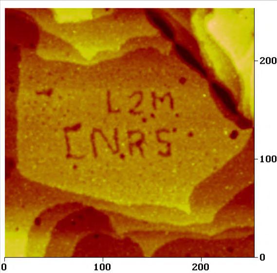
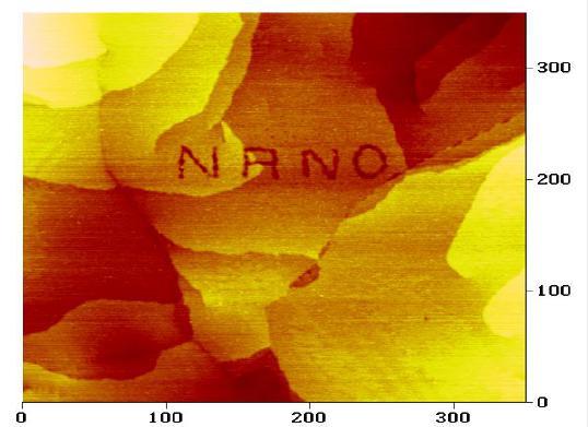
4 examples 30kV ions Gallium Hole in a Si 3 N 4 membrane 10 nm LPN Marcoussis

5 3nm hole pierced in a 20nm thick SiC membrane 3 nm LPN Marcoussis

6 Inorganic resist AlF3 LPN Marcoussis

 Pt (4,5 nm)")


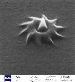
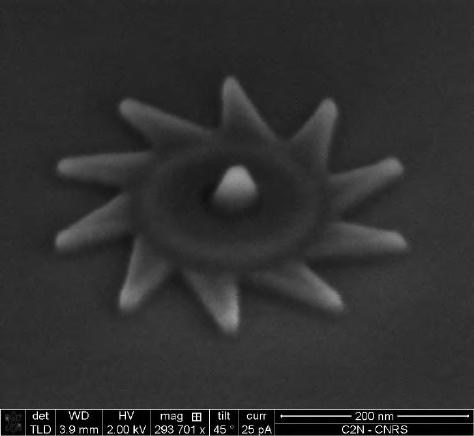
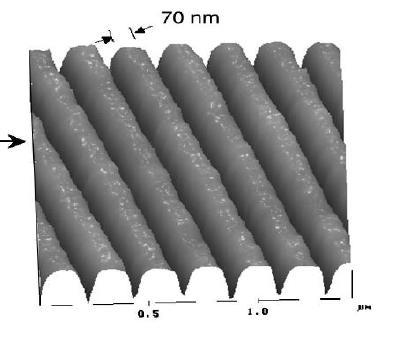
7 Magnetic field patterning FIB probe Pattern Pt (3,4 nm) Co (1,4 nm) Pt (4,5 nm) Transparent alumina substrate Kerr image of the patterned PtCoPt film (Ga + ions, 30 kev, ions/cm 2 ). define stable domains: 1500 nm, 750 nm, 300 nm, 50 nm
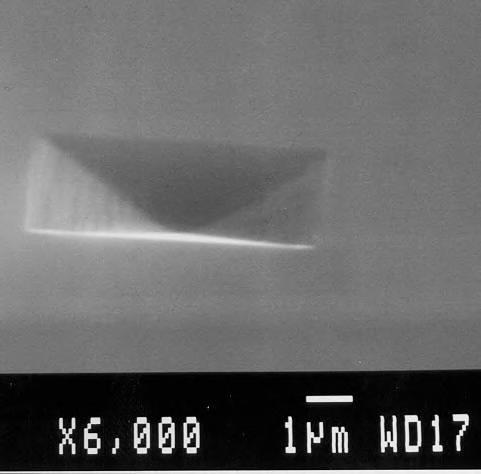
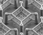
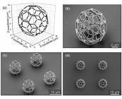
8 3D shape


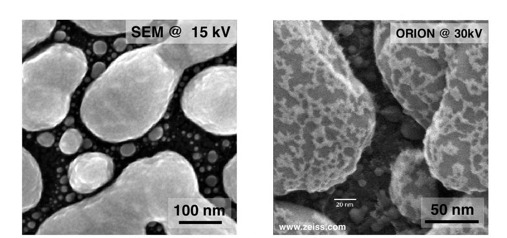
9 Helium microscope T=75K A trimer of W atoms emits the He ions: spot on the sample ~0.3-0,5nm Plasma cleaning 9

10 An atomic size source Source is one atome spot size can be as low as 0.35nm on sample

11 Small spatial extension of the diffused He ions SEM images are produced by SE1 and SE2 electron Here it is mostly SE1 small sppatial extension and sensitivity to surface


12 12 Overall equipment Plasma cleaner Electron detector


 high precision, no interdiffusion (Ga ions).")

13 13 A versatile tool Microscope : high resolution, sensitive to surface, very high deep of focus, flood to neutralize ions allows imaging insulator and biological stuff Lithography : high sensitivity, high resolution, no proximity effect. microscopy lithography Direct milling : low damage ( low sputter yield) high precision, no interdiffusion (Ga ions). Possibility to use Neon for higher yield but less stability and resolution milling Beam induced deposition : W, Pt,SiO 2 no contamination deposition

14 June 2018 A microscope
15

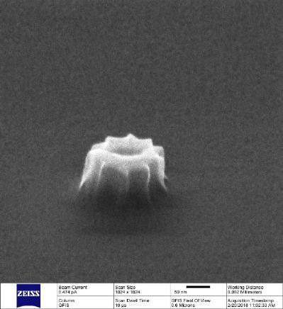
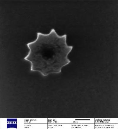
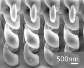
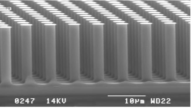
16 June 2018 High resolution lithography with HSQ Sub 10nm achieved


17 nanolithography Development on a new resist based on Aluminum oxide. Better resist profile and roughness than HSQ Width below 10nm can be easily achieved with an aspect ration higher than 4. C2N C2N Dense lines C2N C2N


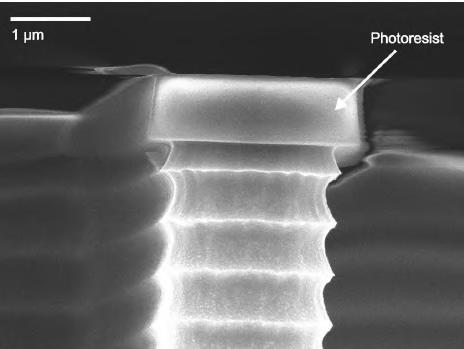
18 RIE etching of Silicon with the AlOx resist Good selectivity with fluorine based etching. We obtain 5nm width and 40nm height Silicone nanowires.


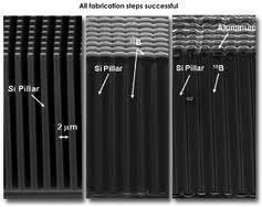
19 7-8 Project 19 June Meeting 2018 Graz AlOx resist 80nm 400 nm

20 7-8 Project 20 June Meeting 2018 Graz


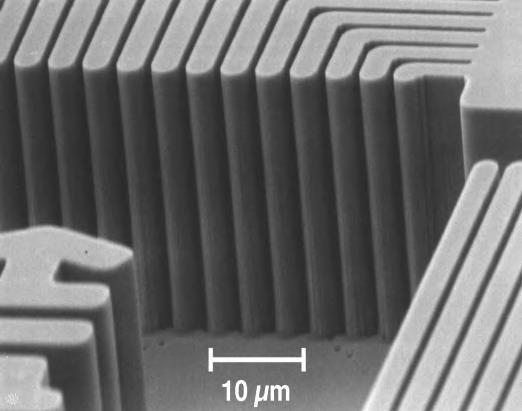
21 High precision milling C2N C2N Hole in suspended graphene : dia<5nm Nanogap etched on a gold bridge for molecule grafting (collab C2N, ICMMO)

22 June 2018 etching
 3 For cooper : Cu(C 5 HF 6 O 2 ) 2 usually C")
23 Beam induced deposition Precursors mostly metal carbonyls: Me(CO)x W(CO) 6, Fe(CO) 5 For platinium :C 5 H 4 CH 3 Pt(CH 3 ) 3 For cooper : Cu(C 5 HF 6 O 2 ) 2 usually C contimination


24 24 Growing W wire ( in fact W 0.7 C 0.3 )

25 June 2018


26 Commercial equipment Source Gallium 30kV 750k Source Hélium or Néon 30kV 1.2M

27 The dual beams Electron column: insitu real time Observation Ion column : milling, cutting and beam induced deposition.
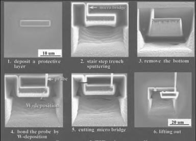
28 TEM preparation
29 Near field lithography

30 Near field methodology Electric pulse Mechanical pressure Under threshold threshold Alignment, observation
31 More pratical : local anodization Water condensed b) Monolayer of gold oxyde H 2 O atomic flat gold oxygen gold c) Exchage process d) Dissoution of gold atom

32 exemples Z.Z. Wang LPN


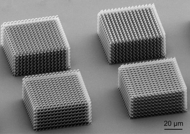
33 Other examples Anodisa²on of GaAs Anodisation du Nb Aharonov-Bohm ring ETH Zürich SQUID CRTBT

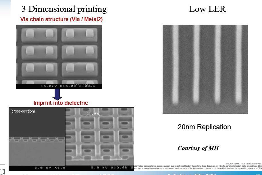
34 Engraving resist with an AFM tip Single electron transistor made by AFM litho PhD thesis V. Bouchiat

35 Nano-imprint 1.temp +pressure 50Bars mold substrate 2. cooling 3. dimolding (ca be tricky) 4. Residus etchnig Slow process, mask 1/1 scale i.e. ebeam lithography 10nm resolution demonstrated, very cheap
36 examples
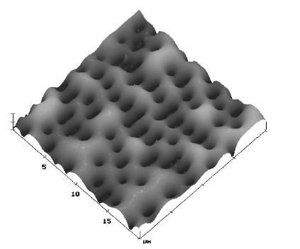
37 UV assisted imprint Quartz mold substrate Resist hardening underuv Faster
38 resolution
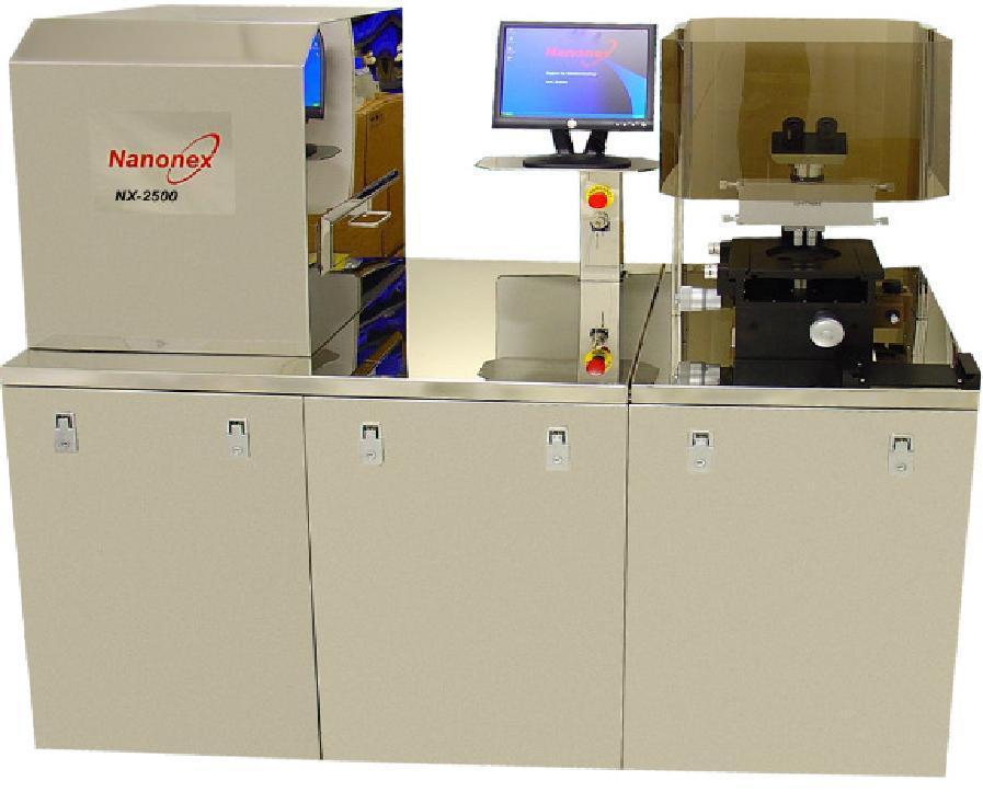
39 Commercial equipment
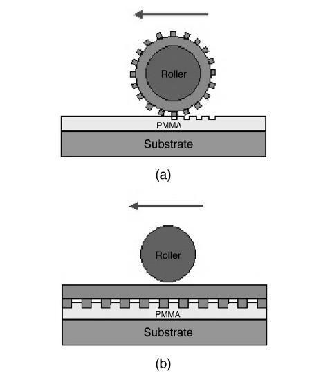
40 Roller lithography Easy and rapid but simple pattern solar cells?

41 Soft lithography PDMS mold
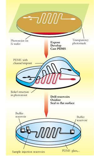
42 microfluidics

 PDMS A:B 1:20 1:5 PDMS")
43 M.A. Unger, H-P Chou, T. Thorsen, A. Scherer, and S.R. Quake, Science 288, p.113 (2000) PDMS A:B 1:20 1:5 PDMS bi-couche Fluidigm (USA)

44 Litho 3D laser The wavelength of the LASER ido not produce any change in the resist But at the focal point where the intensity is very strong -> Two photons process -> resist polymerisation The sample is scanned under the focal point
45 Resolution 200nm à 300nm
46 Conclusions on lithography Technique Resolution Use Remarks contact 0.25 m Labs et R&D Cheap intermediate resolution Optical lithograpphy proximity 2 m Labs and R&D Cheap but low resolution projection 20nm Industry Very expensive EUV <10nm? Industry Need some work 2020? Ebeam lithography 1nm Labs et R&D Mask making Easy to handle no mask very high resolution Intermediate cost Ion beam lithography 1nm Labs et R&D Milling and lithography diagnostic Near field lithography Atom 10nm Labs Very slow, cheap for specific appl. Nano-imprint 10nm Labs and industry? Cheap, alignment issu specific
47 Transfert techniques Wet etchnig Ion etching Reactive ion beam etchnig

48 Wet etchnig Isotrope etching (non crystallin materials) Simple Fast Pb of undercut Difficult to control : if weak chemistry long time but surface state important
49 Anisotropic wet etching (crystalline material)
50 MEMS suspended structures
51
52 Ion Beam Etching (IBE) Mechanical impact of the ions Etchnig rate T gase anode Ar Ar + e accelerated Ions T E ZU U Binding energy Z atomic number E ion energy x coeff (angle) Typical energy: 100eV to 2kV Collimation grids
53 Poor etching rate Not very anisotrope Not very selective Re-deposition Trenching Defect Ion beam etching
54 Reactive ion etching: RIE rf C plasma
55 plasma Plasma = partially ionized gase with ions (+or -) électrons and neutral species Create by radiofrequency or microwave discharge at gase pressure typically 100Pa ( 1Torr) Although the gase is at ambient temperature, the electron energy create very active ions radicals usually obtained at high temperature Chemical reactivity of the surface is also modified by the impact of the ions. The interplay between chemical and physical effect give rise to very anisotropic and high rate etching. Plasmas are quite complex systems and it is difficult to master all the parameters.
56 Autopolarisation Speed of electron >> speed of ion because of mass difference During an RF cycle all electrons reach the electrode but not all the ions DC polarisation lock by the capacity The ions are accelerated by this voltage to the sample Zone neutre
57 Autopolarisation At the first positive voltage an important flux of electrons arrive on the electrode but at the next negative one a much smaller number of ions arrive. A negative voltage built up and repell the electrons. The stationary state arise when the flux of electrons = flux of ions. Mean potential The plasma is at a positive potential since the electron are rapidely evacuated by the chamber wall. Vp allows to maintained the neutral charge of the plasma, This the most positive charge of the system.


58 autopolarisation The polarisation depends on the ratio between the two electrodes. The mass electrode include the wall of the reactor and Vdc >> Vp sample The pollution of the reactor change the area of the mass electrode and the polarisation evolve with time
59 chemistry non active specie Active species created diffusion diffusion adsorption reaction desorption
60 Chemical aspects Example: CF4 is not active on Si but F is active The desorption process of the chemical reaction is important otherwise the surface is passivated. Ex : Al react with F AlF3 but vapor pressure AlF3 1 torr even at 1000 C Si + F SiF non volatile SiF + F SiF2 non volatile SiF2 + F SiF3 non volatile SiF3 + F SiF4 volatile The chemical reaction are activated by electrons and ions bombardment creating active sites.
61 Chemical+physical Pure chemical Pure physical
62 Anisotropy Active element Passivation gase masque Active element stop by passivation The edge which are less bombarded are protected

63 Bosch MEMS application (Collège de France-LPN-ESIEE)

64 RIE Pros Easy to handle High rate Selectivity Anisotropy No redeposition RIE Cons Sensitive to pollution drift in etch rate Plasma density quite small cm -3 Energy and pressure are linked difficult to separate physic to chemistry


65 Examples RIE 1,94µm x 6,25µm AlAs/GaAs micropillar 7.5 µm depth 1.2mm diameter0.4mm


66 Reactive Ion Beam Ething:RIBE gas O O e Idem IBE but with chemical ions instead of Argon Complete separation between energy and chemistry Give impressive aspect ratio Quite high voltage defects Needs plasma electron source (filament burn)

67 Example RIBE
68 Electron Cyclotron Resonance Very dense plasma (high rate) at low energy (less defects) Independent control energy/density of ions fecr=2.4ghz Adjust plasma density ECR : cyclotron 2π f = eb/m in phase with Microwave field B E wt=0 B E wt=p/4 B E wt=p/2 Adjust ions energy B E wt=3p/4 There is a space slab where cyclotron and microwave are in phase Plasma density cm -3

69 Example ECR etching
70 ICP : inductively Coupled Plasma The plasma is create by a oscillating magnetic field The oscillating magnetic field create an electric field :cf Maxwell The plasma is better confined than with condensator plate rote = B t A voltage applied on the substrate holder allows to control the energy of the impining ions density10 12 cm -3
Etching Issues - Anisotropy. Dry Etching. Dry Etching Overview. Etching Issues - Selectivity
 Etching Issues - Anisotropy Dry Etching Dr. Bruce K. Gale Fundamentals of Micromachining BIOEN 6421 EL EN 5221 and 6221 ME EN 5960 and 6960 Isotropic etchants etch at the same rate in every direction mask
Nova 600 NanoLab Dual beam Focused Ion Beam IITKanpur
 Nova 600 NanoLab Dual beam Focused Ion Beam system @ IITKanpur Dual Beam Nova 600 Nano Lab From FEI company (Dual Beam = SEM + FIB) SEM: The Electron Beam for SEM Field Emission Electron Gun Energy : 500
ETCHING Chapter 10. Mask. Photoresist
 ETCHING Chapter 10 Mask Light Deposited Substrate Photoresist Etch mask deposition Photoresist application Exposure Development Etching Resist removal Etching of thin films and sometimes the silicon substrate
Reactive Ion Etching (RIE)
") Reactive Ion Etching (RIE) RF 13.56 ~ MHz plasma Parallel-Plate Reactor wafers Sputtering Plasma generates (1) Ions (2) Activated neutrals Enhance chemical reaction 1 2 Remote Plasma Reactors Plasma Sources
Reactive Ion Etching (RIE) RF 13.56 ~ MHz plasma Parallel-Plate Reactor wafers Sputtering Plasma generates (1) Ions (2) Activated neutrals Enhance chemical reaction 1 2 Remote Plasma Reactors Plasma Sources
Etching: Basic Terminology
 Lecture 7 Etching Etching: Basic Terminology Introduction : Etching of thin films and sometimes the silicon substrate are very common process steps. Usually selectivity, and directionality are the first
Nanofabrication Techniques. Dominique Mailly Laboratoire de Photonique et de Nanostructures Marcoussis
 Nanofabrication Techniques Dominique Mailly Laboratoire de Photonique et de Nanostructures Marcoussis Summary Introduction Optical Lithography X-ray lithography E-beam Lithography Ion beam Lithography
Section 3: Etching. Jaeger Chapter 2 Reader
 Section 3: Etching Jaeger Chapter 2 Reader Etch rate Etch Process - Figures of Merit Etch rate uniformity Selectivity Anisotropy d m Bias and anisotropy etching mask h f substrate d f d m substrate d f
EE 527 MICROFABRICATION. Lecture 24 Tai-Chang Chen University of Washington
 EE 527 MICROFABRICATION Lecture 24 Tai-Chang Chen University of Washington EDP ETCHING OF SILICON - 1 Ethylene Diamine Pyrocatechol Anisotropy: (100):(111) ~ 35:1 EDP is very corrosive, very carcinogenic,
UNIT 3. By: Ajay Kumar Gautam Asst. Prof. Dev Bhoomi Institute of Technology & Engineering, Dehradun
 UNIT 3 By: Ajay Kumar Gautam Asst. Prof. Dev Bhoomi Institute of Technology & Engineering, Dehradun 1 Syllabus Lithography: photolithography and pattern transfer, Optical and non optical lithography, electron,
MSN551 LITHOGRAPHY II
 MSN551 Introduction to Micro and Nano Fabrication LITHOGRAPHY II E-Beam, Focused Ion Beam and Soft Lithography Why need electron beam lithography? Smaller features are required By electronics industry:
E SC 412 Nanotechnology: Materials, Infrastructure, and Safety Wook Jun Nam
 E SC 412 Nanotechnology: Materials, Infrastructure, and Safety Wook Jun Nam Lecture 10 Outline 1. Wet Etching/Vapor Phase Etching 2. Dry Etching DC/RF Plasma Plasma Reactors Materials/Gases Etching Parameters
Lecture 6 Plasmas. Chapters 10 &16 Wolf and Tauber. ECE611 / CHE611 Electronic Materials Processing Fall John Labram 1/68
 Lecture 6 Plasmas Chapters 10 &16 Wolf and Tauber 1/68 Announcements Homework: Homework will be returned to you on Thursday (12 th October). Solutions will be also posted online on Thursday (12 th October)
CHAPTER 6: Etching. Chapter 6 1
 Chapter 6 1 CHAPTER 6: Etching Different etching processes are selected depending upon the particular material to be removed. As shown in Figure 6.1, wet chemical processes result in isotropic etching
Plasma etching. Bibliography
 Plasma etching Bibliography 1. B. Chapman, Glow discharge processes, (Wiley, New York, 1980). - Classical plasma processing of etching and sputtering 2. D. M. Manos and D. L. Flamm, Plasma etching; An
Wet and Dry Etching. Theory
 Wet and Dry Etching Theory 1. Introduction Etching techniques are commonly used in the fabrication processes of semiconductor devices to remove selected layers for the purposes of pattern transfer, wafer
LECTURE 5 SUMMARY OF KEY IDEAS
 LECTURE 5 SUMMARY OF KEY IDEAS Etching is a processing step following lithography: it transfers a circuit image from the photoresist to materials form which devices are made or to hard masking or sacrificial
Supplementary Figure 1 Detailed illustration on the fabrication process of templatestripped
 Supplementary Figure 1 Detailed illustration on the fabrication process of templatestripped gold substrate. (a) Spin coating of hydrogen silsesquioxane (HSQ) resist onto the silicon substrate with a thickness
TMT4320 Nanomaterials November 10 th, Thin films by physical/chemical methods (From chapter 24 and 25)
") 1 TMT4320 Nanomaterials November 10 th, 2015 Thin films by physical/chemical methods (From chapter 24 and 25) 2 Thin films by physical/chemical methods Vapor-phase growth (compared to liquid-phase growth)
1 TMT4320 Nanomaterials November 10 th, 2015 Thin films by physical/chemical methods (From chapter 24 and 25) 2 Thin films by physical/chemical methods Vapor-phase growth (compared to liquid-phase growth)
Etching Capabilities at Harvard CNS. March 2008
 Etching Capabilities at Harvard CNS March 2008 CNS: A shared use facility for the Harvard Community and New England CNS Provides technical support, equipment and staff. Explicitly multi-disciplinary w/
EE 527 MICROFABRICATION. Lecture 25 Tai-Chang Chen University of Washington
 EE 527 MICROFABRICATION Lecture 25 Tai-Chang Chen University of Washington ION MILLING SYSTEM Kaufmann source Use e-beam to strike plasma A magnetic field applied to increase ion density Drawback Low etch
Lecture 11. Etching Techniques Reading: Chapter 11. ECE Dr. Alan Doolittle
 Lecture 11 Etching Techniques Reading: Chapter 11 Etching Techniques Characterized by: 1.) Etch rate (A/minute) 2.) Selectivity: S=etch rate material 1 / etch rate material 2 is said to have a selectivity
Chapter 7 Plasma Basic
 Chapter 7 Plasma Basic Hong Xiao, Ph. D. hxiao89@hotmail.com www2.austin.cc.tx.us/hongxiao/book.htm Hong Xiao, Ph. D. www2.austin.cc.tx.us/hongxiao/book.htm 1 Objectives List at least three IC processes
Regents of the University of California
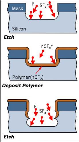
 Deep Reactive-Ion Etching (DRIE) DRIE Issues: Etch Rate Variance The Bosch process: Inductively-coupled plasma Etch Rate: 1.5-4 μm/min Two main cycles in the etch: Etch cycle (5-15 s): SF 6 (SF x+ ) etches
Fabrication at the nanoscale for nanophotonics
 Fabrication at the nanoscale for nanophotonics Ilya Sychugov, KTH Materials Physics, Kista silicon nanocrystal by electron beam induced deposition lithography Outline of basic nanofabrication methods Devices
Table of Content. Mechanical Removing Techniques. Ultrasonic Machining (USM) Sputtering and Focused Ion Beam Milling (FIB)
 Sputtering and Focused Ion Beam Milling (FIB)") Table of Content Mechanical Removing Techniques Ultrasonic Machining (USM) Sputtering and Focused Ion Beam Milling (FIB) Ultrasonic Machining In ultrasonic machining (USM), also called ultrasonic grinding,
Table of Content Mechanical Removing Techniques Ultrasonic Machining (USM) Sputtering and Focused Ion Beam Milling (FIB) Ultrasonic Machining In ultrasonic machining (USM), also called ultrasonic grinding,
ORION NanoFab: An Overview of Applications. White Paper
 ORION NanoFab: An Overview of Applications White Paper ORION NanoFab: An Overview of Applications Author: Dr. Bipin Singh Carl Zeiss NTS, LLC, USA Date: September 2012 Introduction With the advancement
Gaetano L Episcopo. Scanning Electron Microscopy Focus Ion Beam and. Pulsed Plasma Deposition
 Gaetano L Episcopo Scanning Electron Microscopy Focus Ion Beam and Pulsed Plasma Deposition Hystorical background Scientific discoveries 1897: J. Thomson discovers the electron. 1924: L. de Broglie propose
Chapter 7. Plasma Basics
 Chapter 7 Plasma Basics 2006/4/12 1 Objectives List at least three IC processes using plasma Name three important collisions in plasma Describe mean free path Explain how plasma enhance etch and CVD processes
EE C245 ME C218 Introduction to MEMS Design Fall 2007
 EE C245 ME C218 Introduction to MEMS Design Fall 2007 Prof. Clark T.-C. Nguyen Dept. of Electrical Engineering & Computer Sciences University of California at Berkeley Berkeley, CA 94720 Lecture 12: Mechanics
Plasma Deposition (Overview) Lecture 1
 Lecture 1") Plasma Deposition (Overview) Lecture 1 Material Processes Plasma Processing Plasma-assisted Deposition Implantation Surface Modification Development of Plasma-based processing Microelectronics needs (fabrication
Plasma Deposition (Overview) Lecture 1 Material Processes Plasma Processing Plasma-assisted Deposition Implantation Surface Modification Development of Plasma-based processing Microelectronics needs (fabrication
Metal Deposition. Filament Evaporation E-beam Evaporation Sputter Deposition
 Metal Deposition Filament Evaporation E-beam Evaporation Sputter Deposition 1 Filament evaporation metals are raised to their melting point by resistive heating under vacuum metal pellets are placed on
Technology for Micro- and Nanostructures Micro- and Nanotechnology
 Lecture 10: Deposition Technology for Micro- and Nanostructures Micro- and Nanotechnology Peter Unger mailto: peter.unger @ uni-ulm.de Institute of Optoelectronics University of Ulm http://www.uni-ulm.de/opto
6.5 Optical-Coating-Deposition Technologies
 92 Chapter 6 6.5 Optical-Coating-Deposition Technologies The coating process takes place in an evaporation chamber with a fully controlled system for the specified requirements. Typical systems are depicted
Kavli Workshop for Journalists. June 13th, CNF Cleanroom Activities
 Kavli Workshop for Journalists June 13th, 2007 CNF Cleanroom Activities Seeing nm-sized Objects with an SEM Lab experience: Scanning Electron Microscopy Equipment: Zeiss Supra 55VP Scanning electron microscopes
DEPOSITION OF THIN TiO 2 FILMS BY DC MAGNETRON SPUTTERING METHOD
 Chapter 4 DEPOSITION OF THIN TiO 2 FILMS BY DC MAGNETRON SPUTTERING METHOD 4.1 INTRODUCTION Sputter deposition process is another old technique being used in modern semiconductor industries. Sputtering
Lithography and Etching
 Lithography and Etching Victor Ovchinnikov Chapters 8.1, 8.4, 9, 11 Previous lecture Microdevices Main processes: Thin film deposition Patterning (lithography) Doping Materials: Single crystal (monocrystal)
High-density data storage: principle
 High-density data storage: principle Current approach High density 1 bit = many domains Information storage driven by domain wall shifts 1 bit = 1 magnetic nanoobject Single-domain needed Single easy axis
Effect of Spiral Microwave Antenna Configuration on the Production of Nano-crystalline Film by Chemical Sputtering in ECR Plasma
 THE HARRIS SCIENCE REVIEW OF DOSHISHA UNIVERSITY, VOL. 56, No. 1 April 2015 Effect of Spiral Microwave Antenna Configuration on the Production of Nano-crystalline Film by Chemical Sputtering in ECR Plasma
PHI 5000 Versaprobe-II Focus X-ray Photo-electron Spectroscopy
 PHI 5000 Versaprobe-II Focus X-ray Photo-electron Spectroscopy The very basic theory of XPS XPS theroy Surface Analysis Ultra High Vacuum (UHV) XPS Theory XPS = X-ray Photo-electron Spectroscopy X-ray
Repetition: Practical Aspects
 Repetition: Practical Aspects Reduction of the Cathode Dark Space! E x 0 Geometric limit of the extension of a sputter plant. Lowest distance between target and substrate V Cathode (Target/Source) - +
Introduction to Plasma
 What is a plasma? The fourth state of matter A partially ionized gas How is a plasma created? Energy must be added to a gas in the form of: Heat: Temperatures must be in excess of 4000 O C Radiation Electric
Nanotechnology Fabrication Methods.
 Nanotechnology Fabrication Methods. 10 / 05 / 2016 1 Summary: 1.Introduction to Nanotechnology:...3 2.Nanotechnology Fabrication Methods:...5 2.1.Top-down Methods:...7 2.2.Bottom-up Methods:...16 3.Conclusions:...19
Dry Etching Zheng Yang ERF 3017, MW 5:15-6:00 pm
 Dry Etching Zheng Yang ERF 3017, email: yangzhen@uic.edu, MW 5:15-6:00 pm Page 1 Page 2 Dry Etching Why dry etching? - WE is limited to pattern sizes above 3mm - WE is isotropic causing underetching -
Atomic Force/Magnetic Force Microscope
 Atomic Force/Magnetic Force Microscope Veeco Instruments Dimension 3000 SPM with Nanoscope IIIa controller Atomic Force Microscopy Mode Magnetic Force Microscopy Mode Vibration isolation and sound proof
Fabrication Technology, Part I
 EEL5225: Principles of MEMS Transducers (Fall 2004) Fabrication Technology, Part I Agenda: Microfabrication Overview Basic semiconductor devices Materials Key processes Oxidation Thin-film Deposition Reading:
Device Fabrication: Etch
 Device Fabrication: Etch 1 Objectives Upon finishing this course, you should able to: Familiar with etch terminology Compare wet and dry etch processes processing and list the main dry etch etchants Become
Secondary Ion Mass Spectrometry (SIMS)
") CHEM53200: Lecture 10 Secondary Ion Mass Spectrometry (SIMS) Major reference: Surface Analysis Edited by J. C. Vickerman (1997). 1 Primary particles may be: Secondary particles can be e s, neutral species
CHEM53200: Lecture 10 Secondary Ion Mass Spectrometry (SIMS) Major reference: Surface Analysis Edited by J. C. Vickerman (1997). 1 Primary particles may be: Secondary particles can be e s, neutral species
Patterning Challenges and Opportunities: Etch and Film
 Patterning Challenges and Opportunities: Etch and Film Ying Zhang, Shahid Rauf, Ajay Ahatnagar, David Chu, Amulya Athayde, and Terry Y. Lee Applied Materials, Inc. SEMICON, Taiwan 2016 Sept. 07-09, 2016,
4FNJDPOEVDUPS 'BCSJDBUJPO &UDI
 2010.5.4 1 Major Fabrication Steps in CMOS Process Flow UV light oxygen Silicon dioxide Silicon substrate Oxidation (Field oxide) photoresist Photoresist Coating Mask exposed photoresist Mask-Wafer Exposed
There's Plenty of Room at the Bottom
 There's Plenty of Room at the Bottom 12/29/1959 Feynman asked why not put the entire Encyclopedia Britannica (24 volumes) on a pin head (requires atomic scale recording). He proposed to use electron microscope
Self-study problems and questions Processing and Device Technology, FFF110/FYSD13
 Self-study problems and questions Processing and Device Technology, FFF110/FYSD13 Version 2016_01 In addition to the problems discussed at the seminars and at the lectures, you can use this set of problems
Accelerated Neutral Atom Beam (ANAB)
") Accelerated Neutral Atom Beam (ANAB) Development and Commercialization July 2015 1 Technological Progression Sometimes it is necessary to develop a completely new tool or enabling technology to meet future
Accelerated Neutral Atom Beam (ANAB) Development and Commercialization July 2015 1 Technological Progression Sometimes it is necessary to develop a completely new tool or enabling technology to meet future
Plasma Chemistry Study in an Inductively Coupled Dielectric Etcher
 Plasma Chemistry Study in an Inductively Coupled Dielectric Etcher Chunshi Cui, John Trow, Ken Collins, Betty Tang, Luke Zhang, Steve Shannon, and Yan Ye Applied Materials, Inc. October 26, 2000 10/28/2008
Nanostructure. Materials Growth Characterization Fabrication. More see Waser, chapter 2
 Nanostructure Materials Growth Characterization Fabrication More see Waser, chapter 2 Materials growth - deposition deposition gas solid Physical Vapor Deposition Chemical Vapor Deposition Physical Vapor
Secondary ion mass spectrometry (SIMS)
") Secondary ion mass spectrometry (SIMS) ELEC-L3211 Postgraduate Course in Micro and Nanosciences Department of Micro and Nanosciences Personal motivation and experience on SIMS Offers the possibility to
Secondary ion mass spectrometry (SIMS) ELEC-L3211 Postgraduate Course in Micro and Nanosciences Department of Micro and Nanosciences Personal motivation and experience on SIMS Offers the possibility to
Photoresist Profile. Undercut: negative slope, common for negative resist; oxygen diffusion prohibits cross-linking; good for lift-off.
 Photoresist Profile 4-15 Undercut: negative slope, common for negative resist; oxygen diffusion prohibits cross-linking; good for lift-off undercut overcut Overcut: positive slope, common to positive resist,
PRINCIPLES OF PLASMA DISCHARGES AND MATERIALS PROCESSING
 PRINCIPLES OF PLASMA DISCHARGES AND MATERIALS PROCESSING Second Edition MICHAEL A. LIEBERMAN ALLAN J, LICHTENBERG WILEY- INTERSCIENCE A JOHN WILEY & SONS, INC PUBLICATION CONTENTS PREFACE xrrii PREFACE
Chemistry Instrumental Analysis Lecture 34. Chem 4631
 Chemistry 4631 Instrumental Analysis Lecture 34 From molecular to elemental analysis there are three major techniques used for elemental analysis: Optical spectrometry Mass spectrometry X-ray spectrometry
MICRO AND NANOPROCESSING TECHNOLOGIES
 LECTURE 5 MICRO AND NANOPROCESSING TECHNOLOGIES Introduction Ion lithography X-ray lithography Soft lithography E-beam lithography Concepts and processes Lithography systems Masks and resists Chapt.9.
EE-612: Lecture 22: CMOS Process Steps
 EE-612: Lecture 22: CMOS Process Steps Mark Lundstrom Electrical and Computer Engineering Purdue University West Lafayette, IN USA Fall 2006 NCN www.nanohub.org Lundstrom EE-612 F06 1 outline 1) Unit Process
Soft X-ray multilayer mirrors by ion assisted sputter deposition
 Soft X-ray multilayer mirrors by ion assisted sputter deposition Valentino Rigato INFN Laboratori Nazionali di Legnaro Bologna, September 21, 2010 Source: INFN-LNL-2009 V. RIGATO 1 SIF- Bologna September
The Stanford Nanofabrication Facility. Etch Area Overview. May 21, 2013
 The Stanford Nanofabrication Facility Etch Area Overview May 21, 2013 High Density Plasma Systems Etcher Materials Etched Gases available Wafer Size Applied Materials P5000 MRIE ChA Applied Materials P5000
3.155J/6.152J Microelectronic Processing Technology Fall Term, 2004
 3.155J/6.152J Microelectronic Processing Technology Fall Term, 2004 Bob O'Handley Martin Schmidt Quiz Nov. 17, 2004 Ion implantation, diffusion [15] 1. a) Two identical p-type Si wafers (N a = 10 17 cm
UNIVERSITY OF CALIFORNIA College of Engineering Department of Electrical Engineering and Computer Sciences. Fall Exam 1
 UNIVERSITY OF CALIFORNIA College of Engineering Department of Electrical Engineering and Computer Sciences EECS 143 Fall 2008 Exam 1 Professor Ali Javey Answer Key Name: SID: 1337 Closed book. One sheet
Fundamentals of Mass Spectrometry. Fundamentals of Mass Spectrometry. Learning Objective. Proteomics
 Mass spectrometry (MS) is the technique for protein identification and analysis by production of charged molecular species in vacuum, and their separation by magnetic and electric fields based on mass
Plasma Processing in the Microelectronics Industry. Bert Ellingboe Plasma Research Laboratory
 Plasma Processing in the Microelectronics Industry Bert Ellingboe Plasma Research Laboratory Outline What has changed in the last 12 years? What is the relavant plasma physics? Sheath formation Sheath
Vapor-Phase Cutting of Carbon Nanotubes Using a Nanomanipulator Platform
 Vapor-Phase Cutting of Carbon Nanotubes Using a Nanomanipulator Platform MS&T 10, October 18, 2010 Vladimir Mancevski, President and CTO, Xidex Corporation Philip D. Rack, Professor, The University of
Highly charged ion beams applied to fabrication of Nano-scale 3D structures. Sadao MOMOTA Kochi University of Technology
 Highly charged ion beams applied to fabrication of Nano-scale 3D structures Sadao MOMOTA Kochi University of Technology Introduction 1 Prospect of microscopic structures 2D Semiconductor 3D Ex. MEMS http://www.rise.waseda.ac.jp/proj/sci/s98s08/j-s98s08.html
Lecture 15 Etching. Chapters 15 & 16 Wolf and Tauber. ECE611 / CHE611 Electronic Materials Processing Fall John Labram 1/76
 Lecture 15 Etching Chapters 15 & 16 Wolf and Tauber 1/76 Announcements Term Paper: You are expected to produce a 4-5 page term paper on a selected topic (from a list). Term paper contributes 25% of course
Institute for Electron Microscopy and Nanoanalysis Graz Centre for Electron Microscopy
 Institute for Electron Microscopy and Nanoanalysis Graz Centre for Electron Microscopy Micromechanics Ass.Prof. Priv.-Doz. DI Dr. Harald Plank a,b a Institute of Electron Microscopy and Nanoanalysis, Graz
Dynamization evolution of Dry Etch Tools in Semiconductor Device Fabrication Gordon Cameron Intel Corp (November 2005)
") Dynamization evolution of Dry Etch Tools in Semiconductor Device Fabrication Gordon Cameron Intel Corp (November 2005) Abstract Engineering Systems follow recognized trends of evolution; the main parameters
Dynamization evolution of Dry Etch Tools in Semiconductor Device Fabrication Gordon Cameron Intel Corp (November 2005) Abstract Engineering Systems follow recognized trends of evolution; the main parameters
ELEC 7364 Lecture Notes Summer Etching. by STELLA W. PANG. from The University of Michigan, Ann Arbor, MI, USA
 ELEC 7364 Lecture Notes Summer 2008 Etching by STELLA W. PANG from The University of Michigan, Ann Arbor, MI, USA Visiting Professor at The University of Hong Kong The University of Michigan on Visiting
FRAUNHOFER IISB STRUCTURE SIMULATION
 FRAUNHOFER IISB STRUCTURE SIMULATION Eberhard Bär eberhard.baer@iisb.fraunhofer.de Page 1 FRAUNHOFER IISB STRUCTURE SIMULATION Overview SiO 2 etching in a C 2 F 6 plasma Ga ion beam sputter etching Ionized
X-Ray Photoelectron Spectroscopy (XPS) Prof. Paul K. Chu
 Prof. Paul K. Chu") X-Ray Photoelectron Spectroscopy (XPS) Prof. Paul K. Chu X-ray Photoelectron Spectroscopy Introduction Qualitative analysis Quantitative analysis Charging compensation Small area analysis and XPS imaging
X-Ray Photoelectron Spectroscopy (XPS) Prof. Paul K. Chu X-ray Photoelectron Spectroscopy Introduction Qualitative analysis Quantitative analysis Charging compensation Small area analysis and XPS imaging
Physique des plasmas radiofréquence Pascal Chabert
 Physique des plasmas radiofréquence Pascal Chabert LPP, Ecole Polytechnique pascal.chabert@lpp.polytechnique.fr Planning trois cours : Lundi 30 Janvier: Rappels de physique des plasmas froids Lundi 6 Février:
Analyses of LiNbO 3 wafer surface etched by ECR plasma of CHF 3 & CF 4
 1998 DRY PROCESS SYMPOSIUM VI - 3 Analyses of LiNbO 3 wafer surface etched by ECR plasma of CHF 3 & CF 4 Naoki Mitsugi, Kaori Shima, Masumi Ishizuka and Hirotoshi Nagata New Technology Research Laboratories,
Thomas Schwarz-Selinger. Max-Planck-Institut for Plasmaphysics, Garching Material Science Division Reactive Plasma Processes
 Max-Planck-Institut für Plasmaphysik Thomas Schwarz-Selinger Max-Planck-Institut for Plasmaphysics, Garching Material Science Division Reactive Plasma Processes personal research interests / latest work
Clean-Room microfabrication techniques. Francesco Rizzi Italian Institute of Technology
 Clean-Room microfabrication techniques Francesco Rizzi Italian Institute of Technology Miniaturization The first transistor Miniaturization The first transistor Miniaturization The first transistor Miniaturization
Electron beam scanning
 Electron beam scanning The Electron beam scanning operates through an electro-optical system which has the task of deflecting the beam Synchronously with cathode ray tube which create the image, beam moves
CVD: General considerations.
 CVD: General considerations. PVD: Move material from bulk to thin film form. Limited primarily to metals or simple materials. Limited by thermal stability/vapor pressure considerations. Typically requires
NNCI ETCH WORKSHOP - STANFORD NNCI PLASMA ETCH OVERVIEW. Usha Raghuram Stanford Nanofabrication Facility Stanford, CA May 24, 2016
 NNCI ETCH WORKSHOP - STANFORD NNCI PLASMA ETCH OVERVIEW Usha Raghuram Stanford Nanofabrication Facility Stanford, CA May 24, 2016 NNCI AT STANFORD Four labs under NNCI Umbrella at Stanford SNSF Stanford
Instrumentation and Operation
 Instrumentation and Operation 1 STM Instrumentation COMPONENTS sharp metal tip scanning system and control electronics feedback electronics (keeps tunneling current constant) image processing system data
Imaging Methods: Scanning Force Microscopy (SFM / AFM)
") Imaging Methods: Scanning Force Microscopy (SFM / AFM) The atomic force microscope (AFM) probes the surface of a sample with a sharp tip, a couple of microns long and often less than 100 Å in diameter.
Imaging Methods: Scanning Force Microscopy (SFM / AFM) The atomic force microscope (AFM) probes the surface of a sample with a sharp tip, a couple of microns long and often less than 100 Å in diameter.
Section 5: Thin Film Deposition part 1 : sputtering and evaporation. Jaeger Chapter 6. EE143 Ali Javey
 Section 5: Thin Film Deposition part 1 : sputtering and evaporation Jaeger Chapter 6 Vacuum Basics 1. Units 1 atmosphere = 760 torr = 1.013x10 5 Pa 1 bar = 10 5 Pa = 750 torr 1 torr = 1 mm Hg 1 mtorr =
Precision Cutting and Patterning of Graphene with Helium Ions. 1.School of Engineering and Applied Sciences, Harvard University, Cambridge MA 02138
 Precision Cutting and Patterning of Graphene with Helium Ions D.C. Bell 1,2, M.C. Lemme 3, L. A. Stern 4, J.R. Williams 1,3, C. M. Marcus 3 1.School of Engineering and Applied Sciences, Harvard University,
Presentation Phys Katia GASPERI. Statistical study of single DNA molecules into dynamic array
 Presentation Phys 730 - Katia GASPERI Statistical study of single DNA molecules into dynamic array 1 Statistical study of single DNA molecules into dynamic array - Research project lead by Laurence SALOME
Chapter 8 Ion Implantation
 Chapter 8 Ion Implantation 2006/5/23 1 Wafer Process Flow Materials IC Fab Metalization CMP Dielectric deposition Test Wafers Masks Thermal Processes Implant PR strip Etch PR strip Packaging Photolithography
Plasmonic Hot Hole Generation by Interband Transition in Gold-Polyaniline
 Supplementary Information Plasmonic Hot Hole Generation by Interband Transition in Gold-Polyaniline Tapan Barman, Amreen A. Hussain, Bikash Sharma, Arup R. Pal* Plasma Nanotech Lab, Physical Sciences Division,
Plasma-Surface Interactions in Patterning High-k k Dielectric Materials
 Plasma-Surface Interactions in Patterning High-k k Dielectric Materials October 11, 4 Feature Level Compensation and Control Seminar Jane P. Chang Department of Chemical Engineering University of California,
Presentation Phys Katia GASPERI. Statistical study of single DNA molecules into dynamic array
 Presentation Phys 730 - Katia GASPERI Statistical study of single DNA molecules into dynamic array 1 Statistical study of single DNA molecules into dynamic array - Research project lead by Laurence SALOME
Industrial Applications of Plasma
 Industrial Applications of Plasma Features that make plasma useful for industrial applications: Ø It is characterized by a wide range of energy And/or power densities (thermal plasmas in DC arcs, high
INTRODUCTION TO THE HYBRID PLASMA EQUIPMENT MODEL
 INTRODUCTION TO THE HYBRID PLASMA EQUIPMENT MODEL Prof. Mark J. Kushner Department of Electrical and Computer Engineering 1406 W. Green St. Urbana, IL 61801 217-144-5137 mjk@uiuc.edu http://uigelz.ece.uiuc.edu
MICROCHIP MANUFACTURING by S. Wolf
 by S. Wolf Chapter 15 ALUMINUM THIN-FILMS and SPUTTER-DEPOSITION 2004 by LATTICE PRESS CHAPTER 15 - CONTENTS Aluminum Thin-Films Sputter-Deposition Process Steps Physics of Sputter-Deposition Magnetron-Sputtering
A Novel Approach to the Layer Number-Controlled and Grain Size- Controlled Growth of High Quality Graphene for Nanoelectronics
 Supporting Information A Novel Approach to the Layer Number-Controlled and Grain Size- Controlled Growth of High Quality Graphene for Nanoelectronics Tej B. Limbu 1,2, Jean C. Hernández 3, Frank Mendoza
EE C245 ME C218 Introduction to MEMS Design Fall 2010
 Lecture Outline EE C245 ME C28 Introduction to MEMS Design Fall 200 Prof. Clark T.-C. Nguyen Dept. of Electrical Engineering & Computer Sciences University of California at Berkeley Berkeley, CA 94720
Fabrication Methods: Chapter 4. Often two methods are typical. Top Down Bottom up. Begins with atoms or molecules. Begins with bulk materials
 Fabrication Methods: Chapter 4 Often two methods are typical Top Down Bottom up Begins with bulk materials Begins with atoms or molecules Reduced in size to nano By thermal, physical Chemical, electrochemical
Introduction to Photolithography
 http://www.ichaus.de/news/72 Introduction to Photolithography Photolithography The following slides present an outline of the process by which integrated circuits are made, of which photolithography is
Stepwise Solution Important Instructions to examiners:
 (ISO/IEC - 700-005 Certified) SUMMER 05 EXAMINATION Subject Code: 70 Model Answer (Applied Science- Physics) Page No: 0/6 Que. No. Sub. Que. Important Instructions to examiners: ) The answers should be
EE C245 ME C218 Introduction to MEMS Design Fall 2007
 EE C245 ME C218 Introduction to MEMS Design Fall 2007 Prof. Clark T.-C. Nguyen Dept. of Electrical Engineering & Computer Sciences University of California at Berkeley Berkeley, CA 94720 Lecture 5: ALD,
DOE WEB SEMINAR,
 DOE WEB SEMINAR, 2013.03.29 Electron energy distribution function of the plasma in the presence of both capacitive field and inductive field : from electron heating to plasma processing control 1 mm PR