Vertically-Integrated Array-Type Miniature Interferometer as a Core Optical Component of a Coherence Tomography System for Tissue Inspection
|
|
|
- Cameron Greene
- 5 years ago
- Views:
Transcription
1 Vertically-Integrated Array-Type Miniature Interferometer as a Core Optical Component of a Coherence Tomography System for Tissue Inspection Wei-Shan Wang a, Maik Wiemer *a, Joerg Froemel a, Tom Enderlein a, Thomas Gessner a, Justine Lullin b, Sylwester Bargiel b, Nicolas Passilly b, Jorge Albero b, Christophe Gorecki b a Fraunhofer Institute for Electronic Nanosystems, Germany a Department of MN2S, Institut FEMTO-ST, France
2 Outline Introduction Mirau Interferometer Design Concepts of Electrical Connection Bonding Technology and the assembled Mirau µ-interferometer Conclusion
3 Optical coherence tomography in dermatology Skin cancer is the most commonly diagonosed type of cancer Early diagnosis is essential However, a large number of unnecessary surgical procedures are still performed There is a need for high resolution non invasive techniques. Ultras ounds frequency range 20-75µHz cross-sectional field of view +12x6mm2 Low resolution Confocal m icros copy very high resolution (1µm) limited penetration depth (<200µm) Optical Coherence Tom ography (OCT) an intermediate method between highfrequency ultrasound and confocal microscopy, regarding resolution and detection depth
 high resolution 3D reconstructions of skin Challenges To combine MEMS and microoptical technologies")
4 Vertically Integrated Array-type Mirau-based OCT System for early diagnostics of skin cancer (VIAMOS) Originalities an instrument 150 x smaller than a standard OCT system 10 x cheaper because of a batchfabrication concept multi-functional instrument (polarisation sensitive, parallel inspection) high resolution 3D reconstructions of skin Challenges To combine MEMS and microoptical technologies in a free-space platform A proposed 3D packaging and assembly approach to miniaturize the OCT system Low-cost preindustrial prototype of array-type OCT microsystems Functional validation at the Hospital and acceptation by the market
5 Mirau µ-interferometer Mirau µ-interferometer: a key component of OCT microsystem which aims to image a total scan area of 8x8x0.5 mm 3 Requirement of Mirau interferometer - large actuated platform (4x4 ) Doublet of microlenses (W1) less optical aberrations, lower sensitivity to alignment MOEMS Z scanner (W2) electrostatic actuation of micro-mirrors Spacer (W3) 3mm thick for focus-adjustment Beamsplitter (W4) with AR coatings

 Doublet of microlenses (W1) MOEMS Z scanner (W2) Spacer (W3)")
6 Mirau µ-interferometer Mirau µ-interferometer: a key component of OCT microsystem which aims to image a total scan area of 8x8x0.5 mm 3 Requirement of Mirau interferometer - large actuated platform (4x4 ) Doublet of microlenses (W1) MOEMS Z scanner (W2) Spacer (W3) Beamsplitter (W4)
7 MEMS/MOEMS Packaging Material and process compatibility to ensure reliable device operation In most cases, hermetic is needed to avoid contamination and moisture Electrical interconnection Size and cost reduction Integration on Wafer Lev el Required Bonding Tem perature Draw backs Direct ~1000 C High surface requirement Surface activated < 200 C Plasma effect on devices Au-Sn eutectic ~300 C Intermediate material Anodic <500 C High surface requirement Glass frit <450 C Need larger area for bond frame


8 Packaging of Micro-Mirror devices Chu etal., 2013 Tohoku Uni. Double-side anodic bonding Electric feed-through for electric short of the first bonding side. 400 C, 500V, 0.5 Pa for 30 min Lisec etal., 2010, FhG ISIT Langa etal., 2015, FhG IPMS Glass frit at the cap side, Au- Si eutectic at the bottom side. No bond frame preparation on MEMS wafer necessary Anodic bonding for top cavity wafer and spacer Glass frit between device wafer, spacer and bottom cavity wafer (420 C)
9 Bonding Requirement Optical transparancy for the package Ensure stability of microlens profile Quality of deposition layer on MOEMS Z scanner Quality of AR coating Alignment - lateral tolerance of +/- 16 μm, vertical tolerance of +/- 20 μm Bonding process should provide high bonding strength.


10 Concepts of electrical connections + Secured approach - Openings on W1 and W2 - Additional metallization on W3 - More space needed + Secured approach + No additional metallization on W3 + higher miniaturization possible - Step structured on W3 and W4 - Fragile spacer on wafer level - Mechanical fixing + Mechanical/electrical through bumps + No additional metallization on W3 + higher miniaturization possible + Stronger spacer - Step structured on W3 and W4 - More complicated PCB


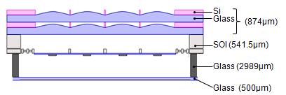
11 Demonstrator I simulating a Mirau Stack Interface A1 Interface B Interface C Interface D Si 200µm Glass 500µm SOI 381µm Glass 500µm Glass 500µm W1 W2 W3 W4 Interface bonding step Alignme nt Interface A1 W1 +/- 8µm Interface B W2+W3 +/- 8µm Interface C W1 + W2/W3 +/- 16µm Interface D W1/W2/W3 + W4 +/- 16µm Summary All anodic bonding
12 Demonstrator II including a mocrolense wafer To decrease bonding times of W2 as well as bonding temperature 15mm Interface A Interface B Interface C Interface D W1 Si, W2 Glass, W3 Glass, W4 Si ~290µm Glass 410µm Si 400µm Glass 500µm Glass 500µm W1: lense wafer W2: Si W3: Glass spacer W4: Glass Al Au/Cr Interface bonding s tep rem arks A Si frame+glass wafer Self-aligning D W3+W4 W3 with DI rinse, W4 with RCA cleaning before bonding C W2+ (W3/W4) W2 with plasma treatment (selective) B W1+(W2/W3/W4) All anodic bonding


 InterfaceD (W4-W3)")
13 Demonstrator II : bond interfaces A B C D W1 Si, W2 Glass, W3 Glass, W4 Interface A Si-Glass lense Bonding temperature: 320 C; Voltage: 500V, 600V S canning Acous tic Micros cope pictures Interface C (W3-W2) InterfaceD (W4-W3) Interface B W1-W2


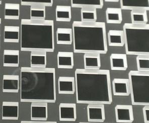
14 Demonstrator II: SEM images of bonded chips W1 W2 cavity W3 bond frame W1 W2 Si Glass Si W4 Cavity of W3 W4 Glass W3 bond frame cavity W4

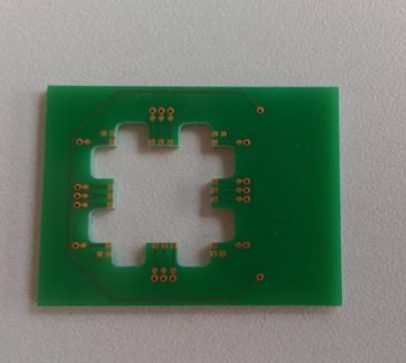
15 Assembly of Mirau µ-interferometer BeamSplitter Plate Mounted on PCB with contact pads

")

16 N-bonding process of a Mirau Stack at chip level Interface bonding step bonding parameters A0, A, A1 lense+lense 350 C. 900V D W3+W4 360 C, 400V (W4 chipwithout TiO2 layer) C W2+ (W3/W4) 360 C, 2000V B W1+(W2/W3/W4) 360 C, 2000V All anodic bonding W2 W1 W3 W4 W3, W4 front side back side back side Infrared camera


 but")
17 N-bonding process of a Mirau Stack at wafer level After bonding at 1000V After bonding at 1100V After bonding at 1100V: Increased bonded area (dark areas) but not significant


 4mm 2nd cutting (i.e.")
18 Laser dicing approach to get Mirau chips front side back side Openings 4mmx4mm A A A A A A 1st cutting (i.e mm) 4mm 2nd cutting (i.e mm) 18


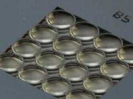
19 Assembled Mirau µ-interferometer 7 wafers to assemble Bonded Mirau s tack Diced chips mounted on PCB
20 Conclusions A suitable design and technology have been demonstrated in order to vertically integrate optically functionalized wafers Demonstrators and Mirau interferometers have been successfully bonded both at chip level and at wafer level. Design of electrical connections for the Mirau interferometer which provides a simple, cost-effective process is proposed and realized. Mirau µ-interferometers are successfully assembled and fully characterized. The assembled Mirau µ-interferometers can be further integrated with other components of an OCT microsystem.


21 Acknowledgement This work is supported by the collaborative project VIAMOS of the European Commission (FP7-ICT , Grant no ). The authors would also like to thank the involved partners


22 Thank you for your attention Contact Wei-Shan Wang Fraunhofer ENAS Department System Packaging 0049 (0) Technologie-Campus Chemnitz Germany
Temporary Wafer Bonding - Key Technology for 3D-MEMS Integration
 Temporary Wafer Bonding - Key Technology for 3D-MEMS Integration 2016-06-15, Chemnitz Chemnitz University of Technology Basic Research Fraunhofer ENAS System-Packaging (SP) Back-End of Line (BEOL) Applied
F R A U N H O F E R I N
 FRAUNHOFER Institute FoR Electronic NAno systems ENAS System Packaging 1 2 3 4 5 The actual developments of micro and nano technologies are fascinating. Undoubted they are playing a key role in today s
HSG-IMIT Application AG
 B4.1 Acceleration Sensors IP-Blocks for MEMS Foundry Surface Micromachining Process R. Knechtel, S. Dempwolf S. Hering X-FAB Semiconductor Foundries AG Haarberstraße 67 99097 Erfurt / Germany T. Link J.
Page Films. we support your innovation
 Page Films we support your innovation Page Films SAES Thin Film Technology: the Evolution of the Getter Integration Pioneering the development of getter technology, the SAES Getters Group is the world
SHRINK. STACK. INTEGRATE.
 SHRINK. STACK. INTEGRATE. SUSS MICROTEC PRODUCT PORTFOLIO SHAPING THE FUTURE With more than 60 years of engineering experience SUSS MicroTec is a leading supplier of process equipment for microstructuring
Low-Temperature Bonding for Silicon-Based Micro-Optical Systems
 Photonics 2015, 2, 1164-1201; doi:10.3390/photonics2041164 Review OPEN ACCESS photonics ISSN 2304-6732 www.mdpi.com/journal/photonics Low-Temperature Bonding for Silicon-Based Micro-Optical Systems Yiheng
LATEST INSIGHTS IN MATERIAL AND PROCESS TECHNOLOGIES FOR INTERPOSER AND 3D STACKING
 LATEST INSIGHTS IN MATERIAL AND PROCESS TECHNOLOGIES FOR INTERPOSER AND 3D STACKING European 3D TSV Summit, January 22-23, 2013, Grenoble Dr. Rainer Knippelmeyer, CTO and VP of R&D, GM Product Line Bonder
Michelson Interferometer. crucial role in Einstein s development of the Special Theory of Relativity.
 Michelson Interferometer The interferometer Michelson experiment Interferometer of Michelson and Morley played 0 a crucial role in Einstein s development of the Special Theory of Relativity. Michelson
EV Group. Enabling processes for 3D interposer. Dr. Thorsten Matthias EV Group
 EV Group Enabling processes for 3D interposer Dr. Thorsten Matthias EV Group EV Group in a Nutshell st Our philosophy Our mission in serving next generation application in semiconductor technology Equipment
Hybrid Wafer Level Bonding for 3D IC
 Hybrid Wafer Level Bonding for 3D IC An Equipment Perspective Markus Wimplinger, Corporate Technology Development & IP Director History & Roadmap - BSI CIS Devices???? 2013 2 nd Generation 3D BSI CIS with
Update in Material and Process Technologies for 2.5/3D IC Dr. Rainer Knippelmeyer CTO and VP R&D, SÜSS MicroTec AG
 Update in Material and Process Technologies for 2.5/3D IC Dr. Rainer Knippelmeyer CTO and VP R&D, SÜSS MicroTec AG TEMPORARY BONDING / DEBONDING AS THIN WAFER HANDLING SOLUTION FOR 3DIC & INTERPOSERS Device
Electrostatic Bonding of Silicon-to-ITO coated #7059 Glass using Li-doped Oxide Interlayer
 Journal of the Korean Physical Society, Vol. 33, No., November 1998, pp. S406 S410 Electrostatic Bonding of Silicon-to-ITO coated #7059 Glass using Li-doped Oxide Interlayer Jee-Won Jeong, Byeong-Kwon
Next-Generation Packaging Technology for Space FPGAs
 Power Matters. Next-Generation Packaging Technology for Space FPGAs Microsemi Space Forum Russia November 2013 Raymond Kuang Director of Packaging Engineering, SoC Products Group Agenda CCGA (ceramic column
FRAUNHOFER INSTITUTE FOR SURFACE ENGINEERING AND THIN FILMS IST ATMOSPHERIC PRESSURE PLASMA PROCESSES
 FRAUNHOFER INSTITUTE FOR SURFACE ENGINEERING AND THIN FILMS IST ATMOSPHERIC PRESSURE PLASMA PROCESSES 1 2 ATMOSPHERIC PRESSURE PLASMA PROCESSES AT THE FRAUNHOFER IST Today, atmospheric pressure plasma
2.76/2.760 Multiscale Systems Design & Manufacturing
 2.76/2.760 Multiscale Systems Design & Manufacturing Fall 2004 MOEMS Devices for Optical communications system Switches and micromirror for Add/drops Diagrams removed for copyright reasons. MOEMS MEMS
Through-Wafer Interconnects for High Degree of Freedom MEMS Deformable Mirrors
 Through-Wafer Interconnects for High Degree of Freedom MEMS Deformable Mirrors Alioune Diouf 1, Thomas G. Bifano 1, Jason B. Stewart 2, Steven Cornelissen 2, Paul Bierden 2 1 Boston University Photonics
Outline. 1 Introduction. 2 Basic IC fabrication processes. 3 Fabrication techniques for MEMS. 4 Applications. 5 Mechanics issues on MEMS MDL NTHU
 Outline 1 Introduction 2 Basic IC fabrication processes 3 Fabrication techniques for MEMS 4 Applications 5 Mechanics issues on MEMS 2. Basic IC fabrication processes 2.1 Deposition and growth 2.2 Photolithography
Final Project Report. Contract/Grant Title: Development of High-Fill-Factor Large-Aperture Micromirrors for Agile Optical Phased Arrays
 Final Project Report Contract/Grant Title: Development of High-Fill-Factor Large-Aperture Micromirrors for Agile Optical Phased Arrays Contract/Grant #: FA9550-08-1-0292 Reporting Period: 1 June 2008 to
Effect of Surface Contamination on Solid-State Bondability of Sn-Ag-Cu Bumps in Ambient Air
 Materials Transactions, Vol. 49, No. 7 (28) pp. 18 to 112 Special Issue on Lead-Free Soldering in Electronics IV #28 The Japan Institute of Metals Effect of Surface Contamination on Solid-State Bondability
Especial Bump Bonding Technique for Silicon Pixel Detectors
 Especial Bump Bonding Technique for Silicon Pixel Detectors E. Cabruja, M. Bigas, M. Ullán, G. Pellegrini, M. Lozano Centre Nacional de Microelectrònica Spain Outline Motivation Summary of bump bonding
Fluxless Soldering in Activated Hydrogen Atmosphere
 Fluxless Soldering in Activated Hydrogen Atmosphere C. Christine Dong1*, Richard E. Patrick1, Russell A. Siminski 1, and Tim Bao 2 1 Air Products and Chemicals, Allentown, PA 18195-1501, USA 2 Air Products
An Investigation on NEG Thick Film for Vacuum packaging of MEMS
 An Investigation on NEG Thick Film for Vacuum packaging of MEMS Y.F. Jin* 1,3, Z.P. Wang 1, L. Zhao 2, P.C. Lim 1, J. Wei 1 1) Singapore Institute of Manufacturing Technology, 71 Nanyang Drive, Singapore
Integrated measuring system for MEMS
 Integrated measuring system for MEMS Thermal characterization of gas flows under slip-flow regime Alice Vittoriosi May 16, 2011 I NSTITUTE FOR M ICRO P ROCESS E NGINEERING - T HERMAL P ROCESS E NGINEERING
Design and Optimization of An All Optically Driven Phase Correction MEMS Device using FEA
 Presented at the COMSOL Conference 2009 Boston Design and Optimization of An All Optically Driven Phase Correction MEMS Device using FEA V. Mathur, K.Anglin, V.S. Prasher, K.Tremkoa, S.R. Vangala, X. Qian,
1
 Process methodologies for temporary thin wafer handling solutions By Justin Furse, Technology Strategist, Brewer Science, Inc. Use of temporary bonding/debonding as part of thin wafer handling processes
ESS 5855 Surface Engineering for. MicroElectroMechanicalechanical Systems. Fall 2010
 ESS 5855 Surface Engineering for Microelectromechanical Systems Fall 2010 MicroElectroMechanicalechanical Systems Miniaturized systems with integrated electrical and mechanical components for actuation
Fiducial Marks for EUV mask blanks. Jan-Peter Urbach, James Folta, Cindy Larson, P.A. Kearney, and Thomas White
 Fiducial Marks for EUV mask blanks Jan-Peter Urbach, James Folta, Cindy Larson, P.A. Kearney, and Thomas White Fiducial marks are laser scribed on 200 mm wafers to enable defect registration on metrology
XBC300 Gen2. Fully-automated debonder and Cleaner
 XBC300 Gen2 Fully-automated debonder and Cleaner XBC300 Gen2 FULLY AUTOMATED DEBONDER AND CLEANER The SUSS XBC300 Gen2 debonder and cleaner platform is designed for process development as well as high
Gaetano L Episcopo. Scanning Electron Microscopy Focus Ion Beam and. Pulsed Plasma Deposition
 Gaetano L Episcopo Scanning Electron Microscopy Focus Ion Beam and Pulsed Plasma Deposition Hystorical background Scientific discoveries 1897: J. Thomson discovers the electron. 1924: L. de Broglie propose
Silicon Capacitive Accelerometers. Ulf Meriheinä M.Sc. (Eng.) Business Development Manager VTI TECHNOLOGIES
 Business Development Manager VTI TECHNOLOGIES") Silicon Capacitive Accelerometers Ulf Meriheinä M.Sc. (Eng.) Business Development Manager VTI TECHNOLOGIES 1 Measuring Acceleration The acceleration measurement is based on Newton s 2nd law: Let the acceleration
Silicon Capacitive Accelerometers Ulf Meriheinä M.Sc. (Eng.) Business Development Manager VTI TECHNOLOGIES 1 Measuring Acceleration The acceleration measurement is based on Newton s 2nd law: Let the acceleration
MEMS Metrology. Prof. Tianhong Cui ME 8254
 MEMS Metrology Prof. Tianhong Cui ME 8254 What is metrology? Metrology It is the science of weights and measures Refers primarily to the measurements of length, weight, time, etc. Mensuration- A branch
OOFELIE::Multiphysics 2014
 OOFELIE::Multiphysics 2014 INDUSTRIAL MULTIPHYSICS DESIGN FOR OPTICAL DEVICES INTRODUCTION 2 High precision opto-mechanics A VERY HIGH ACCURACY IN THE PRODUCTION OF MIRRORS AND LENSES IS NOW VERY OFTEN
ELECTROCHROMIC RADIATORS FOR MICROSPACECRAFT THERMAL CONTROL
 ELECTROCHROMIC RADIATORS FOR MICROSPACECRAFT THERMAL CONTROL Anthony Paris Kevin Anderson Jet Propulsion Laboratory Prasanna Chandrasekhar, Brian Zay, Terrance McQueeney Ashwin-Ushas Corporation, Inc.,
Regents of the University of California
 Deep Reactive-Ion Etching (DRIE) DRIE Issues: Etch Rate Variance The Bosch process: Inductively-coupled plasma Etch Rate: 1.5-4 μm/min Two main cycles in the etch: Etch cycle (5-15 s): SF 6 (SF x+ ) etches
RoHS. Specification CUD8AF1C. 서식 Rev: 00
 Specification RoHS CUD8AF1C 1 [ Contents ] 1. Description 2. Outline dimensions 3. Characteristics of CUD8AF1C 4. Characteristic diagrams 5. Binning & Labeling 6. Reel packing 7. Recommended solder pad
Multi-chip Integration on a PLC Platform for 16X16 Port Optical Switch Using Passive Alignment Technique
 Multi-chip Integration on a PLC Platform for 16X16 Port Optical Switch Using Passive Alignment Technique Jung Woon Lim, Hwe Jong Kim, Seon Hoon Kim and Byung Sup Rho Korea Photonics Technology Institute
Delamination Modeling for Power Packages and Modules. Rainer Dudek, R. Döring, S. Rzepka Fraunhofer ENAS, Micro Materials Center Chemnitz
 Delamination Modeling for Power Packages and Modules Rainer Dudek, R. Döring, S. Rzepka Fraunhofer ENAS, Micro Materials Center Chemnitz The Micro Materials Center @ Virtual Prototyping Finite Element
TITLE: Interferometry: The Michelson Interferometer
 TITLE: Interferometry: The Michelson Interferometer Contributed by: Yolanda Flores Baboquivari High School Summary: The lesson begins with a demonstration introducing students to interference fringes formed
EE C245 ME C218 Introduction to MEMS Design Fall 2007
 EE C245 ME C218 Introduction to MEMS Design Fall 2007 Prof. Clark T.-C. Nguyen Dept. of Electrical Engineering & Computer Sciences University of California at Berkeley Berkeley, CA 94720 Lecture 12: Mechanics
LPSC424.xxx Low Profile Silicon Capacitor
 LPSC424.xxx - 42 Low Profile Silicon Capacitor Rev 3. Key features Ultra low profile (1µm) High stability of capacitance value: Temperature
Deliverable D1.3 Demonstration of patterning processes allowing to
 D.3 H2020-LCE-205- CHEOPS Production technology to achieve low Cost and Highly Efficient photovoltaic Perovskite Solar cells Deliverable D.3 WP Perovskite single junction development Authors: Soo-Jin Moon
Resonator Fabrication for Cavity Enhanced, Tunable Si/Ge Quantum Cascade Detectors
 Resonator Fabrication for Cavity Enhanced, Tunable Si/Ge Quantum Cascade Detectors M. Grydlik 1, P. Rauter 1, T. Fromherz 1, G. Bauer 1, L. Diehl 2, C. Falub 2, G. Dehlinger 2, H. Sigg 2, D. Grützmacher
SURFACE TENSION POWERED SELF-ASSEMBLY OF 3D MOEMS DEVICES USING DRIE OF BONDED SILICON-ON-INSULATOR WAFERS INTRODUCTION
 SURFACE TENSION POWERED SELF-ASSEMBLY OF 3D MOEMS DEVICES USING DRIE OF BONDED SILICON-ON-INSULATOR WAFERS R.R.A Syms, C. Gormley and S. Blackstone Dept. of Electrical and Electronic Engineering, Imperial
Micro- and Nano-Technology... for Optics
 Micro- and Nano-Technology...... for Optics U.D. Zeitner Fraunhofer Institut für Angewandte Optik und Feinmechanik Jena Today: 1. Introduction E. Bernhard Kley Institute of Applied Physics Friedrich-Schiller
Gold nanothorns macroporous silicon hybrid structure: a simple and ultrasensitive platform for SERS
 Supporting Information Gold nanothorns macroporous silicon hybrid structure: a simple and ultrasensitive platform for SERS Kamran Khajehpour,* a Tim Williams, b,c Laure Bourgeois b,d and Sam Adeloju a
ALIGNMENT ACCURACY IN A MA/BA8 GEN3 USING SUBSTRATE CONFORMAL IMPRINT LITHOGRAPHY (SCIL)
") ALIGNMENT ACCURACY IN A MA/BA8 GEN3 USING SUBSTRATE CONFORMAL IMPRINT LITHOGRAPHY (SCIL) Robert Fader Fraunhofer Institute for Integrated Systems and Device Technology (IISB) Germany Ulrike Schömbs SUSS
ALIGNMENT ACCURACY IN A MA/BA8 GEN3 USING SUBSTRATE CONFORMAL IMPRINT LITHOGRAPHY (SCIL) Robert Fader Fraunhofer Institute for Integrated Systems and Device Technology (IISB) Germany Ulrike Schömbs SUSS
Process Analytical Technology Diagnosis, Optimization and Monitoring of Chemical Processes
 FRAUNHOFER INSTITUTe FoR Chemical Technology ICT Process Analytical Technology Diagnosis, Optimization and Monitoring of Chemical Processes Process Analytical Technology Diagnosis, Optimization and Monitoring
DEPOSITION OF THIN TiO 2 FILMS BY DC MAGNETRON SPUTTERING METHOD
 Chapter 4 DEPOSITION OF THIN TiO 2 FILMS BY DC MAGNETRON SPUTTERING METHOD 4.1 INTRODUCTION Sputter deposition process is another old technique being used in modern semiconductor industries. Sputtering
Structuring and bonding of glass-wafers. Dr. Anke Sanz-Velasco
 Structuring and bonding of glass-wafers Dr. Anke Sanz-Velasco Outline IMT Why glass? Components for life science Good bond requirements and evaluation Wafer bonding 1. Fusion bonding 2. UV-adhesive bonding
SCB10H Series Pressure Elements PRODUCT FAMILY SPEFICIFATION. Doc. No B
 PRODUCT FAMILY SPEFICIFATION SCB10H Series Pressure Elements SCB10H Series Pressure Elements Doc. No. 82 1250 00 B Table of Contents 1 General Description... 3 1.1 Introduction... 3 1.2 General Description...
Solder Self-assembly for MEMS
 Solder Self-assembly for MEMS Kevin F. Harsh, Ronda S. Irwin and Y. C. Lee NSF Center for Advanced Manufacturing and Packaging of Microwave, Optical and Digital Electronics, Department of Mechanical Engineering
UVTOP265-HL-TO39. Description. Maximum Rating (T CASE = 25 C) Electro-Optical Characteristics (T CASE = 25 C, I F = 20 ma)
 Electro-Optical Characteristics (T CASE = 25 C, I F = 20 ma)") v3.0 05/17 UVTOP265-HL-TO39 Deep Ultraviolet Light Emission Source 270 nm, 0.6 mw TO39 Package Hemispherical Sapphire Lens Forensic Analysis, Disinfection Description UVTOP265-HL-TO39 is a deep ultraviolet
v3.0 05/17 UVTOP265-HL-TO39 Deep Ultraviolet Light Emission Source 270 nm, 0.6 mw TO39 Package Hemispherical Sapphire Lens Forensic Analysis, Disinfection Description UVTOP265-HL-TO39 is a deep ultraviolet
Passionately Innovating With Customers To Create A Connected World
 Passionately Innovating With Customers To Create A Connected World Multi Die Integration Can Material Suppliers Meet the Challenge? Nov 14, 2012 Jeff Calvert - R&D Director, Advanced Packaging Technologies
Thin Wafer Handling Challenges and Emerging Solutions
 1 Thin Wafer Handling Challenges and Emerging Solutions Dr. Shari Farrens, Mr. Pete Bisson, Mr. Sumant Sood and Mr. James Hermanowski SUSS MicroTec, 228 Suss Drive, Waterbury Center, VT 05655, USA 2 Thin
EV Group. Engineered Substrates for future compound semiconductor devices
 EV Group Engineered Substrates for future compound semiconductor devices Engineered Substrates HB-LED: Engineered growth substrates GaN / GaP layer transfer Mobility enhancement solutions: III-Vs to silicon
MPC-D403 MPC-D404. Ultra-small Peltier Coolers. High impedance Low control current High power efficiency
 MPC-D MPC-D Ultra-small Peltier Coolers High impedance Low control current High power efficiency MPC-D / D. Introduction. General description The MPC- / D micro chip-sized thermoelectric coolers (TEC)
Supplementary information for
 Supplementary information for Transverse electric field dragging of DNA in a nanochannel Makusu Tsutsui, Yuhui He, Masayuki Furuhashi, Rahong Sakon, Masateru Taniguchi & Tomoji Kawai The Supplementary
Supplementary Figure 1: Micromechanical cleavage of graphene on oxygen plasma treated Si/SiO2. Supplementary Figure 2: Comparison of hbn yield.
 1 2 3 4 Supplementary Figure 1: Micromechanical cleavage of graphene on oxygen plasma treated Si/SiO 2. Optical microscopy images of three examples of large single layer graphene flakes cleaved on a single
1. Narrative Overview Questions
 Homework 4 Due Nov. 16, 010 Required Reading: Text and Lecture Slides on Downloadable from Course WEB site: http://courses.washington.edu/overney/nme498.html 1. Narrative Overview Questions Question 1
Problem Solving. radians. 180 radians Stars & Elementary Astrophysics: Introduction Press F1 for Help 41. f s. picture. equation.
 Problem Solving picture θ f = 10 m s =1 cm equation rearrange numbers with units θ factors to change units s θ = = f sinθ fθ = s / cm 10 m f 1 m 100 cm check dimensions 1 3 π 180 radians = 10 60 arcmin
Nonlinear Time and Temperature Dependent Analysis of the Lead-Free Solder Sealing Ring of a Photonic Switch
 Nonlinear Time and Temperature Dependent Analysis of the Lead-Free Solder Sealing Ring of a Photonic Switch J. Lau, Z. Mei, S. Pang, C. Amsden, J. Rayner and S. Pan Agilent Technologies, Inc. 5301 Stevens
1 INTRODUCTION 2 SAMPLE PREPARATIONS
 Chikage NORITAKE This study seeks to analyze the reliability of three-dimensional (3D) chip stacked packages under cyclic thermal loading. The critical areas of 3D chip stacked packages are defined using
MINIATURIZATION TECHNOLOGIES FOR DEPLOYABLE SYSTEMS
 MINIATURIZATION TECHNOLOGIES FOR DEPLOYABLE SYSTEMS MEMS, MICROSENSORS, AND NANOTECHNOLOGY Harish Manohara NANO AND MICRO SYSTEMS GROUP Jet Propulsion Laboratory 4800 Oak Grove Drive Pasadena, CA 91109
Micro/nano and precision manufacturing technologies and applications
 The 4th China-American Frontiers of Engineering Symposium Micro/nano and precision manufacturing technologies and applications Dazhi Wang School of Mechanical Engineering Dalian University of Technology
PHI. Scanning XPS Microprobe
 PHI Scanning XPS Microprobe Unique Scanning XPS Microprobe X-ray photoelectron spectroscopy (XPS/ESA) is the most widely used surface analysis technique and has many well established industrial and research
Advanced laser technology for 3D-shaping ~ toward to the highest brightness of electron beam source ~
 Advanced laser technology for 3D-shaping ~ toward to the highest brightness of electron beam source ~ Hiromistu Tomizawa Accelerator Division, Japan Synchrotron Radiation Research Institute (SPring-8)
HBM fine pitch micro pillar grid array probing evaluation
 HBM fine pitch micro pillar grid array probing evaluation Raffaele Vallauri, Technoprobe Daniele Perego, Technoprobe Marco Prea, Technoprobe Jaehong Kim, Samsung Electronics Jinyeong Yun, Samsung Electronics
Self-Alignment with Copper Pillars Micro-Bumps for Positioning Optical Devices at Submicronic Accuracy
 2017 IEEE 67th Electronic Components and Technology Conference Self-Alignment with Copper Pillars Micro-Bumps for Positioning Optical Devices at Submicronic Accuracy Yézouma D. Zonou, Stéphane Bernabé,
Nanomotion Precision Piezo Ceramic Motors
 Nanomotion Precision Piezo Ceramic Motors The Company Nanomotion was founded in 1992 Developed enabling technology for ultrasonic piezo-ceramic motors Entered the market in 1996, selling products to leading
Polarization control and sensing with two-dimensional coupled photonic crystal microcavity arrays. Hatice Altug * and Jelena Vučković
 Polarization control and sensing with two-dimensional coupled photonic crystal microcavity arrays Hatice Altug * and Jelena Vučković Edward L. Ginzton Laboratory, Stanford University, Stanford, CA 94305-4088
Introduction to Microeletromechanical Systems (MEMS) Lecture 9 Topics. MEMS Overview
 Lecture 9 Topics. MEMS Overview") Introduction to Microeletromechanical Systems (MEMS) Lecture 9 Topics MicroOptoElectroMechanical Systems (MOEMS) Grating Light Valves Corner Cube Reflector (CCR) MEMS Light Modulator Optical Switch Micromirrors
Introduction to Microeletromechanical Systems (MEMS) Lecture 9 Topics MicroOptoElectroMechanical Systems (MOEMS) Grating Light Valves Corner Cube Reflector (CCR) MEMS Light Modulator Optical Switch Micromirrors
Development of low cost set up for anodic bonding and its characterization
 Indian Journal of Pure & Applied Physics Vol. 46, October 2008, pp. 738-743 Development of low cost set up for anodic bonding and its characterization C C Tripathi +, Shruti Jain +, Pawan Joshi +, S C
1 Naval Research Laboratory Remote Sensing Division, Code Aberdeen Ave SE Kirtland AFB, NM 87117
 Carbon Fiber Reinforced Polymer (CFRP) Telescope Program at the Naval Research Laboratory Sergio R. Restaino 1, Ty Martinez 1, Jonathan R. Andrews 1, Christopher C. Wilcox 1, S. Teare 2, Robert Romeo 3,
Performance, Packaging, Price: Challenges for Sensor Research I. Eisele Fraunhofer EMFT
 Performance, Packaging, Price: Challenges for Sensor Research I. Eisele Fraunhofer EMFT Introduction There are many sensor effects... but only a a very few sensors! Outline CMOS Encapsulated CMOS/MEMS
JRA3: Technology development for high-time-resolution astronomy
 JRA3: Technology development for high-time-resolution astronomy ( HTRA: ~ 10 ms -- 1μs ) Objectives: - To develop the most promising technologies for HTRA - Assess relative strengths/areas of application
Lecture 23 Optical MEMS (5)
") EEL6935 Advanced MEMS (Spring 2005) Instructor: Dr. Huikai Xie Lecture 23 Optical MEMS (5) Agenda: Microlenses Diffractive Microgratings Example Devices Reference: S. Sinzinger and J. Jahns, Chapter 6
EEL6935 Advanced MEMS (Spring 2005) Instructor: Dr. Huikai Xie Lecture 23 Optical MEMS (5) Agenda: Microlenses Diffractive Microgratings Example Devices Reference: S. Sinzinger and J. Jahns, Chapter 6
No. 3, Gongye E. 3rd Road, Hsinchu Science Park, Hsinchu 30075, Taiwan TEL: Lextar.com PC56H01 V4. Product Specification
 Lextar.com Product Specification Approval Sheet Product Specification Product Part Number White SMD LED Issue Date 2013/11/01 Feature White SMD LED (L x W x H) of 5.6 x 3.0 x 0.77 mm ASNI binning Dice
Integrating MEMS Electro-Static Driven Micro-Probe and Laser Doppler Vibrometer for Non-Contact Vibration Mode SPM System Design
 Tamkang Journal of Science and Engineering, Vol. 12, No. 4, pp. 399 407 (2009) 399 Integrating MEMS Electro-Static Driven Micro-Probe and Laser Doppler Vibrometer for Non-Contact Vibration Mode SPM System
Features. ProLight PM6B-3LFx 3W RGB Power LED Technical Datasheet Version: /03
 ProLight PM6B-3LFx 3W RGB Power LED Technical Datasheet Version: 1.7 Features R, G, B three color in one Package High flux per LED Good color uniformity Lead free reflow soldering More energy efficient
Optimization of Process Parameters for Micropart Capillary Assembly with Precision Positioning
 Optimization of Process Parameters for Micropart Capillary Assembly with Precision Positioning Andrew X. Zhou, 1 Shaghayegh Abbasi, 2 Rajashree Baskaran, 2 Karl F. Böhringer 2 1 Department of Bioengineering,
Technical Note ITER Bolometer sensors
 Technical Note ITER Bolometer sensors Introduction The manufacture of bolometer sensors currently envisaged for ITER makes use of thin-film technologies. This Technical Note describes the characteristics
New Requirements for Sir- Measurement
 New Requirements for Sir- Measurement Jörg Trodler Heraeus Materials Technology GmbHo.KG Hanau, Germany Joerg.trodler@heraeus.com Mathias Nowottnick, Prof. University of Rostock Rostock, Germany Abstract
Development of High-Z Semiconductor Detectors and Their Applications to X-ray/gamma-ray Astronomy
 Development of High-Z Semiconductor Detectors and Their Applications to X-ray/gamma-ray Astronomy Taka Tanaka (SLAC/KIPAC) 9/19/2007 SLAC Advanced Instrumentation Seminar Outline Introduction CdTe Diode
WTSC144.xxx Wire Bonding Temperature Silicon Vertical Capacitor
 WTSC144.xxx Wire Bonding Temperature Silicon Vertical Capacitor Rev 3.1 Key features Full compatible to monolithic ceramic capacitors Ultra high stability of capacitance value: Temperature ±1.5% (-55 C
Coatings for CO Laser Optics
 Coatings for CO Laser Optics ULO Optics is the leading European manufacturer of CO laser optics, a position it has held for more than two decades. The optics manufactured by ULO Optics are often used in
MSE 321 Structural Characterization
 Auger Spectroscopy Auger Electron Spectroscopy (AES) Scanning Auger Microscopy (SAM) Incident Electron Ejected Electron Auger Electron Initial State Intermediate State Final State Physical Electronics
TRENDS IN LEVENSDUURTESTEN VOOR MICRO-ELEKTRONICA PLOT CONFERENTIE
 TRENDS IN LEVENSDUURTESTEN VOOR MICRO-ELEKTRONICA PLOT CONFERENTIE JEROEN JALINK 8 JUNI 2016 MICROELECTRONICS RELIABILITY 54 (2014) 1988 1994 Contents Introduction NXP Package form factor Failure mechanism
Other SPM Techniques. Scanning Probe Microscopy HT10
 Other SPM Techniques Scanning Near-Field Optical Microscopy (SNOM) Scanning Capacitance Microscopy (SCM) Scanning Spreading Resistance Microscopy (SSRM) Multiprobe techniques Electrostatic Force Microscopy,
Simple piezoresistive accelerometer
 Simple piezoresistive pressure sensor Simple piezoresistive accelerometer Simple capacitive accelerometer Cap wafer C(x)=C(x(a)) Cap wafer may be micromachined silicon, pyrex, Serves as over-range protection,
A Multipass Optics for Quantum-Well-Pumped Semiconductor Disk Lasers
 Multipass-Pumped Semiconductor Disk Lasers 37 A Multipass Optics for Quantum-Well-Pumped Semiconductor Disk Lasers Markus Polanik The pump absorption of quantum-well-pumped semiconductor disk lasers can
TTC-1001 Thermal Test Chip Application Information
 TTC-1001 Thermal Test Chip Application Information Thermal Engineeringa Associates 3287 Kifer Road Santa Clara, CA 95051 Tel: 650-961-5900 Email: info@thermenger.com www.thermengr.com Rev. 4 160125 TTC-1001
Low Voltage Field Emission SEM (LV FE-SEM): A Promising Imaging Approach for Graphene Samples
: A Promising Imaging Approach for Graphene Samples") Low Voltage Field Emission SEM (LV FE-SEM): A Promising Imaging Approach for Graphene Samples Jining Xie Agilent Technologies May 23 rd, 2012 www.agilent.com/find/nano Outline 1. Introduction 2. Agilent
Low Voltage Field Emission SEM (LV FE-SEM): A Promising Imaging Approach for Graphene Samples Jining Xie Agilent Technologies May 23 rd, 2012 www.agilent.com/find/nano Outline 1. Introduction 2. Agilent
Parameter Identification of Pressure Sensors by Static and Dynamic Measurements
 Parameter Identification of Pressure Sensors by Static and Dynamic Measurements S. Michael, S. Kurth, J. Klattenhoff, H. Geissler, S. Hering To cite this version: S. Michael, S. Kurth, J. Klattenhoff,
Crystalline Surfaces for Laser Metrology
 Crystalline Surfaces for Laser Metrology A.V. Latyshev, Institute of Semiconductor Physics SB RAS, Novosibirsk, Russia Abstract: The number of methodological recommendations has been pronounced to describe
A tutorial on meta-materials and THz technology
 p.1/49 A tutorial on meta-materials and THz technology Thomas Feurer thomas.feurer@iap.unibe.ch Institute of Applied Physics Sidlerstr. 5, 3012 Bern Switzerland p.2/49 Outline Meta-materials Super-lenses
3D Micropatterned Surface Inspired by Salvinia
 Supporting information 3D Micropatterned Surface Inspired by Salvinia molesta via Direct Laser Lithography. Omar Tricinci*,, Tercio Terencio,#, Barbara Mazzolai, Nicola M. Pugno,,, Francesco Greco*,, Virgilio
A vibrating micro-cmm probe for micropart metrology
 Microparts meeting - NPL 28 th October 2009 A vibrating micro-cmm probe for micropart metrology Richard Leach A vibrating micro-cmm probe for micro-part metrology Introduction Measuring co-ordinate geometry
Part Qualification/Upscreen:
 Part Qualification/Upscreen: The customer had a series of environmental processes to which their devices needed to be qualified. A nondestructive method of evaluating the devices for any changes caused
STANDARD: SPECIFICATION FOR PROTECTIVE ENCLOSURE AND CARRIER SYSTEMS USED TO TRANSPORT AND STORE ( INCH EUV RETICLES
 Entegris Edit -SEMI Draft Document (10-11-2006 Revision) NEW STANDARD: SPECIFICATION FOR PROTECTIVE ENCLOSURE AND CARRIER SYSTEMS USED TO TRANSPORT AND STORE 6 INCH EUV RETICLES This specification draft
High Efficiency Triple-Junction Solar Cells Employing Biomimetic Antireflective Structures
 High Efficiency Triple-Junction Solar Cells Employing Biomimetic Antireflective Structures M.Y. Chiu, C.-H. Chang, F.-Y. Chang, and Peichen Yu, Green Photonics Laboratory Department of Photonics National