Ionized physical vapor deposition (IPVD): A review of technology and applications
|
|
|
- Clyde Lee
- 5 years ago
- Views:
Transcription
1 Ionized physical vapor deposition (IPVD): A review of technology and applications Ulf Helmersson, Martina Lattemann, Johan Böhlmark, Arutiun P. Ehiasarian and Jon Tomas Gudmundsson The self-archived postprint version of this journal article is available at Linköping University Institutional Repository (DiVA): N.B.: When citing this work, cite the original publication. Helmersson, U., Lattemann, M., Böhlmark, J., Ehiasarian, A. P., Gudmundsson, J. T., (2006), Ionized physical vapor deposition (IPVD): A review of technology and applications, Thin Solid Films, 513(1-2), Original publication available at: Copyright: Elsevier
2 Ionized Physical Vapor Deposition (IPVD): A Review of Technology and Applications Ulf Helmersson, Martina Lattemann, and Johan Bohlmark IFM Materials Science, Linköping University, SE Linköping, Sweden Arutiun P. Ehiasarian Materials and Engineering Research Institute, Sheffield Hallam University, Howard St, Sheffield, S1 1WB, UK Jon Tomas Gudmundsson Department of Electrical and Computer Engineering, University of Iceland, Reykjavik, Iceland and Science Institute, University of Iceland, Reykjavik, Iceland Keywords Ionized physical vapor deposition; Sputtering; Plasma processing and deposition; Arc-evaporation Abstract In plasma-based deposition processing, the importance of low-energy ion bombardment during thin film growth can hardly be exaggerated. Ion bombardment is an important physical tool available to materials scientists in the design of new materials and new structures. Glow discharges and in particular the magnetron sputtering discharge have the advantage that the ions of the discharge are abundantly available to the deposition process. However, the ion chemistry is usually dominated by the ions of the inert sputtering gas while ions of the sputtered material are rare. Over the past few years, various ionized sputtering techniques have appeared that can achieve a high degree of ionization of the sputtered atoms, often up to 50 % but in some cases as much as approximately 90%. This opens a complete new perspective in the engineering and design of new thin film materials. The development and application of magnetron sputtering systems for ionized physical vapor deposition (IPVD) is reviewed. The application of a secondary discharge, inductively coupled plasma 1
3 magnetron sputtering (ICP-MS) and microwave amplified magnetron sputtering, is discussed as well as the high power impulse magnetron sputtering (HIPIMS), the self-sustained sputtering (SSS) magnetron, and the hollow cathode magnetron (HCM) sputtering discharges. Furthermore, filtered arc-deposition is discussed due to its importance as an IPVD technique. Examples of the importance of the IPVD-techniques for growth of thin films with improved adhesion, improved microstructures, improved coverage of complex shaped substrates, and increased reactivity with higher deposition rate in reactive processes are reviewed. 1. Introduction 2. Metal ionization a simple model 3. Magnetron sputtering 3.1 Inductively coupled plasma magnetron sputtering (ICP-MS) Plasma parameters 3.2 Microwaves amplified magnetron sputtering (ECR-MS) 3.3 High power impulse magnetron sputtering (HIPIMS) Electrical parameters and power supply Plasma parameters Degree of ionization Deposition rate 3.4 Self-sustained sputtering (SSS) 3.5 Hollow cathode magnetron (HCM) sputtering 4. Filtered cathodic arc 5. Applications of ionized magnetron sputtering 5.1 Microstructure control by low-energy ion bombardment 5.2 Guiding of material flux and selective deposition 5.3 Interface engineering by substrate pretreatment 5.4 Reactive sputtering 7. Summary References 2
4 1. Introduction Deposition of thin films by physical vapor deposition (PVD) techniques has found widespread use in many industrial sectors. State of the art magnetron sputtering processes allow the deposition of metals, alloys, ceramic, and polymer thin films onto a wide range of substrate materials. Therefore, it is used for a wide field of coating applications for, e.g., metal-working industry, biomedical applications, and optical or electrical components. There is an increasing demand for coatings with tailored and enhanced properties such as high hardness, wear and corrosion resistance, low friction, and specific optical or electrical properties as well as decorative colors and often complex combinations of those properties are requested. For high-quality coating on temperaturesensitive substrates such as polymers, there is room for improvements using versatile PVD techniques. Furthermore, magnetron sputtering offers the possibility to synthesize materials outside thermodynamic equilibrium. Thus, it enables the deposition of metastable phases. The field of applications includes integrated circuit (IC) manufacturing applications such as the formation of diffusion barriers, and adhesion and seed layers on the side and bottom of high aspect ratio vias and trenches. With the fast development of the microelectronics industry in which the circuit dimensions shrink steadily, increasing the aspect ratio, successful coverage using magnetron sputtering becomes increasingly more challenging. The increased requirements on coating materials and the synthesis technique as well as the opening of new fields, therefore drive the development of enhanced deposition techniques allowing direct control of the sputtered flux and further decrease in the deposition temperature, by enhancing the adatom mobility through the momentum transfer to the film, and an increased chemical reactivity. Glow discharge methods like magnetron sputtering have the advantage that the ions of the discharge are abundantly available to the deposition process. However, the ions available are mainly the ions of the inert sputtering gas and ions of the sputtered material are rare. Over the last few years various ionized sputtering techniques have appeared that can achieve a high degree of ionization of the sputtered atoms. This review is focused on the recent development of ionized PVD (IPVD) processes and applications. When the deposition flux consists of more ions than neutrals or ΓM+ > ΓM the process is referred to as IPVD [1]. The development of IPVD-techniques was initially mainly driven by the 3
5 need to deposit metal layers and diffusion barriers into trenches or vias of high aspect ratio IC structures [2-5], but has during the past years found a number of additional areas where beneficial properties are observed. The motion of neutral atoms is difficult to control but ions can be collimated by an electric field. A thin positively charged layer called sheath is formed near surfaces immersed in a plasma. The ions that enter the sheath region are thus accelerated towards the substrate and collimated due to the electric field across the sheath. Furthermore, the ion bombardment energy can be controlled by applying a bias voltage to the substrate. Because of the collimation, the ions may reach the bottom of deep narrow trenches or vias, while a neutral flux will tend to deposit on the upper part of sidewalls leaving the bottom with very little film coverage and possibly a void formation at the bottom of the trench. Thus, IPVD enhances step coverage, both bottom and lower sidewall coverage. Furthermore, ionizing the sputtered vapor has several advantages: improvement of the film quality, such as density and adhesion, especially for substrates of complex shape [6, 7], control of the reactivity, extending the metallic sputtering mode regime [8-10], decreasing the deposition temperature [11], and guiding of the deposition material to the desired areas of the substrate [12]. Many different IPVD-techniques are available today. This review focuses on the fundamental aspects of ionization, on magnetron sputtering techniques and, in particular, the high power impulse magnetron sputtering discharge (HIPIMS). A non-sputtering IPVD-technique is also included in this review, which is cathodic arc deposition. The importance of the IPVD-techniques for the growth of thin films is demonstrated with examples of improved adhesion, improved microstructures, improved coverage of complex shaped substrates, increased reactivity and higher deposition rate in reactive processes. 2. Metal ionization a simple model Processing plasmas consist of both charged and neutral particles, and are generally referred to as weakly ionized plasmas [13]. In such a plasma, collisions of the charged particles with neutral gas atoms are of great significance and ionization of neutrals sustains the plasma in steady state. The plasma is characterized by the density and temperature of each specie and the electrons are usually not in thermal equilibrium with the neutral species and ions. These discharges are electrically driven and the applied power preferentially heats the more mobile electrons. Therefore, the electron 4
6 temperature Te can be significantly higher than the ion temperature. In a weakly ionized discharge, the electron density ne and the ion density ni are generally a few orders of magnitude lower than the neutral gas density of the inert sputtering gas. To explore the plasma parameters and the ionization mechanism for highly ionized magnetron sputtering a simple global model was developed by Hopwood and Qian [2, 14]. Their model gives an estimate of the fractional ionization as well as the ionization process for various conditions in the IPVD process. The discharge is assumed to consist of electrons, Ar atoms in the ground state, metastable Ar atoms, Ar + ions, metal atoms, M, and metal ions, M +. In the model, it is assumed that metal ions are generated by electron impact ionization e + M M + + 2e and by Penning ionization by collision with a metastable excited Ar atom Ar* + M M + + Ar + e with the rate coefficients kmiz and kp, respectively. The metal ions are assumed to be lost by diffusion to solid surfaces such as the chamber walls. The steady state particle balance equation for the metal ions is thus k miz n n e M + k n p Ar n n = τ + M * (1) M M + where nm is the neutral metal density, nm+ is the metal ion density, nar* is the density of metastable Ar atoms and τm+ is the lifetime of the metal ions in the discharge and is determined by the ambipolar diffusion coefficient of the metal ions. Penning ionization depends on the density of the metastable Ar atoms which are produced by electron impact excitation e + Ar Ar* + e with rate coefficient kex and the loss of the metastable Ar atoms is due to deexcitation by Penning ionization, radiative decay, diffusion losses, and electron impact ionization e + Ar* Ar + + e with rate coefficient kiz*. The particle balance equation for generation and loss of metastable Ar atoms is, therefore, k ex n n e Ar = n Ar* 1 [ k n + k n + ] iz* e p M n Ar τ * τ Ar* where τar* is the lifetime of excited Ar. From equations (1) and (2), the metal ion fraction in the discharge is given as n M M ( kmiz + k pkexτ nar ) τ + n M e + ( kmiz + k pkexτ nar ) + ne n + M = + n 1 τ + M The electron temperature Te is self-consistently determined by adding the quasi-neutrality condition = n + + n + M n (4) e Ar (2) (3) 5
7 and particle balance for Ar ions k iz n n e Ar + k iz n n n = + Ar * e Ar* (5) τ + Ar where kiz is the rate coefficient for the single-step ionization process e + Ar Ar + + 2e and τar+ is the lifetime of Ar ions in the discharge. The lifetime is determined by the loss of Ar ions to the wall. The rate coefficient for ionization of Ar is expressed in the Arrhenius form koexp(-eo/te). Since nar >> nm the electron temperature is determined by the particle balance for the Ar plasma from Eq. (5) [14]. The set of equations is solved for the specified Ar pressure, neutral gas temperature, and chamber geometry. By applying this model, Hopwood [2] demonstrated that for low electron density (ne << m -3 ), Penning ionization is the dominating process for metal ionization, whereas for high electron density (ne >> m -3 ) the metal ions are generated by electron impact ionization. At high electron density, metastable Ar atoms are rapidly lost by collisions with electrons. A high level of metal ionization is to be expected in this case since the metal species commonly used (Cu, Ti, Al, Ta) have ionization potentials in the range 6-8 ev which is significantly lower than for the used inert sputtering gas atoms commonly used. The ionization potential of some metal atoms and gases are listed in Table I. The metal is thus efficiently ionized by the energetic electrons required to maintain the Ar plasma. The rate coefficient for electron impact ionization for some widely used, important metals is given in Table II. This model has also been extended to describe reactive sputtering of Ti in Ar/N2 discharge [16]. In the application of plasmas for thin film deposition, the fluxes of the depositing species are of primary importance. The plasmas, which are quasi-neutral, are joined to wall surfaces across thin positively charged layers referred to as sheaths. The metal ion flux at the surface takes into account the acceleration of the ions across the sheath where Γ u (6) M + n + M 1 2 B kbte u = B (7) + mm is the Bohm velocity and mm+ is the metal ion mass. The flux of the neutral metal, on the other hand, is determined by the thermal velocity νm: 6
8 where Γ MM + = 1 4 νν MMnn MM (8) νν MM = 8kk BBTT gg 1 2 ππmm MM is the mean thermal velocity of the gas. Thus Γ MM + Γ MM TT 1 2 ee TT gg where Tg is the neutral gas temperature. In discharges that are not in thermal equilibrium, Te is typically significantly larger than Tg. Thus, the fraction of ionized metal flux at the substrate is larger than the fraction of ionized metal in the plasma n M n + M + + n M (9) (10) Γ MM + Γ MM ++Γ MM. Figure 1 shows the ionized flux fraction versus electron density for various elements. For low electron densities of ~ m -3, the ion fraction is of the order of few percent as commonly observed in a conventional magnetron sputtering discharge. For a high electron density of the order of m -3, as achieved in inductively coupled discharges and electron cyclotron discharges, the ionized flux fraction of Ti is ~ 80 %, Al ~ 65%, and for Cu ~ 35%. That the ionized flux fraction of Al is lower than for Ti is at a first sight surprising, but it is due to the relatively lower rate coefficient for Al. In summary, the dense background plasma is the key to achieve the highly ionized flux fraction, and the obtained fluxes for the different elements depend on ionization potential, mass, and ionization rate coefficient. 3. Magnetron sputtering Direct current magnetron sputtering (dcms) is a widely used technique for deposition of metal and compound layers for numerous technical applications. As an example, the microelectronic industry uses sputtering for deposition of metal or metal compounds as layers for diffusion barriers, adhesion or seed layers, primary conductors, etc. [4, 5]. dcms is a plasma technique utilizing magnetic fields to enhance and confine the plasma close to the deposition source. The deposition species are vaporized by sputtering from the target (the cathode) by ion bombardment. In a conventional magnetron sputtering discharge, only a small fraction of the sputtered atoms are ionized, roughly of the order of one or a few %. In dcms, the vapor is considerable more energetic than 7
9 thermally evaporated atoms (a few ev as compared to about a tenth of an ev). Usually it is desirable to maintain this initial kinetic energy of the sputtered atoms, because of its effect on the film growth. Relatively low pressures are normally used to minimize scattering of the sputtered atoms. The sputtering process is, therefore, normally a line-of-sight process where the deposition flux, since it consists of neutral atoms, cannot be easily controlled. In a conventional dcms discharge, the cathode is kept at a constant negative voltage. Positive ions generated in the plasma are accelerated towards the cathode, sputtering atoms and molecules from the target surface. The main difference between a conventional glow discharge [17] and a magnetron discharge is the presence of an externally applied magnetic field in the latter [18, 19]. The magnetic field can be created by permanent magnets [18], electromagnets [20] or a combination of both [21]. This configuration acts to trap electrons. Thus, in a magnetron sputtering discharge, atoms are sputtered from the cathode target by a magnetically confined plasma. The target material is sputtered by the bombardment of high energy ions accelerated over the cathode sheath potential. Secondary electrons are emitted and accelerated away from the target surface as a result of the ion bombardment. These electrons play an important role in maintaining the plasma. A magnetic field confines the ionizing energetic electrons near the cathode allowing operation at high plasma densities and low pressures. The plasma is efficiently confined near the magnetron target, but the substrate usually lies in a weak plasma which can be enhanced by unbalancing the magnetic field to leak hot electrons [20, 22]. A typical direct current (dc) planar magnetron operates at a pressure of 1-10 mtorr with a magnetic field strength of T and at cathode potentials V. This leads to current densities below 100 ma cm -2 and power densities of up to 50 W cm -2 [19, 23]. For special designs, giving improved cooling, such as rotating cylindrical target with a fixed magnetic assembly [24] and rotating magnet assembly [25], or the use of increased cooling [26, 27], higher current densities can be achieved. The cathode current voltage characteristics are found to follow the relationship Id = kdvd n (11) where Id is the cathode discharge current and Vd the cathode voltage and n is in the range between 3 and 15 [23, 28]. The exponent n depends on the efficiency of the electron trapping in the plasma. The 8
10 higher the value n, the more efficient is the electron trapping. The lower values are found when operating at low pressures or by a weak magnetic field [28-30]. The constant kd depends on the target material, gas pressure, gas type, and the geometry of the discharge. There is a general interest in developing the conventional magnetron sputtering processes to increase metal ionization, target utilization, avoid target poisoning in reactive sputtering, increase deposition rates, especially for dielectric and ferromagnetic materials, and to minimize electrical instabilities such as arcs. For a typical magnetron, there is an interdependence of the target voltage and target current. Increased deposition rate requires increased target voltage to achieve a higher plasma density. This leads to a higher ion flux, which in turn increases the target current. Furthermore, the plasma density increases with increased power. But increased power leads to overheating and eventually melting of the sputtering target. Thus, there is an upper limit to the power that can be delivered to the discharge target. Several sputtering systems have been designed to improve on the conventional magnetron sputtering. Some improvements have been alleviated by pulsing the applied voltage [31, 32], others by additional ionization by radio frequency (rf) [3, 33] or microwave power [34, 35], or by an increased magnetic confinement [36]. The conventional planar magnetron discharge has been discussed in reviews by Waits [19] and Rossnagel [37]. Recent developments in magnetron sputtering technology are reviewed by Kelly and Arnell [38] and by Schneider et al. [39]. Recently, magnetron sputtering discharges have been developed to generate highly ionized plasmas using essentially the conventional magnetron sputtering equipment. Ionized magnetron sputtering processes were initially based on the application of a secondary discharge to create a dense plasma between the source and the substrate so that a large fraction of the sputtered atoms are ionized in agreement with the processes described in section 2. The first sputter-based IPVD systems consisted of a magnetron cathode for physical sputtering of atoms and a secondary discharge which could be either inductively coupled plasma [3, 33] or microwave driven discharges [34, 40-42]. Other methods of creating highly ionized sputtered vapor include shaping the cathode target in a particular way in order to confine the electrons, referred to as hollow cathode magnetron discharge [43, 44] or the application of high powers. Here, the development of magnetron sputtering discharges for the creation of a high fraction of ionized sputtered species is reviewed. First, the application of a 9
11 secondary discharge between the target and the substrate is discussed, an inductively coupled discharge in section 3.1, and a microwave amplified discharge in section 3.2. The main emphasis is on the high power impulse magnetron sputtering discharge which is discussed in section 3.3. The self-sustained sputtering (SSS) discharge is discussed in section 3.4, and the hollow cathode magnetron (HCM) discharge in section Inductively coupled plasma magnetron sputtering (ICP-MS) In order to generate a highly ionized discharge, an inductively coupled plasma (ICP) source can be added in the region between the cathode and the substrate. A non-resonant induction coil is then placed parallel to the cathode, in essentially a conventional dcms apparatus, immersed or adjacent to the plasma as seen in Fig. 2. The inductive coil is generally driven at MHz using a 50 Ω rf power supply through a capacitive matching network [45]. The rf power is often coupled to the plasma across a dielectric window or wall. Inductively coupled discharges are commonly operated in the pressure range 1 50 mtorr and applied power W resulting in an electron density in the range of m -3, generally found to increase linearly with increasing applied power [45-47]. In a magnetron sputtering discharge the metal atoms are sputtered from the cathode target using dc or rf power and transit the dense plasma, created by the rf coil, where they are ionized [3, 33]. The plasma parameters and their dependence on rf power in an ICP-MS discharge have been measured by several groups [14, 48-51]. In general, it is found that the ionization, and therefore the ionization flux fraction, increases with increased rf power and pressure. Wang et al. [48, 49] investigated the plasma parameters in an Ar discharge with a Cu target. Fig. 3 shows the ion density versus the applied rf power. Generally it is found that at constant dc cathode power and constant pressure the relative ionization increases and saturates as the inductively coupled rf power is increased [3, 49]. The ionized flux fraction for Cu versus applied rf power for Ar discharge at 20 and 40 mtorr is shown in Fig. 4. Li et al. [52] demonstrated that the ion energy distribution in an ICP-MS discharge is 10
12 relatively narrow and mainly determined by the plasma potential. This indicated that the ion flux and the ion energy could be controlled independently by varying the applied rf power and the substrate bias voltage independently. This is a great advantage over a conventional dcms discharge where the ion flux and the ion bombarding energy cannot be varied independently without changing the magnetic configuration. The ion energy distribution at the substrate for Ar + and N2 + ions are shown in Figs. 5 (a) and (b), respectively, using a Ti target. When no power was applied to the induction coil a sharp, but relatively weak peak, appears at roughly 3.6 ev. As the discharge is enhanced by the additional rf power, the ion peak energy was shifted to a higher values of about 22 ev, mainly due to the increase in the plasma potential. With further increase in the rf power, the peak energy remained roughly constant. Thus, the sheath potential is determined by the plasma potential which only depends on the gas pressure and the gas type. 3.2 Microwave amplified magnetron sputtering Another approach to increase ionization of the sputtered metal is to use a supplementary electron cyclotron resonance (ECR) discharge giving high plasma densities ( m -3 ) commonly operated at low working pressures ( mtorr) while maintaining low plasma potentials [45, 53]. The low plasma potential allows the possibility to control the ion energy. ECR discharges are typically operated at microwave frequencies (e.g. ~2.45 GHz) with a strong magnetic field. In an ECR discharge, a right-hand circularly polarized wave propagates along steady magnetic field lines to a resonance zone. There, the wave energy is absorbed by a collisionless heating mechanism. The introduction of a magnetic field leads to a resonance between the applied frequency ω and the electron cyclotron frequency ωce = eb/me within the discharge. Due to this cyclotron resonance, the gyrating electrons rotate in phase with the polarized wave. Holberg et al. [54] used an ECR discharge to ionize Cu that was evaporated from a resistively heated source. They realized a Cu discharge which was nearly 100% ionized and demonstrated its usefulness in high aspect ratio metal filling. Magnetron sputtering discharges, where a microwave discharge is operated in ECR mode to increase the ionization of the metal species (ECR-MS), have also been developed [34, 35, 40, 41, 55, 56]. In general, an ECR discharge produces significantly 11
13 higher density plasma (~ m -3 ) than a dcms discharge (~ m -3 ). Fig. 6 is a schematic diagram of the apparatus used by Xu et al. [40] and Li et al. [55]. The two ECR discharge chambers are located at opposite sides of the main processing chamber. The magnetic coils are arranged around the periphery of each of the ECR discharge chambers and the currents in these coils flow in opposite direction generating a magnetic field of 875 G to satisfy the ECR condition in both ECR chambers. Thus, a highly ionized ECR plasma is created in the region between the target and the substrate. A configuration described by Takahashi et al. [35] is shown in Fig. 7 and consists of a plasma chamber that operates as a microwave cavity resonator. Microwave power (2.45 GHz) is introduced through a rectangular waveguide and a fused quartz window. The magnetic coils are arranged around the chamber periphery to achieve ECR conditions. The sputtering target is placed at the plasma extraction window around the extracted plasma stream with a shield electrode. The target is connected to a dc power supply. The top and the bottom rings around the target are made of iron which effectively converges the magnetic field to create a local magnetic flux in front of the target giving the conditions for magnetron discharge and electron trapping. The ion energy transported to the growing film is ev. They report a significant increase in deposition rate over a conventional reactive magnetron sputtering and the growth of high quality films of various oxides and nitrides. Yonesu et al. [56] also demonstrate an enhancement of the deposition rate by the applied microwave power in an ECR-MS with a cylindrical target. The deposition rate increases with increased microwave power and increased discharge gas pressure. Microwave surface wave devices have also been utilized to ionize the sputtered metal species [42, 57]. Two microwave antennas consisting of a copper tube with a quartz outer tube connected to a microwave generator are placed between the cathode and anode of a dc magnetron discharge. Using this technique, an electron density of the order m -3 is achieved in the substrate vicinity. 3.3 High power impulse magnetron sputtering (HIPIMS) 12
14 Magnetron sputtering can be operated at high power levels to achieve high plasma densities. For conventional dc sputtering, the maximum power is limited by the thermal load on the target provided by bombardment of the positive ions. To avoid this limitation, the power may be applied in pulses. By decreasing the duty cycle (on-time divided by the cycle-time), a corresponding increase in power during the on-time can be achieved. In one example, the high power impulse magnetron sputtering (HIPIMS), the power has been brought to extremely high instantaneous levels of > 1000 W cm -2 [32, 58-60]. HIPIMS has been successfully developed to produce high plasma densities of the order of m -3 [32, 60-63] and obtain highly ionized metal plasmas [61, 64]. This technique has been demonstrated to be useful for high-aspect-ratio filling applications and improved target utilization [32] as well as enhancing substrate pretreatment improving adhesion of hard coatings [65, 66] and has been briefly reviewed by Helmersson et al. [67]. In the following sections, the design of the power supply, the electrical characteristics of the discharge, and the plasma parameters will be discussed. The spatial and temporal variation of the plasma density and chemistry as well as the degree of ionization and the deposition rate will be described Electrical parameters and power supply The power supplies used for a high power impulse magnetron sputtering [68-71] are usually based on an artificial pulse-forming network and consist of single or multiple mesh LC networks as seen in Fig. 8 [72, 73]. These systems operate in a repetitively manner. The pulse generator consists of a discharge capacitor that is connected to be charged from a charging circuit through a thyristor switch. The charging circuit generally consists of a power supply and a charging element. The capacitor Cs is then discharged over the electrodes of the sputtering device through an inductor L. The inductance coil is connected in series with the magnetron discharge in order to reduce the rate of current rise to protect components in the power supply. The size of the discharge capacitor is typically of the order of 1-50 μf and the inductor has an inductance of the order of μh [68, 70]. The temporal variation of the cathode voltage can be seen in Fig. 9 (a). When the voltage of the capacitor Cs is discharged through the inductor, the output voltage rises rapidly to a sharp peak. Then the output voltage decreases to a level that is determined by the impedance of the power supply, the connections to the discharge, and the properties of the gas discharge itself. The charge voltage V0 is 13
15 varied from hundreds to thousands of volts. Resonance charging of the capacitor is most often accomplished from a dc voltage source through a thyristor switch [58, 75]. The power supply can also be a transformer that has its primary winding connected to line mains and its secondary winding connected to the discharge capacitor through a diode and a thyristor switch [68]. Depending on the design the pulses can be generated at the frequency of the mains supply [32], e.g. ~50 or 60 Hz, or generally varied from a single shot to 500 Hz [69, 76]. The pulse length is typically μs. The exact pulse shape is not only determined by the power supply but also by the load, the discharge formed in the sputtering device, and depends thus on the magnetron configuration, target material, magnetic field structure, gas type, and pressure. This is seen in Fig. 9 which shows how the voltage and current waveforms depend on the discharge gas pressure. The actual pulse-width decreases with increasing discharge gas pressure. It was observed that at lower gas pressure, the plasma ignition time was increased, and a delay of several μs was measured [74]. In some of the high power pulse systems, the plasma is pre-ionized [58, 75, 77-80]. An electric circuit diagram illustrating a pulse generator with a pre-ionizer is shown in Fig. 10. Here a dc power supply maintains a conventional dc magnetron discharge. The storage capacitor Cs is charged through a thyristor switch from a charging circuit and a trigger circuit discharges the capacitor through a thyristor switch. A number of power supplies have been developed for the HIPIMS process. Bugaev et al. [59] report on a pulsed power supply that operates at repetition frequency of 5-20 Hz and pulse duration of 2-10 ms giving a peak power of 400 kw. Higher powers are used by Kouznetsov et al. [32]. They use a power supply capable of peak power pulses nominally of up to 2.4 MW (operating a planar cylindrical magnetron with a diameter of 15 cm, the discharge conditions resulted in peak power at the cathode of 1.2 MW [81]) at a repetition frequency 50 Hz and pulse widths of μs. Christie et al. [70] report on a power supply capable of peak powers of up to 3 MW operating at single shot to 500 Hz and pulse widths of μs. Ehiasarian and Bugyi [69] demonstrate a pulse generator (HMP 6/16) that supplies up to 6 MW in μs pulses at Hz frequency. Bugaev and Sochugov [75] described a substrate bias power supply that is synchronized with the pulsed power supply of the magnetron discharge. Konstantinidis et al. [82] demonstrate a HIPIMS combined with an ICP discharge. 14
16 Christie et al. [70, 71] point out that arc handling is required for practical application of HIPIMS. Arcs can be detected in various ways [70]. One is to detect current rise. When the current increases and reaches a current threshold, an arc is detected. Similarly, a sudden voltage decrease can be used to detect an arc. When arc suppression is initiated, the current is stopped by disconnecting the capacitor from the inductor and disconnecting further the inductor from the discharge load. The inductor energy is then recycled into the capacitor. The reduction of the pulse length to only a few μs has been reported to avoid arcing [80, 83]. To be able to reduce the pulse length to this level, the breakdown delay need to be significantly reduced, which can be obtained by using a low-current dc preionization. Fig. 11 shows the discharge voltage versus the peak discharge current density for a conventional planar dcms discharge and a HIPIMS discharge. For the conventional dcms the exponent n in eq. (15) is roughly 8. The current-voltage characteristic for the HIPIMS discharge in Fig. 11 indicates two modes of operation. For low discharge current densities (< 600 ma cm -2 ) the exponent n in eq. (15) is roughly 7, indicating normal discharge operation. At higher current densities, the exponent is 1. This sudden increase in the resistance of the discharge has been suggested to be due to a reduced trapping of secondary electrons [61]. One possible reason for a reduced trapping is changes in the magnetic field due to the high current drawn through the plasma. However, it has been shown that the magnetic field change is only of the order of 10 % [84]. Therefore it is unlikely that this is the sole reason for the sudden increase in impedance Plasma parameters By pulsing the magnetron discharge, very high plasma densities (>10 18 m -3 ) have been obtained [60-62, 74, 85]. Fig. 12 shows the time-dependent electron density for different pressures 9 cm away from the target cathode surface [74]. The electron density increases initially to a peak value approximately 100 µs (depending on the neutral gas pressure) after initiating the pulse. The high density plasma is present several hundreds of μs after the pulse is turned off. The peak electron density is in the range m -3 and decreases with decreasing inert gas pressure. At higher 15
17 pressures (above 10 mtorr), the electron density curve shows two maxima. The spatial and temporal evolution of the electron density in the high pressure regime (at 20 mtorr) is explored further in Fig. 13 [63] showing the electron density in a plane perpendicular to the surface of the magnetron. A highdensity doughnut shaped plasma forms above the race track (centered at y = 0 in Fig. 13) in the early stage of the discharge. Fig. 13 a-d demonstrates how the high density plasma expands away from the target surface (in the z-direction). The trajectory of the peak intensity of this expanding plasma is shown in Fig. 14 for three different Ar pressures. This peak travels away from the target with a fixed velocity, which decreases with increasing operating pressure [86]. The temporal evolution has also been measured for the ion species in the plasma [61]. Fig. 15 shows time-resolved optical emission spectroscopy (OES) of HIPIMS of Cr in Ar atmosphere (3 mtorr) taken 1 cm from the target. The Ar ion emission appears at roughly 10 µs after applying the voltage [61]. The peak in Cr + density appears approximately 10 µs after the Ar ion peak. Flat probe measurements indicate that a high density plasma is produced during the first 40 µs. The peak in ion saturation current reaches a maximum between the Ar + and Cr + ion emission peaks and appears to be constituted of both species. The temporal evolution shows that the discharge undergoes two phases. The first phase is initiated immediately following the voltage pulse with strong emission from Ar neutrals. As the plasma density grows, the Ar neutral emission is replaced with Ar ions. At this stage, a Cr neutral signal is also starting to emerge indicating the initiation of sputtering. In the second stage of the plasma, the Cr neutral peak increases but is gradually overtaken by the fast-rising Cr + and Cr 2+ emission. Thus, the plasma transforms from Ar-dominated in the beginning of the discharge to a metal ion plasma at a later stage. Similar evolution has been observed for industrial size Ti targets [69]. The temporal behavior of the plasma density while varying the process conditions i.e. sputtering gas, chamber dimension, distance to target, and applied power is seen in Fig. 16 [87]. The electron saturation current was measured while varying the process conditions with the gas pressure maintained at 20 mtorr. At this pressure, two local maximum can be seen in the probe current, one immediately after plasma ignition and second at a later time, which depends upon the process conditions. In Fig. 16 (a) it can be seen that the lighter the gas atom, the faster is the initial current response. It can also be seen that decreasing the chamber radius resulted in a faster appearance 16
18 of the second peak. The second peak is due to a wave, formed by the initial peak, that reflects off the chamber wall back to the measurement position. To understand the relation between the mass of the sputtering gas and the wave propagation speed, it is assumed that the waves in the plasma are ion acoustic in nature and are dominated by the sputtering gas rather than ions originating from the sputtering target. The time delay between the two pulses is consequently dependent on chamber dimensions and sputtering gas composition. The ion energy distributions for a HIPIMS and a dcms discharge are shown in Fig. 17 and Fig. 18, respectively. These time average data for the HIPIMS case are taken over many pulsing cycles. There are distinct differences in the energy distributions observed for the two techniques. For HIPIMS, the metal ion energy distribution is broader, extending to the measurement limit of this spectrometer, 100 ev. About 50 % of the Ti ions have energy higher than 20 ev [88]. Similar results have been observed by Erkens et al. [89]. Also, the Ar ion distribution is shifted to higher energies as compared to dcms [88]. For HIPIMS, time resolved data were collected in steps of 20 μs to evaluate the changes in the energy of the species [88]. The results, shown in Fig. 19, exhibit a broad distribution extending from 0 to 100 ev during the active phase of the discharge and contain a strong signal from metal ions. After the pulse is shut off, the distributions become narrow and peak at a low energy. The reason for high ion energy observed for the HIPIMS discharge is at present time not fully understood Degree of ionization A high degree of ionization has been verified in several measurements. Fig. 20 shows OES from dcms and HIPIMS discharges, respectively. A careful analysis reveals that close to full ionization of the sputtered Ti atoms is obtained during the pulse [64, 90]. The fractional ionization of the sputtered Ti as a function of the applied pulse energy is shown in Fig. 21. The ion contribution to the recorded spectra increases with increased applied pulse energy and reaches values higher than 90% at a pulse energy of 2 J. Konstantinidis et al. [91] show that the ionization rate is higher than 50 % and increases with increased applied power and increased pulse length for a Ti target. Ehiasarian et al. [61] recorded the optical signal from the HIPIMS discharge using a Cr target and Ar as sputtering gas. Strong emission from Cr ions is observed, both singly and doubly ionized. 17
19 Although the recorded spectra were not quantified, considering the transition probabilities of the observed spectral lines, it can be concluded that the temporal degree of ionization is very high also for Cr. Also, a comparison of the recorded HIPIMS spectrum with a spectrum recorded from an ICP- MS discharge, where the degree of ionization is known to be very high, was made. The comparison suggests an even higher ion to neutral ratio for the HIPIMS discharge. Measurement of the ionized flux fraction has also been made using weight gain differences on a floating and a positively biased substrate. This way, the ionized flux fraction for Cu and Cr has been estimated to be roughly 70% [32] and 30% [92], respectively. The same group estimated the degree of metal ionization of the flux from a Ti0.5Al0.5-target to be around 40% [60]. Using a quartz crystal microbalance (QCM) mounted behind a two layer-gridded energy analyzer, the degree of ionization of C and Al during sputtering was measured as 4.5% and 9.5%, respectively [93]. These values are significantly lower than those reported by the other groups. For C, a lower ionization fraction is expected since it has a higher ionization potential and a smaller electron impact cross section as compared to metals where the obtained ion fractions are relatively high. This can be seen in Fig. 1, which is based on global model calculation described in section 2, and shows the ionized flux fraction for various metals and C as a function of electron density. Therefore, C exhibits a relatively low ionization flux fraction even at high electron densities (> m -3 ). However, this does not explain the low ionization flux fraction observed for Al. Vlček et al. [94] investigated the ionization mechanism of sputtered Cu atoms and the energy distribution of Cu + and Ar + ions and their fractions in ion fluxes to the substrate. They see a significant increase in the Cu + ion density with increased peak power density during the pulse. For a peak discharge current of 50 A ( W cm -2 ), Cu + ions are the dominant ions in the discharge, 82 % of the total ion flux to the substrate. At a lower discharge current of 5 A, 70% of the ion flux at the substrate was Ar + ions, closer to what is expected in a dcms. Quantitative measurements of the plasma composition as function of time have been obtained from mass-spectroscopy [88] and the results show that the HIPIMS discharge is highly metallic containing substantially more metal ions (50 % Ti +, 24 % Ti 2+ ) than inert gas ions (23% Ar +, and 3 18
20 % Ar 2+ ) during the active phase of the discharge. The time dependency is presented in Fig. 22. Higher orders of ionization were not detected. The reported ionized flux fraction for metals spans the range from about 10 % to over 80 %. The reported values are often inconsistent which may be related to various magnetron configuration and/or applied power density. Some of the inconsistency may be explained by the difficulty of measuring the degree of ionization. This issue requires a thorough study Deposition rate In the HIPIMS discharge, the deposition rate is generally found to be lower than in a conventional dcms discharge at the same average power. The rates are typically of the order of 25-35% of the rates in conventional dc magnetron sputtering discharges at the same average power when the process parameters are comparable [95]. Several groups have reported on this lower deposition rate for HIPIMS, a factor of 2 lower deposition rate for Cu and Ti thin films [59], a factor of 4-7 lower deposition rate for reactive sputtering of TiO2 from a Ti target [96], a factor of 3-4 lower deposition rate for reactive sputtering of AlOx from an Al target [71]. Konstantinidis et al. [91] find that the deposition rate depends on the pulse length and increases from 20 to 70% of dcms values as the pulse length is decreases from 20 μs to 5 μs for the same average power. Vlček et al. [94] also observe a reduction of the Cu deposition efficiency using high-power pulses with a repetition frequency of 1 khz and a duty cycle of 0.2. Although achieving a very high deposition rate of Cu films, the pulsed rate is approximately 55% of the hypothetical dc sputtering rate at the same average power [97]. One explanation for the reduction in deposition rate is that the sputtered material is ionized close to the target and many of the metallic ions will be attracted back to the target surface by the cathode potential [98]. In the presence of a confining magnetic field, as in magnetron sputtering, not all the applied voltage drops over the sheath region that forms in front of the target, but a fraction of the applied voltage will penetrate the bulk plasma and create a potential gradient inside the plasma, referred to as the plasma pre-sheath. If a sputtered atom is ionized inside this region, it must have enough kinetic energy to escape this potential in order to reach the substrate. However, if the ion is 19
21 attracted back to the target it will act as a sputtering particle. A reduction in the deposition rate is then expected to occur especially for metals with a low self-sputtering yield. The deposition efficiency for HIPIMS as compared with a conventional dcms discharge plotted as a function of the metals self-sputtering yield SS divided with its Ar-sputter yield SAr is shown in Fig. 23. This process has recently been described in a model [95]. Another possible explanation for the reduced deposition rate in HIPIMS is the low conductivity (or plasma density) in the target-to-substrate region of the discharge [91]. To increase the conductivity, an rf driven inductively coupled discharge can be placed between the target and the substrate [82]. It has also been reported that the reduction in deposition rate decreases with decreased magnetic confinement [59]. So it is possible that the deposition rate can be optimized by varying the magnetic confinement. Recent results [12] show that by applying a magnetic coil between the magnetron target and the substrate, the ionized metal can be focused (see section 5.2). In this way, some of the drawback of a lower deposition rate can be circumvented. 3.4 Self-sustained sputtering (SSS) It is possible to deposit thin films by magnetron sputtering without the use of an inert sputtering gas. This technique is referred to as self-sustained sputtering (SSS) [25, 26, 99, 100] and makes use of an inert gas to ignite the plasma, after which the inert gas is removed and the sputtering continues with ions of the deposition (sputtered) material. The technique has found applications in semiconductor metallization and filling high aspect ratio holes and grooves with single [101] or dual [102] element content. The principle of the technique is similar to magnetron sputtering but the discharge is operated at very high power densities, W cm -2 [103]. The power is applied continuously with no pulsing. This operation requires very effective target cooling. At these high power levels, the plasma densities reach levels of m -3 at 170 W cm -2 and are expected to exceed m -3 at 1000 W cm -2 [103]. The optical emission spectra of the self-sustaining Cu discharges reveal a significant fraction of Cu + ions. This fractional ionization increases with increased discharge current. The SSS is initiated at inert gas pressure of approximately 1 mtorr as in conventional magnetron operation. However, the gas flow is then switched off. The technique is especially suitable for materials with high self-sputtering yield such as Cu and Ag. The condition for sustaining self-sputtering discharge is expressed as [98], 20
22 αβys 1 (12) where α is the ionization probability of sputtered atoms, β is the probability of the ion returning to the cathode target, and Ys is the self sputtering yield. The SSS technique has been extended to other materials such as Ni, Ta, brass, Pb, and Cd if inert gas at low pressure, in the range of 10-5 Torr, is present during sputtering [100, 102]. Targets with low thermal conductivity such as Ti can attain high temperatures that may lead to partial melting and evaporation of the target [103]. Such evaporation may support the discharge but also increase the risk of a transition to an arc [103]. The advantages of the SSS technique include a very high sputtering rate, the absence of inert gas particles in the deposited film, and the possibility to deposit films at very low pressures (< 0.4 mtorr) [99] Hollow cathode magnetron (HCM) sputtering The hollow cathode magnetron (HCM) is a high density plasma device developed for ionized physical vapor deposition [44, 104, 105]. In a hollow cathode magnetron, an intense glow discharge forms in a cup-shaped cathode or between two parallel plates held at the same potential. The two parallel plates confine the discharge both physically and electrostatically. The electrons between the plates are in an electrostatic mirror which forces them to oscillate until they are lost to the sides or make an ionizing collision [ ]. This technique does not require an additional rf or microwave source for efficient generation of metal ions. The HCM is capable of operating at an order of magnitude higher power densities than a conventional planar magnetron. Furthermore, they can be operated at very low pressures, a few mtorr, or lower [43]. This low pressure operation regime is desired for anisotropic deposition, long throw deposition and low gas incorporation. The most common hollow-cathode magnetron source employs a magnetron discharge confined in an inverted cup-shaped target [43, 44]. Fig. 24 shows a schematic diagram of the hollow-cathode magnetron IPVD source which consists of a cup shaped 21
23 target, permanent side magnets, and a rotating magnet. Very high-density plasma is generated by the hollow-cathode magnetron, both in the target region as well as in the vicinity of the substrate where densities of the order of m -3 have been reported [44]. Due to the target geometry, the electrons are electrostatically (target negatively biased) or magnetically confined within the volume of the source (see Fig. 24). Thus, losses are minimized and a high plasma density achieved. The currentvoltage characteristics of a HCM discharge follows the relationship given by Eq. (11) at low power. However, depending on the Ar pressure, the exponent is in the range of for an Al target over the pressure range 2 20 mtorr [104]. This is a higher value than reported for a conventional dcms and indicates very good electron trapping by the magnetic cusp mirror. This is an indication of more efficient use of the electron energy due to improved electron confinement. At high power and low pressure, the discharge current shows a slower increase with discharge voltage. This is blamed on the reduced gas density due to gas heating. Furthermore, cathode target utilization is greatly improved [43]. At pressures above 10 mtorr, the cathode erosion profiles are similar to a conventional dcms but at sub-mtorr pressures the erosion area is larger. This is due to a larger ionization volume at lower pressures. Wang and Cohen [109] discuss the dependence of the operational parameters on the cathode target inner diameter d and the length of the cylindrical hollow cathode ζ. They find that only when ζ is greater than a critical length ζo, the HCM is operable in the low pressure regime. The critical length scales as a magnetic confinement length L = min(λmfp,d/2) > rce for the primary electrons. Here λmfp is the mean free path for electron neutral collisions and rce is the electron gyroradius. They give a simple estimate for the minimum pressure required to sustain the discharge. Starting with the solution of the steady state diffusion equation, ne = ne0 (1 z/ζ ) (13) where ne0 is the electron density at the cathode surface, and z the distance from the cathode surface. The average time for an electron to diffuse to z = ζo is τ = ζo 2 /2D where D is the diffusion coefficient for electrons. The minimum operating pressure is set by τ = ζo 2 /2D > 1/(γeff νiz) (14) 22
24 where γeff is the effective secondary emission coefficient and νiz = kiz ng is the ionization rate. kiz, approximately m 3 /s, is the ionization rate coefficient above roughly 40 ev [13] and ng, approximately p [Torr], is the neutral gas density. Thus, ng > 2D/(kiz ζo 2 γeff). (15) So if ng D = /(ms), γeff = 3 and ζo = 70 mm, one finds pmin ~ 0.5 mtorr. At lower pressures the mean free path is larger due to fewer collisions with neutrals and the electron magnetic confinement reaches farther away from the cathode target surface. At the lowest pressure, the hollow cathode radius determines the confinement distance. A magnetic cusp is created near the opening of the target. The cusp acts as an aperture to extract plasma from within the target (see Fig. 24). Beyond the magnetic null region, the magnetic field serves to guide and collimate the plasma beam to the substrate. The strength and the shape of the field can be varied to control the uniformity of the ion density across the substrate. Thus, the uniformity does not depend on the target shape or the target erosion profile like observed in a conventional planar dcms as the high density plasma within the target region, as well as downstream, ionizes the sputtered atoms. 4. Filtered cathodic arc deposition A cathode arc, vacuum arc, or metal-vapor arc is an arc that passes current between electrodes by means of vaporized electrode material of the arc itself [110]. Arc discharges are characterized with high currents in the range from the lower threshold current (the chopping current) [111, 112] of approximately 30 A up to ka. The discharge runs at a low voltage in the range typically V, and depends linearly on the cohesive energy ECE of the cathode material V = Vo + A ECE, (16) 23
25 where Vo and A are system dependent constants [113, 114]. The voltage may be higher when external magnetic fields that restrict the flow of electrons are present [ ]. The mechanism of the arc discharge differs significantly from glow discharges used for conventional sputtering and ionized sputtering. The current in a vacuum arc discharge is often concentrated in a luminous area of a few square micrometers on the cathode termed the cathode spot [118, 119]. The timescale of ignition and explosion of the spot are 1 10 ns and its residence time is of the order of 100 ns. The plasma density in the cathode spots is of the order of m -3 and the current density is as high as A m -2 [120]. However, these values are approximate and the measured values depend strongly on the spatial resolution of the measurement method. When the current reaches a threshold of approximately 150 A, a second spot may be ignited [121]. The ignition of a spot occurs most likely at sharp microprotrusions (asperities) on the surface of the cathode [122]. The asperities concentrate the electric field of the cathode and amplify it by a factor β, which lies in the range of 10 2 to 10 5 depending on the shape of the asperity. The field attracts ions existing in the plasma, which bombard and heat the asperity [123, 124]. The combined action of high field with heat can lead to some electrons being liberated from the asperity via tunneling across the binding energy barrier. If enough current is available from the power supply, the electron current leads to extreme heating of the asperity, sublimation and explosion producing hypersonic jets of highly ionized plasma. The plasma may be up to 100% ionized and typically contains multiply charged metal ions with the maximum observed charge state of 6 for Nb, Ta, W, and Hf [125]. The plasma densities near the cathode spot easily reach levels of m -3 [118, 119, 126] while the electron temperature remains low in the range of 2-4 ev, signifying that the arc plasma is in local thermal equilibrium [127] where the ionization is determined by balanced collision-recombination or excitation-de-excitation processes. The explosive event gives the generated ions an equal energy, which is not strongly dependent on the charge state but is related to the cohesive energy of the cathode material [113]. Typical ion energies range from ev [113, ]. Once the explosion shockwave is recovered, the ionization processes in the plasma stop and the plasma expands away from the cathode spot in a frozen state preserving its ionization degree and charge state distribution (CSD) [124, 131]. 24
26 The CSD is strongly influenced by external factors such as the presence of a working gas, magnetic field, and residual plasma which influences the medium in which the spot plasma expands. Even small pressures of inert (Ar, [117, 132, 133]) or reactive (N2 [134, 135], O2 [136]) gas result in dramatic loss of highly charged states - typically 3 + and higher, due to charge exchange with the working gas [134, 137] or three-body recombination at pressures exceeding the 1 mtorr range [137]. The magnetic field may influence the CSD and especially the ionization of the gas. For magnetic fields parallel to the cathode surface (planar magnetron type), the CSD is decreased due to recombination of metal ions from the cathode spot with free electrons from a residual working gas plasma confined near the cathode along the entire race track [117]. This situation is often encountered in industrial production units using steered cathodic arc for deposition processes. In cases where the magnetic field is normal to the cathode, and is downstream the plasma flux, the CSD can also be decreased while ionization of the working gas is very strong due to the increased probability of ionization along the helical path of electrons moving along the field lines [138, 139]. This magnetic field geometry is commonly used to collimate the plasma beam and sometimes to sweep the plasma beam over the substrate surface. Furthermore, it is applied in arc filters to remove undesirable droplets from the plasma beam, which is essential in some applications [140]. The cathodic arc suffers from generation of macroparticles (droplets) which can become incorporated into the growing film [141]. The droplets are often in the range μm and, as a rough generalization, materials with high melting point generate smaller and fewer droplets that have a smaller probability of sticking to surfaces [142]. The droplets are emitted during the explosion of asperities in the cathode spot from material which is heated sufficiently to melt but not to sublimate. When incorporated in thin films, they cause local shadowing and the formation of voids in their immediate vicinity as well as large scale defects overgrowing the film [143]. The elimination of droplets brings essential advantages to the performance of hard coatings in wear, corrosion and oxidation attack as well as for other functional coatings where conductivity and optical refractive index are important. Significant reduction in droplet emission can be achieved in reactive deposition processes by introduction of magnetic fields in the vicinity of the cathode. These fields can control the trajectory of the cathode spot on the target [144] (steering) and increase the speed of motion. These effects combine to reduce the size of droplets and improve coating quality (see below). 25
27 A drastic reduction of droplets is possible with filters that guide the plasma away from the path of the droplets and effectively allow placement of the cathode out of sight from the substrate [140, 141, 145]. Several designs of filters are available, most of which are based on electromagnetic plasma optics that rely on magnetic fields to shape distributions in the electric field within the plasma [146]. One of the first practical macroparticle filters was developed by Aksenov et al. [147] and consisted of a coil in the shape of a quarter torus as shown in Fig. 25. In this design, the plasma flow is confined within the torus by strong magnetic fields of the order of T and is thus forced to go through a 90 bend. The neutral particles and droplets are not influenced by the field and thus propagate forward with the atomic flux having a cosine distribution while droplets are emitted most intensely at an angle of 15 from the cathode surface. Thus, the ion path is separated from that of the neutrals and droplets. A variation of the 90 bend is to bend the plasma into an S-shaped filter [148]. Another embodiment of the quarter-torus filter is a filter where the arc cathode is placed off the axis of symmetry of a large electromagnetic coil. The plasma is bent by virtue of the magnetic field lines looping around the sides of the coil. A different approach is utilized by Osipov et al. [149]. The substrate is then placed at the side of the cathode and facing in the same direction as the cathode. The plasma is confined and directed to the substrates by E B barriers placed at the walls of the chamber by biasing the walls to create an E-field and introducing B-fields parallel to the walls. Filtering is not completely efficient in removing macroparticles. The droplets that enter the filter may bounce through the filter and still be incorporated in the film. This is especially true for high melting point materials whose droplets solidify rapidly once they leave the cathode spot and hence do not stick well. In order to hamper propagation of bouncing droplets, a series of short lamellae (ribs and baffles) perpendicular to the filter wall can be introduced [140]. Many filtering geometries are difficult to scale up; however, specific designs are able to treat surfaces with length up to 1.5 m. One such design is the magnetic island filter where the source is placed at one end of a long coil, thus eliminating droplets emitted sideways. The direct line of sight is blocked by a coil with opposite polarity that causes the magnetic lines to bend and guide the plasma flow around it. Another example is a Venetian blind filter [150, 151] consisting of a series of lamellae at an angle to the source that prevents direct line of sight. The lamellae are electrically biased 26
28 to create an E-field and also carry current that creates a B-field. The combination of E and B fields bends the plasma flow around the lamellae and presents it to the substrates. The properties of deposition flux generated in the filtered arcs are significantly different from those of a non-filtered arc and, indeed, of any other PVD method. It is obvious that the ion-to-neutral ratios are extremely high since neutrals are only produced in the filter by 3-body recombination or charge exchange between the working gas and the fully ionized plasma plume. The energy distribution of ions is also shifted to higher energies due to the high rate of reflection of low energy ions from the entrance to the plasma duct. Thus, deposition occurs under conditions of high ion-toneutral ratios and high energy. This is observed to develop extreme residual stress in coatings with values routinely reaching 15 GPa. The stress can be controlled, however, by application of a pulsed bias utilizing low-duty high-voltage (kv) pulses that give the bombarding ions enough energy to induce thermal spikes that can anneal the material and relax residual stresses [152]. 5. Applications of ionized magnetron sputtering IPVD techniques already play an important role in several coating applications which utilize the guiding and aligning of charged deposition material. In this way, increased step coverage can be archived as well as conformal growth of films on non-flat substrates. With the IPVD techniques, the ion energy can easily be controlled over a wide range making it possible to tailor phases, microstructure, defect density, composition of growing film, or for high energies (above 400 ev) even to modify the structure and composition of the near surface region of the substrate by implanting metal via knock-on processes or by direct- and sub-implantation of ionized metal Microstructure control by low-energy ion bombardment Thin film microstructure, and thus the resultant physical properties, depends on the deposition conditions. The dominant deposition parameters influenced by the process are the film surface temperature, the energy of incident ion and neutral fluxes, the deposition rate, impurities, and the 27
29 reactivity with reactive process gases. In numerous publications it has already been shown that ionassisted PVD, using inert gas ions, gives the possibility to control and enhance the materials micro- /nanostructure and phase evolution through increased chemical reactivity and increased kinetics (surface diffusion and mobility) of the condensing particles as driving forces [153]. A key factor often stated for low-energy ion bombardment is the energy deposited per film atom. However, dramatically different results are obtained if the ion energy, Ei is altered keeping the ion to neutral ratio, Ji /Jn constant or by varying Ji /Jn and keeping Ei constant [154]. At low growth temperatures, it has been demonstrated that increasing Ji /Jn at low Ei resemble the same results as when the substrate temperature is increased [155, 156]. However, already for ion energies above 50 ev the collision cascades penetrate well below the surface, thus introducing discernable ion-induced defects which often degrade the film [157]. For conventional dcms, a strong influence on the film structure and film properties has been observed through altering the flux ratio Ji /Jn by changing the magnetic field configuration of the magnetron [158, 159], the N2 partial pressure [160], or by adding an additional variable axial magnetic field [156, 161]. For ion-beam techniques, self-ion deposition has been investigated for more than 30 years and shown to provide beneficial effects such as film densification, low-temperature epitaxial growth, enhanced film-substrate adhesion, growth of metastable phases, and increased chemical reactions and control of film stoichiometry for compound materials [162]. For the sputter based IPVD techniques it is, in most cases, a combination of self-ion bombardment and gas ion bombardment having an effect on the film growth. Below, a number of examples are reviewed where significant effects are obtained from the use of IPVD-techniques. It is well known that the incident energy of the depositing species is of fundamental importance in the growth of high-quality diamond-like carbon (DLC) and CN films [163]. Several IPVD techniques are also successfully adopted for growth of high quality films of these materials. Xu et al. [40] utilized ECR-MS to grow CN-films and obtained an extraordinarily high N-level close to the composition of C3N4. The same material was grown using ICP-MS by Tétard et al. [164] and they see that the addition of the rf-power results in an increased deposition rate and improved mechanical and chemical properties, but without affecting the composition. With HIPIMS, DeKoven et al. [93] obtained C-films with significantly higher density (2.7 g cm -3 ) than films grown with 28
30 plasma enhanced chemical vapor deposition (2.1 g cm -3 ) and with dcms (< 2.0 g cm -3 ). Today, arc techniques are commonly used in industry for growth of C-based hard films. Using a twisted S- shaped filter to remove the macroparticles typical for arc techniques, 3 nm thick, dense C-films could be produced fulfilling the required corrosion protection for the magnetic storage industry [165]. The effects of altering the ion flux density as well as the ion energy on microstructural evolution, and thereby also the mechanical and electrical properties of thin films, has been elegantly demonstrated by Tanaka et al. [166] using TiN as a model system. They show, using ICP-MS, that already at low ion energy (60 ev), the increase of the ion flux density by increasing the rf power on the coil significantly improves the microstructure, e.g. column size, density, and surface topography and the preferred orientation changed from (111) to (200). As a result, the resistivity is significantly decreased, approaching the intrinsic value. The results obtained by Tanaka et al. [166] are remarkably consistent with the results found for conventional dcms using additional axial variable magnetic fields [156, 161] to increase the inert gas ion-to-neutral flux. IPVD techniques have also been used for the deposition of TiAlN, a coating replacing TiN in many applications due its excellent oxidation resistance [167, 168]. The interesting phase of TiAlN is the metastable cubic phase, a phase that is increasingly more difficult to obtain as the Al content increases. Recently, Erkens et al. [89] succeeded with a pulsed IPVD technique to deposit nanostructured TiAlN thin films with Al content as high as 67% and to obtain films with superior mechanical properties compared to their standard PVD deposited Ti0.46Al0.54N coatings. The usefulness of IPVD techniques to improve the microstructure and properties of thin film in this material system has been demonstrated earlier by Prengel et al. [169] who grew coatings on carbide and cermet cutting tools and reported lower flank wear and therefore increased tool life. The possibility of low-temperature growth using IPVD-techniques has been demonstrated in a number of publications. Phinichka et al. [170] demonstrate, for example, that ion bombardment induced phase segregation in nanocomposite TiN/amorphous-silicon nitride films make it possible to achieve high hardness at low growth temperatures. Another example is the use of ICP-MS for the formation of dense hard TiN and CrN decorative coatings on temperature-sensitive acrylonitrile butadiene styrene (ABS) [171]. This is due to the ability to achieve high and variable plasma 29
31 potentials during ICP-MS and thereby control substrate ion-bombardment. Usually intentional substrate biasing is needed which requires a metal interlayer on the non-conductive ABS substrates making the process design complicated. Another example is that ICP-MS can be utilized for the synthesis of high quality crystalline TiO2 in the anatase phase at ambient temperature, even at low oxygen partial pressure, while with no rf-power on the coil, only amorphous TiO2 films were obtained at low temperatures [172]. For wear and corrosion resistant coatings, a dense microstructure free of voids or macrodefects is of paramount importance. For example, Ehiasarian et al. [66] demonstrated that widely used CrN films can be greatly improved by deposition with HIPIMS. They showed that the porosity between columns was largely eliminated and the HIPIMS-deposited coatings exhibited a factor of three better sliding wear resistance compared to conventional dcms coatings. The same group also demonstrated that dense HIPIMS coatings with thickness of 2 µm had a better corrosion resistance than 20-µm-thick electroplated hard chrome coatings [92]. Together with the advantage of affording thinner layers, HIPIMS is also an environmentally friendly technology in contrast to electroplating. Finally, texture and microstructure control is also very important for the development of magnetic films for vertical storage. Okimura et al. [173] demonstrate that by using ICP-MS together with dynamic substrate bias control, -100 V for the first 1 min and -50 V for the remaining 2 min of film growth, they obtain 70 nm thick CoCrTa films with a perpendicular magnetic coercivity of 1030 Oe directly on Si(100) substrates Guiding of material flux and selective deposition When using charged particles for thin film deposition, it is obvious that guiding the deposition flux and selective deposition is possible. One can divide these phenomena into guiding by electric or magnetic fields and into selective sticking or etching. The use of IPVD for deposition on microelectronic structures such as trenches and vias has been reviewed by Rossnagel [174]. In this case, the alignment of the metal ions is obtained by the 30
32 electric field in the thin sheath between the plasma and the substrate. The degree of alignment depends on the potential drop across the sheath and the initial random speed of the ion. This is the case if operated at low pressures where collisions in the sheath can be ruled out and the structures on the wafer are small compared with the sheath width. As discussed by Rossnagel [174] and references therein, side-wall etching by the metal ions is of importance for the final result. To optimize the process for this application, independent control over the degree of ionization and on the ion energy is needed. For structures larger than trenches in microelectronic devices (significantly larger than the plasma sheath width), the sheath will not align with the top surface but rather the plasma will penetrate into hollows. However, also in this case aligning the flux to arrive more or less perpendicular to the surface inside the hollows can be beneficial for the film quality. Grazing incidence of the deposition species often results in a porous, columnar film with inferior mechanical properties, numerous examples of which exist in the literature. See for example Yoshiya et al. [175] and Alami et al. [7] for recent Monte Carlo simulation studies and microscopy studies, respectively. By utilizing alignment of ion fluxes, the development of porous film can be avoided. This is demonstrated by Alami et al. [7] for growth of Ta thin films by the HIPIMS-technique on the sidewall of a 1 cm wide and 2 cm deep trench. Figure 26 shows as-deposited Ta films 1 cm down in a trench using conventional dcms and HIPIMS, respectively. Han and Lee [176] have looked at the effect by IPVD growth on a sharp tip. They find that as the ion-to-neutral ratio is increased, and thereby a larger fraction of the deposition flux arrives perpendicular to the side of the tip, the uniformity of the film increases. Increasing the incident ion energies decreases the film thickness on the apex of the tip more than it does on the sidewall due to field concentrations at the tip. For guiding the deposition material on a larger scale, electric fields cannot be used because of the ability of the plasma to shield it. Magnetic fields can, however, be used to redistribute the plasma, since they penetrate the plasma. This is done for example by unbalanced magnetron sputtering (UMS), where the magnetic field trap close to the sputtering target is weakened to allow the plasma to come closer to the substrate position. As for IPVD, where the deposition material is a 31
33 considerable fraction of the ions in the plasma, this will also have effects on the material distribution. Bohlmark et al. [12] have studied the film thickness distribution using HIPIMS. A magnetic coil was placed between the magnetron target and the substrate. Samples were placed in the coil opening, but also on the inner walls of the coil. In this way the angular distribution of the deposition material could be studied as a function of the modified magnetic field. With appropriate coil current, an increase of 80% in deposition rate was observed for the sample placed in the central position (in the middle of the coil opening) and a significant decrease was observed for samples placed to the side of the magnetron (on the coil). Deposition using conventional dcms discharge could not be affected at all. Without a current in the coil, the deposition distribution was identical for HIPIMS and dcms. Ions with energies of a few ev will have a Larmor radius which is of the same order as the experimental setup, or greater. Therefore, the ions cannot be captured directly by the magnetic field. However, the magnetic field will capture the electrons in the plasma. Electric fields are then generated inside the plasma to maintain quasi-neutrality, which keeps the ions with the electrons. Combined deposition and etching can also result in selective deposition. For example, Angleraud and Tessier [177] found that in depositing CNx films using ICP-MS with the inductive coil on, a very high plasma potential (330 V) will result in such a high degree of ion bombardment that no film is grown. On insulating or electrically floating parts of the substrate, on the other hand, a film is formed. Similar results are also observed by Li et al. [178] Interface engineering by substrate pretreatment One of the properties that has been shown to benefit strongly from highly ionized plasmas is the adhesion of coatings to substrates. The enhancement of adhesion is a primary objective of all protective coating materials in order to ensure a long life cycle in wear and harsh environments. One example is the demanding application of dry high-speed milling. In this process, spindle speeds can exceed rpm and feed rates of > 500 mm min -1 are commonly used when cutting hardened tool steels (e.g., A2 tool steel with a hardness of 58 Rockwell C). Under these ultrafast milling and ultrahard substrate conditions, the cutting edge of the tool is subjected to enormous stresses, which, combined with non-lubricated friction, lead to temperatures of up to 950 C [179]. In these 32
34 conditions, tool life is a critical issue and it has been demonstrated by Schönjahn et al. [180] that enhancing the adhesion of the coating to the substrate is directly correlated to a longer lifetime of the tools. They show that tailoring of the interface can increase the adhesion to a cemented carbide tool by a factor of three (as measured with a scratch test) and observed a corresponding improvement in tool life. Traditionally, engineering of the interface has been used to improve adhesion. One of the most common techniques is to utilize high energy inert gas ion bombardment of the substrates. This leads to sputter etching of the substrates and the removal of contamination and native oxides from the surface. In this case, substrates and films with matching lattice structures can grow with local epitaxy and significantly increase the adhesion [ ]. An example of TiN growing epitaxialy on metal carbide phase in a tool steel is shown in Fig. 27. Etching rates are determined by the energy of ion bombardment, the magnitude of the ion flux and the combined sputter yields of the bulk metal and surface contaminants such as oxides, carbides, and carbonitrides. From the point of view of etching, the highest rates are obtained at ion energies of ~10 kv where the sputter yields are the highest. However, at these energies, the ion implantation depth reaches significant values of 50 nm (Ar in steel) that may bring about unwanted modifications in the microstructure of the substrate. In practice, technological factors limit the bias voltages up to 1-2 kv. When ion energies of 1 kev are used, a portion of the gas ions are implanted and remain in the substrate in the form of interstitials or lattice defects. Due to the intense bombardment, the number of lattice defects in the surface layer can increase substantially and may be detrimental to the adhesion for two reasons. Firstly, the gas incorporated in the substrate may merge into bubble-like formations [185] when annealed at moderate temperatures of 500 C [186, 187]. Secondly, the internal stress at the interface surface may increase tremendously, thus pushing the material closer to its plastic deformation limit. If the limit is reached during operation, the interface becomes highly brittle and is not able to sustain intermittent high loads such as those encountered in interrupted cutting for example [188]. Bombardment with metal ions is known to provide cleaner interfaces [185]. The reason may well be that inert gas atoms do not have an affinity to form new bonds and are simply imparting their 33
35 kinetic energy into linear cascades. In contrast, upon arrival on the surface, metal ions may also change the chemistry of the surface making stable impurities more accessible for sputter removal. A suitable source of metal ions should have a metal ion-to-neutral ratio that is high enough to ensure that sputtering prevails over deposition. One example of such a source is the cathodic arc discharge and its improved version the filtered arc discharge. In the filtered arc case, the bombarding flux is comprised entirely of ions of the metal species (and gas if added). For this case, it is clear that the sputtering and surface cleaning of the substrate is highly efficient. For the case of the unfiltered arc, the flux to the substrates can contain up to 50% metal neutrals, depending on the material. However, it has been shown that efficient etching is possible even at moderate bias voltages of V and significantly improved adhesion has been observed on cemented carbide tools [189]. Håkansson et al. [185] found that the interface region for TiN on steel contains a significant amount of Ar and is underdense in cross-section transmission electron microscopy when Ar-ion etching of the substrate was utilized. In contrast, the use of Ti ions results in a dense and contamination-free interface between film and substrate. Earlier work by Hovsepian et al. [190] had shown that Ti arc pretreated interfaces are characterized by a Ti incorporation region that increased the adhesion of the coatings by providing a diffusion bond with the substrate. These results led to the development of the so-called arc bond sputtering technology where a cathodic arc and magnetron sputtering techniques are combined [191, 192]. The metal Ti ions produced by the arc discharge were used for etching of the substrate. The growth of the film however is performed by magnetron sputtering. In this way, one can minimize the negative effect of droplets produced by the arc while benefiting from the good adhesion typical for arc films and the high flexibility in the choice of target composition and film stoichiometry afforded by the magnetron sputtering technique. Studies of the effect of etching voltage on the composition and structure of the interface have revealed some of the underlying mechanisms for enhanced adhesion. For instance, Schönjahn et al. [180] studied Cr arc etching of steel (M2 mild steel, not containing Cr). An implantation/diffusion layer of Cr in the steel was observed at bias voltages in the range of -800 to V. The thickness of the layer was 15 nm and the peak atomic concentration of Cr was 30%. This implantation layer appeared to have a nanocrystalline/amorphous structure formed under the influence of intense ion 34
36 bombardment by multiply charged metal species produced in the arc discharge. The ion energies are sufficient to enable shallow implantation into steel. For example, for a bias voltage of -1 kv, the energy of 1+ ions is 1 kev, while 2+ and 3+ ions have double and triple the energy, respectively. Already at 1 kev, the subplantation depth is ~5 nm and is deeper for the higher charge states. The penetration depth of ions may be further enhanced via a diffusion process [193] that is promoted by two factors. First, the temperature at the surface increases during ion bombardment. Secondly, the introduction of defects in the steel lattice (Frenkel pairs) provide paths for diffusion. Thus, depths of up to 15 nm can be expected [180]. Furthermore, on selected grains of the substrate, this treatment promotes epitaxial growth of the coating. By comparing selected area diffraction patterns from the substrate and coating areas, it has been shown that the nitride layer grows in an orientation determined by the substrate grains. This templating or so-called localised (hetero) epitaxy has been observed to extend laterally over several micrometers. The epitaxial mode of coating growth on the substrate provides a very high adhesion bonding strength. Other materials with higher mass and atomic radius and low sputtering yield such as Nb have been observed to be more difficult to implant [194]. At bias voltage, as high as -1 kv in a Nb arc environment, a deposited layer of pure Nb can be observed. In contrast, a layer is formed for Cr only at bias voltages less than -600 V. The Nb layer is 10 nm thick and has a nanocrystalline/amorphous structure. Practically no intermixing is observed between the Nb layer and the steel substrate. This layer disrupts the connection of the coating to the steel and ultimately eliminates the epitaxial growth. However, the degree of ionization in the deposition flux is still high enough to densify the layer fully. Studies have shown [195] that even such thin layers can be used as effective barriers. In the case of Nb, which is chemically stable and forms a dense protective oxide, the layer on its own can improve the corrosion resistance of the steel to levels comparable to bulk Nb. One of the disadvantages of the use of cathodic arc discharges for etching is the production of droplets molten metal particles with typical size of 100 nm produced at the cathode as part of the discharge [196]. When droplets are incorporated into a growing film, they cause shadowing and become the seeds for large-scale growth defects extending over a few micrometers in size [143]. These growth defects disrupt the microstructure of the coating and are detrimental to its wear [66, 35
37 197], corrosion [198] and oxidation [179] resistance. One technology that overcomes this disadvantage while benefiting from highly ionized metal flux is HIPIMS. The method produces plasmas where a large fraction of the Cr metal flux is ionized [61]. At the same time, high fractions are doubly ionized with 2+ species observed for Ti, Cr, Nb, and V. The etching process by HIPIMS has been demonstrated to improve adhesion of layers to steel [65, 66]. Ehiasarian et al. [92] have recently demonstrated on industrial scale a technology combining HIPIMS etching and magnetron sputter deposition. The method provided even better adhesion than cathodic arc treatment. The chemistry of the interface is very similar to that discussed for the arc case, however the mechanisms for the enhancement are not well understood. For Cr etching of stainless steel (304 SS), an implantation/diffusion layer of Cr with a thickness of 15 nm has been observed. Due to the lack of droplets, the integrity of the film microstructure is very high and the performance of the films in corrosion and wear applications is enhanced Reactive sputtering Sputtering discharges in reactive gases can be used for deposition of ceramics such as metal oxides and nitrides. Sputtering in reactive gas or a mixture of reactive gas and inert gas is referred to as reactive sputtering. Thus, reactive gas is added to the usual Ar discharge in order to deposit a compound film from a metallic target or to vary the compound film stoichiometry when sputtering from a compound target. The reaction product of the sputtered flux and the reactive gas leads to formation of a compound. It is well known that the discharge can be unstable due to hysteresis in the reactive gas consumption as a function of the in-flow of reactive gas. A mathematical model of the reactive sputtering has been developed [ ]. High density plasma processes change reactive sputtering in at least two ways. First, the reactivity of the reactive gas may change as the gas excitation or ionization is altered. Secondly, ion bombardment of the growing film may change the reactivity of the film surface or of species on the surface. Of course, the growth of a compound phase may also be affected by factors that are not directly affecting the reactive processes as described in section
38 In a metal-containing high density process, one would perhaps first assume a higher content of ionized reactive gas. However, the first ionization potential for N2 and O2 (as well as atomic N and O) is considerably higher than that for metals. For intense plasmas, where doubly ionized metal is observed [61], one would also expect to observe a large ionization fraction of these gases since the second ionization potential of metals are comparable with the first ionization potential of the gases. This is indeed the case for HIPIMS where a highly intensified ionization of N2 has been observed [92] compared to the low density conventional sputtering case. Excitation of gases will also increase their reactivity. Mao and Hopwood [205] estimate that in their ICP-MS process, excited N2 have a sticking probability of about one tenth of that of atomic N on a TiNx-surface which should be compared to a sticking probability for ground state N2. Schneider et al. [11] showed that the formation temperature for κ alumina can be drastically decreased using ICP-MS. κ alumina could be deposited at a substrate temperature of 430 C as opposed to around 1000 C by chemical vapor deposition. They claimed it to be due to the intense bombardment by Al-ions. Kurisu et al. [206] observed the formation of very-high-quality CuCl nanocrystals with a narrow size distribution using ICP-MS as opposed to the lower-quality particles obtained without the inductively coupled rf power. This is considered to be due to the generation of active copper and chlorine atoms and ions in the high density plasma. An excellent example of the importance of an increased reactivity using high density plasma is the work by Matsuda et al. [9, 10]. They demonstrate that the reactive growth of MgO can be achieved at lower oxygen partial pressures and thus avoid oxidation of the Mg-target using ICP-MS. This allows for high rate deposition of MgO. They also showed that the deposition rate of MgO films was predominantly controlled by the power applied to the magnetron target and that the crystallinity of deposited MgO films was controlled by the power applied to the inductive coil [10]. 6. Summary The development of magnetron sputtering systems for highly ionized physical vapor 37
39 deposition (IPVD) has been reviewed. The first IPVD systems were based on a secondary plasma which was either an inductively coupled discharge or a microwave discharge. The main emphasis in this review was placed on the high power impulse magnetron sputtering (HIPIMS) discharge which provides high plasma densities and high ionization fraction while benefiting from the main advantages of conventional planar magnetrons such as flexibility in target material alloying, high target utilization, and wide range of target sizes from 20 cm 2 to > 400 cm 2. Furthermore, arcdeposition was discussed due to its importance as an IPVD-technique. The deposition conditions determine the thin film microstructure and thus the resultant physical properties. With the IPVD techniques, the ion energy as well as the ion flux can easily be controlled over a wide range making it possible to tailor phases, microstructure, defect density, and composition of growing film as well as utilizing metal ions for etching. IPVD techniques already play an important role in various coating applications. Among these are the guiding and aligning of deposition material enabled by the high ionization fraction. In this way, increased step coverage can be achieved as well as a conformal growth of films on non-flat substrates. Other applications include increased reactivity during reactive sputtering and substrate pre-treatment for improved adhesion. Acknowledgements The authors gratefully acknowledge Prof. P. Hovsepian, Sheffield Hallam University, Prof. I. Petrov, University of Illinois, Dr. A. Anders, Lawrence Berkeley National Laboratory, Dr J. Alami, presently at RWTH Aachen, and K. B. Gylfason, presently at KTH Stockholm for useful discussions and the Swedish Research Council, the Swedish Foundation for Strategic Research, the Icelandic Research Fund, and the University of Iceland Research Fund for financial support during the course of this work References [1] J.A. Hopwood, in: J.A. Hopwood (ed), Thin Films: Ionized Physical Vapor Deposition, Academic Press, San Diego, 2000, p. 1 [2] J.A. Hopwood, in: J.A. Hopwood (ed), Thin Films: Ionized Physical Vapor Deposition, Academic Press, San Diego, 2000, p
40 [3] S.M. Rossnagel and J. Hopwood, J. Vac. Sci. Technol. B 12 (1994) 449 [4] J. Hopwood, Phys. Plasmas 5 (1998) 1624 [5] S.M. Rossnagel, IBM J. Res. Develop. 43 (1999) 163 [6] S. Konstantinidis, C. Nouvellon, J.-P. Dauchot, M. Wautelet, and M. Hecq, Surf. Coat. Technol (2003) 100 [7] J. Alami, P.O.Å. Persson, D. Music, J.T. Gudmundsson, J. Bohlmark, and U. Helmersson, J. Vac. Sci. Technol. A 23 (2005) 278 [8] N. Li, J.P. Allain, and D.N. Ruzic, Surf. Coat. Technol. 149 (2002) 161 [9] Y. Matsuda, Y. Koyama, K. Tashiro, and H. Fujiyama, Thin Solid Films 435 (2003) 154 [10] Y. Matsuda, M. Iwaya, Y. Koyama, M. Shinohara, and H. Fujiyama, Thin Solid Films 457 (2004) 64 [11] J.M. Schneider, W.D. Sproul, A.A. Voevodin, and A. Matthews, J. Vac. Sci. Technol. A 15 (1997) 1084 [12] J. Bohlmark, M. Östbye, M. Lattemann, H. Ljungcrantz, T. Rosell, and U. Helmersson, unpublished results. [13] M.A. Lieberman and A.J. Lichtenberg, Principles of Plasma Discharges and Materials Processing, John Wiley & Sons, New York, 2005 [14] J. Hopwood and F. Qian, J. Appl. Phys. 78 (1995) 758 [15] CRC Handbook of Chemistry and Physics, 85th edition, CRC Press, Boca Raton, FL, USA, , p [16] K. Tao, D. Mao, and J. Hopwood, J. Appl. Phys. 91 (2002) 4040 [17] J.L. Vossen and J.J. Cuomo, in: J.L. Vossen and W. Kern (eds.), Thin Film Processes, Academic Press, New York, 1978, p. 11 [18] J.S. Chapin, Research / Development 25 (January 1974) 37 [19] R.K. Waits, J. Vac. Sci. Technol. 15 (1978) 179 [20] B. Window and N. Savvides, J. Vac. Sci. Technol. A 4 (1986) 196 [21] I. Petrov, F. Adibi, J.E. Greene, W.D. Sproul, and W.-D. Münz, J. Vac. Sci. Technol. A 10 (1992) 3283 [22] B. Window and N. Savvides, J. Vac. Sci. Technol. A 4 (1986) 453 [23] S. Maniv and W. D. Westwood, J. Vac. Sci. Technol. 17 (1980) 743 [24] M. Wright and T. Beardow, J. Vac. Sci. Technol. A 4 (1986) 388 [25] J. Fu, P. Ding, F. Dorleans, Z. Xu, and F. Chen, J. Vac. Sci. Technol. A 17 (1999) 2830 [26] W.M. Posadowski and Z.J. Radzimski, J. Vac. Sci. Technol. A 11 (1993) 2980 [27] J.-H. Boo, M.J. Jung, H.K. Park, K.H. Nam, and J.G. Han, Surf. Coat. Technol (2004) 721 [28] S.M. Rossnagel and H.R. Kaufman, J. Vac. Sci. Technol. A 5 (1987) 2276 [29] A.E. Wendt, Ph.D Thesis, Univ. of California Berkeley (1988) 39
41 [30] A.E. Wendt and M.A. Lieberman, J. Vac. Sci. Technol. A 8 (1990) 902 [31] S. Schiller, K. Goedick, J. Reschke, V. Kirchhoff, S. Schneider, and F. Milde, Surf. Coat. Technol. 61 (1993) 331 [32] V. Kouznetsov, K. Macák, J.M. Schneider, U. Helmersson, and I. Petrov, Surf. Coat. Technol. 122 (1999) 290 [33] S.M. Rossnagel and J. Hopwood, Appl. Phys. Lett. 63 (1993) 3285 [34] J. Musil, S. Kadlec, and W.-D. Münz, J. Vac. Sci. Technol. A 9 (1991) 1171 [35] C. Takahashi, M. Kiuchi, T. Ono, and S. Matsuo, J. Vac. Sci. Technol. A 6 (1988) 2348 [36] S. Kadlec and J. Musil and W.-D. Münz, J. Vac. Sci. Technol. A 8 (1990) 1318 [37] S.M. Rossnagel, in: S.M. Rossnagel, J.J. Cuomo, and W.D. Westwood (eds.), Handbook of Plasma Processing Technology: Fundamentals, Etching, Deposition, and Surface Engineering, Noyes Publications, Park Ridge, New Jersey, 1990, p. 160 [38] P.J. Kelly and R.D. Arnell, Vacuum 56 (2000) 159 [39] J.M. Schneider, S. Rohde, W.D. Sproul, and A. Matthews, J. Phys. D 33 (2000) R173 [40] J. Xu, X. Deng, J. Zhang, W. Lu, and T. Ma, Thin Solid Films 390 (2001) 107 [41] A. Yonesu, T. Kato, H. Takemoto, N. Nishimura, and Y. Yamashiro, Jpn. J. Appl. Phys. 38 (1999) 4326 [42] C. Boisse-Laporte, O. Leroy, L. de Poucques, B. Agius, J. Bretagne, M.C. Hugon, L. Teulé- Gay, and M. Touzeau, Surf. Coat. Technol. 179 (2004) 176 [43] Z. Wang and S.A. Cohen, J. Vac. Sci. Technol. A 17 (1999) 77 [44] E. Klawuhn, G.C. D'Couto, K.A. Ashtiani, P. Rymer, M.A. Biberger, and K.B. Levy, J. Vac. Sci. Technol. A 18 (2000) 1546 [45] M.A. Lieberman and R.A. Gottscho, in: M.H. Francombe and J.L. Vossen (eds), Physics of Thin Films, vol. 18, Academic Press, New York, 1994, p. 1 [46] J. Hopwood, Plasma Sources Sci. Technol. 1 (1992) 109 [47] J. Hopwood, C.R. Guarnieri, S.J. Whitehair, and J.J. Cuomo, J. Vac. Sci. Technol. A 11 (1993) 152 [48] W. Wang, J. Foster, A.E. Wendt, J.H. Booske, T. Onuoha, O.W. Sandstrom, H. Li, S.S. Gearhart, and N. Hershkowitz, Appl. Phys. Lett. 71 (1997) 1622 [49] W. Wang, J. Foster, T. Snodgrass, A.E. Wendt, and J.H. Booske, J. Appl. Phys. 85 (1999) 7556 [50] Y. Setsuhara, M. Kami, S. Muyake, and J. Musil, Jpn. J. Appl. Phys. 36 (1997) 4568 [51] Y.-M. Sung, M. Otsubo, C. Honda and C.-H. Park, Jpn. J. Appl. Phys. 41 (2002) 6563 [52] Z. Li, S. Miyake, and M. Mori, Jpn. J. Appl. Phys. 42 (2003) 7086 [53] J. Asmussen, Jr., Timothy A. Grotjohn, PengUn Mak, and Mark A. Perrin, IEEE Trans. Plasma Sci. 25 (1997) 1196 [54] W.M. Holber, J.S. Logan, H.J. Grabarz, J.T.C. Yeh, J.B.O. Caughman, A. Sugerman, and F.E. Turene, J. Vac. Sci. Technol. A 11 (1993)
42 [55] X. Li, Z.-A. Tang, A.-J. Ma, Z.-M. Wu, and X.-L. Deng, Chin. Phys. Lett. 20 (2003) 692 [56] A. Yonesu, H. Takemoto, M. Hirata, and Y. Yamashiro, Vacuum 66 (2002) 275 [57] J. Bretagne, C. Boisse-Laporte, L. de Poucques, G. Gousset, M. C. Hugon, J. C. Imbert, O. Leroy, L. Teulè-Gay, M. Touzeau, P. Vašina, and O. Voldoire, in: A.A. Voevodin, D.V. Shtansky, E.A. Levashov, and J.J. Moore (eds), Nanostructured Thin Films and Nanodispersion Strengthened Coatings, Kluwer Academic Publishers, Dordrecht, 2004, p. 113 [58] D.V. Mozgrin, I.K. Fetisov, and G.V. Khodachenko, Plasma Phys. Rep. 21 (1995) 400 [59] S.P. Bugaev, N.N. Koval, N.S. Sochugov, and A.N. Zakharov, Proceedings of the XVIIth International Symposium on Discharges and Electrical Insulation in Vacuum, July 21-26, 1996, Berkeley, CA, USA, p.1074 [60] K. Macák, V. Kouznetsov, J. Schneider, U. Helmersson, and I. Petrov, J. Vac. Sci. Technol. A 18 (2000) 1533 [61] A.P. Ehiasarian, R. New, W.-D. Münz, L. Hultman, U. Helmersson, and V. Kouznetsov, Vacuum 65 (2002) 147 [62] J. T. Gudmundsson, J. Alami, and U. Helmersson, Appl. Phys. Lett. 78 (2001) 3427 [63] J. Bohlmark, J. T. Gudmundsson, J. Alami, M. Lattemann, and U. Helmersson, IEEE Trans. Plasma Sci. 33 (2005) 346 [64] J. Bohlmark, J. Alami, C. Christou, A.P. Ehiasarian, and U. Helmersson, J. Vac. Sci. Technol. A 23 (2005) 18 [65] A.P. Ehiasarian, W.-D. Münz, L. Hultman, and U. Helmersson, 45th Annual Technical Conference Proceedings of the Society of Vacuum Coaters, April 13-18, 2002, Lake Buena Vista, FL, USA, p.328 [66] A.P. Ehiasarian, P.Eh. Hovsepian, L. Hultman, and U. Helmersson, Thin Solid Films 457 (2004) 270 [67] U. Helmersson, M. Lattemann, J. Alami, J. Bohlmark, A.P. Ehiasarian, and J.T. Gudmundsson, 48th Annual Technical Conference of the Society of Vacuum Coaters, April 23 28, 2005, Denver, CO, USA, p.458 [68] V. Kouznetzov, US Patent No. US B1 (2001) [69] A.P. Ehiasarian and R. Bugyi, 47th Annual Technical Conference Proceedings of the Society of Vacuum Coaters, April 24 29, 2004, Dallas, TX, USA, p.486 [70] D.J. Christie, F. Tomasel, W.D. Sproul, and D.C. Carter, J. Vac. Sci. Technol. A 22 (2004) 1415 [71] W.D. Sproul, D.J. Christie, D.C. Carter, F. Tomasel and T. Linz, Surf. Eng. 20 (2004) 174 [72] G. N. Glasoe, in: G. N. Glasoe and J. V. Lebacqz (eds), Pulse Generators, McGraw-Hill, New York, 1948, p. 1 [73] H.J. White and P.R. Gillette and J.V. Lebacqz, in: G. N. Glasoe and J. V. Lebacqz (eds), Pulse Generators, McGraw-Hill, New York, 1948, p. 175 [74] J.T. Gudmundsson, J. Alami, and U. Helmersson, Surf. Coat. Technol. 161 (2002)
43 [75] S.P. Bugaev and N.S. Sochugov, Surf. Coat. Technol. 131 (2000) 474 [76] D.J. Christie, W.D. Sproul, D.C. Carter, and F. Tomasel, 47th Annual Technical Conference Proceedings of the Society of Vacuum Coaters, April 24 29, 2004, Dallas, TX, USA, p.113 [77] I.K. Fetisov, A.A. Filippov, G.V. Khodachenko, D.V. Mozgrin, and A.A. Pisarev, Vacuum 53 (1999) 133 [78] R. Chistyakov, World Patent No. WO 2004/ A2 (2004) [79] V. Kouznetzov, Swedish Patent No. SE C2 (2005) [80] P. Vašina, M. Meško, M. Ganciu, J. Bretagne, C. Boisse-Laporte, L. de Poucques, and M Touzeau, Europhys. Lett. 72 (2005) 390 [81] J. Bohlmark and U. Helmersson, unpublished results. [82] S. Konstantinidis, J. P. Dauchot, M. Ganciu, and M. Hecq, Appl. Phys. Lett. 88 (2006) [83] R. Chistyakov, World Patent No. WO 2004/ A2 (2004) [84] J. Bohlmark, U. Helmersson, M. VanZeeland, I. Axnäs, J. Alami, and N. Brenning, Plasma Sources Sci. Technol. 13 (2004) 654 [85] U. Helmersson, Z.S. Khan, and J. Alami, Proceedings of the 3rd International EuroConference on Advanced Semiconductor Devices and Microsystems, Oct 16-18, 2000, Smolenice Castle, Slovakia, p.191 [86] K.B. Gylfason, J. Alami, U. Helmersson, and J.T. Gudmundsson, J. Phys. D 38 (2005) 3417 [87] J. Alami, J.T. Gudmundsson, J. Bohlmark, J. Birch, and U. Helmersson, Plasma Sources Sci. Technol. 14 (2005) 525 [88] J. Bohlmark, M. Lattemann, J. T. Gudmundsson, A. P. Ehiasarian, Y. A. Gonzalvo, N. Brenning, and U. Helmersson, submitted to Thin Solid Films (TSF-D ) [89] G. Erkens, R. Cremer, T. Hamoudi, K.-D. Bouzakis, I. Mirisidis, S. Hadjiyiannis, G. Skordaris, A. Asimakopoulos, S. Kombogiannis, J. Anastopoulos, and K. Efstathiou, Surf. Coat. Technol (2004) 727 [90] J. Bohlmark, J. Alami, J.T. Gudmundsson, and U. Helmersson, Proceedings of the 7th International Symposium on Sputtering and Plasma Processes, 2003, Kanazawa, Ishikawa, Japan, p.211 [91] S. Konstantinidis, J. P. Dauchot, M. Ganciu, and M. Hecq, J. Appl. Phys. 99 (2006) [92] A.P. Ehiasarian, W.-D. Münz, L. Hultman, U.Helmersson, and I. Petrov, Surf. Coat. Technol (2003) 267 [93] B.M. DeKoven, P.R. Ward, and R.E. Weiss, D.J. Christie, R.A. Scholl, W.D. Sproul, F. Tomasel, and A. Anders, 46th Annual Technical Conference Proceedings of the Society of Vacuum Coaters, May 3-8, 2003, San Francisco, CA, USA, p.158 [94] J. Vlček, A.D. Pajdarová, and J. Musil, Contrib. Plasma Phys. 44 (2004) 426 [95] D. J. Christie, J. Vac. Sci. Technol. A 23 (2005) 330 [96] J.A. Davis, W.D. Sproul, D.J. Christie, and M. Geisler, 47th Annual Technical Conference Proceedings of the Society of Vacuum Coaters, April 24 29, 2004, Dallas, TX, USA, p
44 [97] J. Vlček, private communication. [98] N. Hosokawa, T. Tsukada, and H. Kitahara, Proceedings of the 8th International Vacuum Congress, Sept , 1980, Cannes, France, vol.1, p.11 [99] Posadowski W, Surf. Coat. Technol. 49 (1991) 290 [100] S. Kadlec and J. Musil, Vacuum 47 (1996) 307 [101] K. Tomoyasu, C. Yuushiyaku, M. Yasushi, O. Hiroshi, and H. Joji, Japanese Patent No A (2004) [102] W.M. Posadowski, Thin Solid Films 459 (2004) 258 [103] W.M. Posadowski, Thin Solid Films 392 (2001) 201 [104] K.F. Lai, in: J.A. Hopwood (ed), Thin Films: Ionized physical vapor deposition, Academic Press, San Diego, 2000, p. 95 [105] G.C. D Couto, G. Tkach, K.A. Ashtiani, L. Hartsough, E. Kim, R. Mulpuri, D.B. Lee, K. Levy, M. Fissel, S. Choi, S.-M. Choi, H.-D. Lee, and H.-K. Kang, J. Vac. Sci. Technol. B 19 (2001) 244 [106] C.M. Horwitz, Appl. Phys. Lett. 43 (1983) 977 [107] C.M. Horwitz and D.R. McKenzie, Appl. Surf. Sci (1985) 925 [108] C.M. Horwitz, S. Boronkay, M. Gross, and K. Davies, J. Vac. Sci. Technol. A 6 (1988) 1837 [109] Z. Wang and S.A. Cohen, Phys. Plasmas 6 (1999) 1655 [110] W.D. Davis and H.C. Miller, J. Appl. Phys. 40 (1969) 2212 [111] A. Anders, IEEE Trans. Plasma Sci. 28 (2000) 1303 [112] M. Murano, S. Yanabu, H. Ohashi, H. Ishizuka, and T. Okazaki, IEEE Trans. Power Appar. Syst. PAS-96 (1977) 143 [113] A. Anders and G.Yu. Yushkov, J. Appl. Phys. 91 (2002) 4824 [114] A. Anders, in: E. Oks and I. Brown (eds), Engineering Applications of Vacuum-Arc-Produced Plasma, Ion and Electron Beams, Kluwer Academic Publishers, Dordrecht, 2002, p. 1 [115] E.M. Oks, A. Anders, I.G. Brown, M.R. Dickinson, and R.A. MacGill, IEEE Trans. Plasma Sci. 24 (1996) 1174 [116] V.N. Zhitomirsky, B. Alterkop, U. Kinrot, R. Boxman, and S. Goldsmith, Proceedings of the XVIIth Int. Symp. Discharges and Elec. Ins. Vac., July, 1996, Berkeley, CA, USA, p.876 [117] A.P. Ehiasarian, P.E. Hovsepian, R. New, and J. Valter, J. Phys. D 37 (2004) 2101 [118] B. Jüttner, J. Phys. D 34 (2001) R103 [119] A. Anders, S. Anders, B. Jüttner, and H.Lück, IEEE Trans. Plasma Sci. 24 (1996) 69 [120] A. Anders, E.M. Oks, G.Yu. Yushkov, K.P. Savkin, I.G. Brown, and A.G. Nikolaev, IEEE Trans. Plasma Sci. 33 (2005) 1532 [121] R. Boxman, D.M. Sanders, P.J. Martin (eds.), Handbook of Vacuum Arc Science and Technology: Fundamentals and Applications, Noyes Publications, New Jersey, 1995, p
45 [122] G.A. Mesyats and D.I. Proskurovsky, Pulsed Electrical Discharge in Vacuum, Springer- Verlag, Berlin, 1989 [123] G.A. Mesyats, IEEE Trans. Plasma Sci. 23 (1995) 879 [124] I. Beilis, B. E. Djakov, B. Jüttner, and H. Pursch, J. Phys. D 30 (1997) 119 [125] A. Anders, Phys. Rev. E 55 (1) (1997) 969 [126] A.A. Plyutto, V.N. Ryzhkov, and A.G. Kapin, Soviet Phys. JETP 20 (1965) 328 [127] R.W.P. McWhirter, in: R.H. Huddlestone, S.L. Leonard (eds), Plasma Diagnostic Techniques, Academic Press, New York, 1965, p. 201 [128] V.M. Lunev, V.D. Ovcharenko, and V.M. Khoroshikh, Sov. Phys.-Tech. Phys. 22 (1977) 855 [129] G.A. Lyubimov and V.I. Rakhovskii, Sov. Phys.-Usp. 21 (1978) 693 [130] J. Rosén, A. Anders, S. Mráz, and J.M. Schneider, J. Appl. Phys. 97 (2005) [131] A. Anders, IEEE Trans. Plasma Sci. 29 (2001) 393 [132] P. Spädtke, H. Emig, B.H. Wolf, and E. Oks, Rev. Sci. Instruments 65 (1994) 3113 [133] A.G. Nikolaev, E.M. Oks, and G.Y. Yushkov, Tech. Phys. 43 (1998) 1031 [134] I.I. Demidenko, N.S. Lomino, V.D. Ovcharenko, V.G. Padalka, and G.N. Polyakova, Sov. Phys.-Tech. Phys. 29 (1984) 895 [135] P.J. Martin, D.R. McKenzie, R.P. Netterfield, P. Swift, S.W. Filipczuk, K.H. Müller, C.G. Pacey, and B. James, Thin Solid Films 153 (1987) 91 [136] J.M. Schneider, A. Anders, B. Hjörvarsson, I. Petrov, K. Macák, U. Helmersson, and J.-E. Sundgren, Appl. Phys. Lett. 74 (1999) 200 [137] C. Bergman, Surf. Coat. Technol. 36 (1988) 243 [138] V.N. Zhitomirsky, O. Zarchin, R.L. Boxman, and S. Goldsmith, IEEE Trans. Plasma Sci. 31 (2003) 977 [139] J.M. Schneider, A. Anders, and G.Y. Yushkov, Appl. Phys. Lett. 78 (2001) 150 [140] I.I. Aksenov and V.E. Strel'nitskij, V.V. Vasilyev, and D.Yu. Zaleskij, Surf. Coat. Technol (2003) 118 [141] A. Anders, Surf. Coat. Technol (1999) 319 [142] A.V. Kozyrev and A.N. Shishkov, Proceedings of the XXIth International Symposium on Discharges and Electrical Insulation in Vacuum, Sep 27 - Oct 1, 2004, Yalta, Ukraine, vol.1, p.229 [143] I. Petrov, P. Losbichler, D. Bergstrom, J.E. Greene, W.-D. Münz, T. Hurkmans, and T. Trinh, Thin Solid Films 302 (1997) 179 [144] R.L. Boxman, I.I. Beilis, E. Gidalevich, and V.N. Zhitomirsky, IEEE Trans. Plasma Sci. 33 (2005) 1618 [145] D.A. Karpov, Surf. Coat. Technol. 96 (1997) 22 [146] A.I. Morozov, Zh. Tekh. Fiz. 39 (1969) 862 [147] I.I. Aksenov, V.A. Belous, V.G. Padalka, and V.M. Khoroshikh, Instrum. Exp. Tech
46 (1978) 1416 [150] I.S. Abramov, Y.A. Bistrov, D.V. Vereshagin, A.A. Lisenkov and V.N. Sharonov, Russian Patent No. RU (1995) [148] S. Anders, A. Anders, M. R. Dickinson, R.A. MacGill, and I.G. Brown, IEEE Trans. Plasma Sci. 25 (1997) 670 [149] V.A. Osipov, V.G. Padalka, L.P. Sablev, and R.I. Stupak, Instrum. Exp. Tech. 21 (1978) 1650 [151] M.M.M. Bilek, A. Anders, and I.G. Brown, IEEE Trans. Plasma Sci. 27 (1999) 1197 [152] M.M.M. Bilek, M. Verdon, L. Ryves, T.W.H. Oates, C.T. Ha, and D.R. McKenzie, Thin Solid Films 482 (2005) 69 [153] See for example: J.E. Greene and S.A. Barnett, J. Vac. Sci. Technol. 21 (1982) 285 [154] C.-S. Shin, D. Gall, Y.-W. Kim, N. Hellgren, I. Petrov, and J.E. Greene, J. Appl. Phys. 92 (2002) 5084 [155] I. Petrov, L. Hultman, U. Helmersson, J.-E. Sundgren, and J.E. Greene, Thin Solid Films 169 (1989) 299 [156] L. Hultman, J.-E. Sundgren, J.E. Greene, D.B. Bergstrom, and I. Petrov, 78 (1995) 5395 [157] R. Ditchfield and E.G. Seebauer, Phys. Rev. B 63 (2001) [158] J. Musil and S. Kadlec, Vacuum 40 (1990) 435 [159] L. Hultman, W.-D. Münz, J. Musil, S. Kadlec, I. Petrov, and J.E. Greene, J. Vac. Sci. Technol. A 9 (1991) 434 [160] I. Petrov, A. Mayers, J.E. Greene, and J.R. Abelson, J. Vac. Sci. Technol. A 12 (1994) 2846 [161] J.E. Greene, J.-E. Sundgren, L. Hultman, I. Petrov, and D.B. Bergstrom, Appl. Phys. Lett. 67 (1995) 2928 [162] J.W. Rabalais, A.H. Al-Bayati, K.J. Boyd, and D. Marton, Phys. Rev. B 53 (1996) [163] D. Liu, G. Benstetter, E. Lodermeier, I. Akula, I. Dudarchyk, Y. Liuc, and T. Ma, Surf. Coat. Technol. 172 (2003) 194 [164] F. Tétard, P. Djemia, M.P. Besland, P.Y. Tessier, and B. Angleraud, Thin Solid Films 482 (2005) 192 [165] A. Anders, W. Fong, A.V. Kulkarni, F.W. Ryan, and C.S. Bhatia, IEEE Trans. Plasma Sci. 29 (2001) 768 [166] Y. Tanaka, E. Kim, J. Forster, and Z. Xu, J. Vac. Sci. Technol. B 17 (1999) 416 [167] O. Knotek, M. Böhmer, and T. Leyendecker, J. Vac. Sci. Technol. A 4 (1986) 2695 [168] W.-D. Münz, J. Vac. Sci. Technol. A 4 (1986) 2717 [169] H.G. Prengel, A.T. Santhanam, R.M. Penich, P.C. Jindal, and K.H. Wendt, Surf. Coat. Technol (1997) 597 [170] N. Phinichka, R. Chandra, and Z. H. Barber, J. Vac. Sci. Technol. A 22 (2004) 477 [171] J.-J. Lee and J. Joo, Surf. Coat. Technol (2003)
47 [172] B. Park, D.-H. Jung, G. Lee, J.-J. Lee, and J.-H. Joo, Surf. Coat. Technol (2003) 643 [173] K. Okimura and J. Oyanagi, J. Vac. Sci. Technol. A 23 (2005) 39 [174] S. M. Rossnagel, J. Vac. Sci. Technol. B 16 (1998) 2585 [175] M. Yoshiya, K. Wada, B.K. Jang, and H. Matsubara, Surf. Coat. Technol. 187 (2004) 399 [176] H.W. Han and N.-E. Lee, Thin Solid Films 475 (2005) 144 [177] B. Angleraud and P.Y. Tessier, Surf. Coat. Technol (2004) 59 [178] D. Li, S. Lopez, Y.W. Chung, M.S. Wong, and W.D. Sproul, J. Vac. Sci. Technol. A 13 (1995) 1063 [179] M.I. Lembke, D.B. Lewis, W.-D. Münz, and J.M. Titchmarsh, Surf. Eng. 17 (2001) 153 [180] C. Schönjahn, A.P. Ehiasarian, D.B. Lewis, R. New, W.-D. Münz, R.D. Twesten, and I. Petrov, J. Vac. Sci. Technol. A 19 (2001) 1415 [181] U. Helmersson, B.O. Johansson, J.-E. Sundgren, H.T.G. Hentzell, and P. Billgren, J. Vac. Sci. Technol. A 3 (1985) 308 [182] U. Helmersson, J.-E. Sundgren, and J.E. Greene, J. Vac. Sci. Technol. A 4 (1986) 500 [183] C. Schönjahn, L.A. Donohue, D.B. Lewis, W.-D. Münz, R.D. Twesten, and I. Petrov, J. Vac. Sci. Technol. A 18 (2000) 1718 [184] U. Helmersson and J.-E. Sundgren, J. Elect. Microsc. Techn. 4 (1986) 361 [185] G. Håkansson, L. Hultman, J.-E. Sundgren, J.E. Greene, and W.-D. Münz, Surf. Coat. Technol. 48 (1991) 51 [186] M.A. van Huis, A. van Veen, F. Labohm, A.V. Fedorov, H. Schut, B.J. Kooi, and J.Th.M. De Hosson, Nucl. Inst. and Meth. in Phys. Res. B 216 (2004) 149 [187] N. Sasajima, T. Matsui, S. Furuno, T. Shiratori, and K. Hojou, Nucl. Inst. and Meth. in Phys. Res. B (2000) 250 [188] K.-D. Bouzakis, S. Hadjiyiannis, G. Skordaris, I. Mirisidis, N. Michailidis, K. Efstathiou, E Pavlidou, G. Erkens, R. Cremer, S. Rambadt, and I. Wirth, Surf. Coat. Technol (2004) 657 [189] W.D. Münz, D.B. Lewis, P.Eh. Hovsepian, C. Schönjahn, A. Ehiasarian, and I.J. Smith, Surf. Eng. 17 (2001) 15 [190] P.Eh. Hovsepian, Archives of Metallurgy, Polish Academy of Sci. 33 (1988) 577 [191] W.-D. Münz, F. J. M. Hauzer, D. Schulze, and B. Buil, Surf. Coat. Technol. 49 (1991) 161 [192] W.-D. Münz, D. Schulze, and F.J.M. Hauzer, Surf. Coat. Technol. 50 (1992) 169 [193] P.Eh. Hovsepyan and M.T. Dimitrov, Proceedings of the 8th International Conference on Ion and Plasma Assisted Techniques, IPAT-91, Brussels, Belgium, May 21-24, 1991, p. 85 [194] C. Schönjahn, H. Paritong, W.-D. Münz, R.D. Twesten, and I. Petrov, J. Vac. Sci. Technol. A 19 (2001) 1392 [195] T. Savisalo, D.B. Lewis, P.Eh. Hovsepian, and W.-D. Münz, Thin Solid Films 460 (2004) 94 [196] W.-D. Münz, I.J. Smith, D.B. Lewis, and S. Creasey, Vacuum 48 (1997)
48 [197] P.Eh. Hovsepian, D.B. Lewis, and W.D. Münz, Surf. Coat. Technol (2000) 166 [198] H.W. Wang, M.M. Stack, S.B. Lyon, P. Hovsepian, and W.-D. Münz, Surf. Coat. Technol. 126 (2000) 279 [199] S. Berg, H.-O. Blom, T. Larsson, and C. Nender, J. Vac. Sci. Technol. A 5 (1987) 202 [200] T. Larsson, H.-O. Blom, C. Nender, and S. Berg, J. Vac. Sci. Technol. A 6 (1988) 1832 [201] S. Berg, H.-O. Blom, M. Moradi, C. Nender, and T. Larsson, J. Vac. Sci. Technol. A 7 (1989) 1225 [202] M. Moradi, C. Nender, S. Berg, H.-O. Blom, A. Belkind, and Z. Orban, J. Vac. Sci. Technol. A 9 (1991) 619 [203] P. Carlsson, C. Nender, H. Barankova, and S. Berg, J. Vac. Sci. Technol. A 11 (1993) 1534 [204] S. Berg, T. Nyberg, Thin Solid Films 476 (2005) 215 [205] D. Mao and J. Hopwood, J. Appl. Phys. 96 (2004) 820 [206] H. Kurisu, K. Nagoya, N. Yamada, S. Yamamoto, and M. Matsuura, J. Vac. Sci. Technol. B 21 (2003)
49 Tables Table I. The first ionization potential of a few metal atoms and common gas atoms. [15] E iz [ev] Al 5.99 Cu 7.73 Ti 6.83 Ta 7.55 Ne Ar Kr O O N N Table II. The reaction rate coefficients for electron impact ionization of a few metal atoms and Ar (after Hopwood [2]). Reaction Rate coefficient [m 3 s -1 ] e + Ar Ar + + 2e exp(-18.68/te) e + Al Al + + 2e exp(-7.23/te) e + Ti Ti + + 2e exp(-7.25/te) e + Cu Cu + + 2e exp(-8.77/te) e + C C + + 2e exp(-12.6/te) 48
50 Figure captions Figure 1. The ionized flux fraction of the sputtered material as a function of the electron density as modeled by Hopwood [2]. Figure 2. Schematic diagram of ICP-MS in which a radio-frequency driven inductively coupled discharge is placed parallel to the cathode in the region between the cathode and the anode. Figure 3. The ion density versus applied rf power for an ICP-MS Ar discharge at different pressures (from Wang et al. [49]). Figure 4. The ionized fraction of sputtered Cu versus applied rf power for an ICP-MS Ar discharge at 20 and 40 mtorr (from Wang et al. [49]). Figure 5. The ion energy distribution at the substrate in an ICP-MS discharge during sputtering from a Ti target in an Ar/N2 mixture: (a) Ar + and (b) N2 + ions (from Li et al. [52]). Figure 6. A schematic diagram (from Xu et al. [40]) of an ECR-magnetron sputtering apparatus. It consist of two ECR discharge chambers located at the opposite sites of the main processing chamber and the magnetic coils are arranged around the perimeter of each of the ECR discharge chambers such that the ECR condition is created in both chambers. A highly ionized plasma is created in the region between the target and the substrate. Figure 7. A schematic diagram (from Takahashi et al. [35]) of an ECR-magnetron sputtering apparatus. It consists of a plasma chamber that operates as a microwave cavity resonator. Microwave power (2.45 GHz) is introduced through a rectangular waveguide and a fused quartz window. The magnetic coils are arranged around the chamber periphery to achieve an ECR condition. A sputtering target is placed at the plasma extraction window around the extracted plasma stream. 49
51 Figure 8. The basic single-mesh LC network between the charging HIPIMS power supply and the discharge load. Figure 9. (a) Target voltage Vd(t) and (b) discharge current Id(t) versus time from initiation of a HIPIMS pulse at different gas pressures (after Gudmundsson et al. [74]). Figure 10. An electric circuit diagram (after Kouznetsov [79]) illustrating a HIPIMS pulse generator with a pre-ionizer. A dc power supply maintains a conventional dcms discharge. The storage capacitor Cs is charged through a thyristor switch (T2) from a charging circuit and a trigger circuit discharges the capacitor through a thyristor switch (T1). Figure 11. The target voltage versus the target current density for a conventional dcms discharge and a HIPIMS discharge. The exponent n of the power law Id = kdvd n is indicated. The target is Cr and the Ar pressure is 3 mtorr. Ehiasarian et al. [61]. Figure 12. The electron density as a function of time following HIPIMS pulse initiation at different Ar pressures. Gudmundsson et al. [74]. Figure 13. Temporal and spatial variation of the electron density, measured by a Langmuir probe, above a planar cylindrical target. Data shown in graphs (a) (d) was obtained 40, 160, 280, and 640 μs after the HIPIMS pulse ignition, respectively, in a plane perpendicular to the target surface. A doughnut shaped high-density plasma is expanding from the race track of the magnetron in an early stage of the discharge evolution (from Bohlmark et al. [63]). Figure 14. The position of the initial density peaks, measured by a Langmuir probe, versus the time from HIPIMS pulse initiation. The Ar pressure was 5 mtorr, the target Ti, and the pulse energy 8 J. The peaks travel with a velocity of m s -1 at 1 mtorr, m s -1 at 5 mtorr, and m s -1 at 20 mtorr (from Gylfason et al. [86]). Figure 15. Temporal evolution of optical emission from a HIPIMS discharge plotted together with the discharge current, Id (from Ehiasarian et al. [61]). 50
52 Figure 16. Temporal and spatial variations of the electron saturation current Ie in a HIPIMS discharge with a Ta target, varying (a) the sputtering gas, (b) the chamber radius, (c) the probe location, and (d) the pulse power (from Alami et al. [87]). Figure 17. The energy distributions of Ar + and Ti + in a HIPIMS discharge with two different pulse energies at an Ar pressure of 3 mtorr (from Bohlmark et al. [88]). Figure 18. The energy distribution for Ar + and Ti + ions in a conventional dcms discharge (from Bohlmark et al. [88]). Figure 19. Ion energy distributions recorded from a HIPIMS discharge (3 mtorr and 9 J pulse energy) at various time periods during the discharge. (a), (b), and (c) represent the distributions at 0 < t < 20 µs, 40 < t < 60 µs, and 140 < t < 160 µs respectively (from Bohlmark et al. [88]). Figure 20. Optical emission spectra from a dcms discharge and a HIPIMS discharge. Sputtering was performed in Ar using a Ti target (from Bohlmark et al. [64]). Figure 21. The fractional Ti + contribution of the sputtered Ti as a function of applied HIPIMS pulse energy calculated from optical emission spectra (from Bohlmark et al. [64]). Figure 22. The relative composition of singly and doubly ionized Ar and Ti in a HIPIMS plasma as a function of time after pulse ignition (from Bohlmark et al. [88]). Figure 23. Deposition efficiency for HIPIMS and conventional dcms plotted for several metal targets: relative deposition rate vs. self-sputtering yield SS divided with its Ar-sputter yield SAr (from Helmersson et al. [67]). Figure 24. Schematic diagram of a hollow cathode magnetron (HCM) target. The cup shaped target and the magnetic field configuration confines the primary electrons inside the hollow cathode and a magnetic cusp near the target opening acts as an aperture for plasma extraction toward the substrates 51
53 (from Klawuhn et al. [44]). Figure 25. A schematic diagram of a cathode arc source with a 90 -duct filter (from Karpov [145]). Figure 26. SEM images of Ta films grown by HIPIMS and dcms near the opening of a 1 cm wide by 2 cm deep trench (a) and (b), and approximately half way down the wall of the trench (c) and (d). Both films were grown at room temperature with a substrate bias of -50 V (from Alami et al. [7]). Figure 27. Cross-sectional transmission electron micrograph of a TiN film on a tool steel (high speed steel). The micrograph demonstrates local epitaxy between the TiN-film and a metal carbide (VC) phase in the steel (from Helmersson and Sundgren [184]). 52
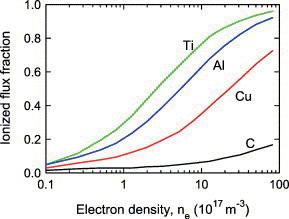
54
55
56
57
58
59
60
61
62
63
64
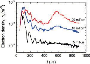
65
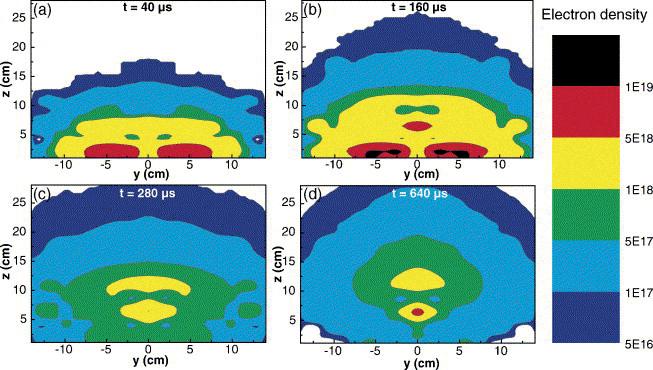
66
67
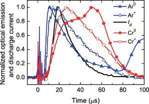
68
69
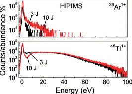
70
71
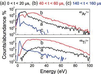
72
73
74
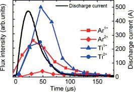
75
76
77
78
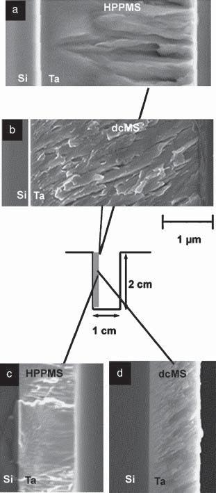
79
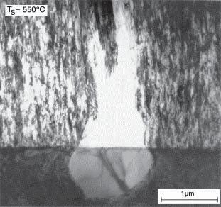
80
A novel sputtering technique: Inductively Coupled Impulse Sputtering (ICIS)
") IOP Conference Series: Materials Science and Engineering A novel sputtering technique: Inductively Coupled Impulse Sputtering (ICIS) To cite this article: D A L Loch and A P Ehiasarian 2012 IOP Conf. Ser.:
IOP Conference Series: Materials Science and Engineering A novel sputtering technique: Inductively Coupled Impulse Sputtering (ICIS) To cite this article: D A L Loch and A P Ehiasarian 2012 IOP Conf. Ser.:
DEPOSITION OF THIN TiO 2 FILMS BY DC MAGNETRON SPUTTERING METHOD
 Chapter 4 DEPOSITION OF THIN TiO 2 FILMS BY DC MAGNETRON SPUTTERING METHOD 4.1 INTRODUCTION Sputter deposition process is another old technique being used in modern semiconductor industries. Sputtering
PRINCIPLES OF PLASMA DISCHARGES AND MATERIALS PROCESSING
 PRINCIPLES OF PLASMA DISCHARGES AND MATERIALS PROCESSING Second Edition MICHAEL A. LIEBERMAN ALLAN J, LICHTENBERG WILEY- INTERSCIENCE A JOHN WILEY & SONS, INC PUBLICATION CONTENTS PREFACE xrrii PREFACE
Hysteresis-free reactive high power impulse magnetron sputtering
 Linköping University Postprint Hysteresis-free reactive high power impulse magnetron sputtering E. Wallin and U. Helmersson N.B.: When citing this work, cite the original article. Original publication:
The role of recycling in pulsed sputtering magnetrons
 The role of recycling in pulsed sputtering magnetrons Jón Tómas Guðmundsson 1,2,3, Daniel Lundin 3, Michael A. Raadu 1, Thomas J. Petty 3, Tiberiu M. Minea 3, and Nils Brenning 1 1 Department of Space
SCALING OF HOLLOW CATHODE MAGNETRONS FOR METAL DEPOSITION a)
") SCALING OF HOLLOW CATHODE MAGNETRONS FOR METAL DEPOSITION a) Gabriel Font b) Novellus Systems, Inc. San Jose, CA, 95134 USA and Mark J. Kushner Dept. of Electrical and Computer Engineering Urbana, IL,
SCALING OF HOLLOW CATHODE MAGNETRONS FOR METAL DEPOSITION a) Gabriel Font b) Novellus Systems, Inc. San Jose, CA, 95134 USA and Mark J. Kushner Dept. of Electrical and Computer Engineering Urbana, IL,
Robert A. Meger Richard F. Fernster Martin Lampe W. M. Manheimer NOTICE
 Serial Number Filing Date Inventor 917.963 27 August 1997 Robert A. Meger Richard F. Fernster Martin Lampe W. M. Manheimer NOTICE The above identified patent application is available for licensing. Requests
Chapter 7 Plasma Basic
 Chapter 7 Plasma Basic Hong Xiao, Ph. D. hxiao89@hotmail.com www2.austin.cc.tx.us/hongxiao/book.htm Hong Xiao, Ph. D. www2.austin.cc.tx.us/hongxiao/book.htm 1 Objectives List at least three IC processes
MICROCHIP MANUFACTURING by S. Wolf
 by S. Wolf Chapter 15 ALUMINUM THIN-FILMS and SPUTTER-DEPOSITION 2004 by LATTICE PRESS CHAPTER 15 - CONTENTS Aluminum Thin-Films Sputter-Deposition Process Steps Physics of Sputter-Deposition Magnetron-Sputtering
Huashun Zhang. Ion Sources. With 187 Figures and 26 Tables Э SCIENCE PRESS. Springer
 Huashun Zhang Ion Sources With 187 Figures and 26 Tables Э SCIENCE PRESS Springer XI Contents 1 INTRODUCTION 1 1.1 Major Applications and Requirements 1 1.2 Performances and Research Subjects 1 1.3 Historical
Plasma Modeling with COMSOL Multiphysics
 Plasma Modeling with COMSOL Multiphysics Copyright 2014 COMSOL. Any of the images, text, and equations here may be copied and modified for your own internal use. All trademarks are the property of their
Repetition: Practical Aspects
 Repetition: Practical Aspects Reduction of the Cathode Dark Space! E x 0 Geometric limit of the extension of a sputter plant. Lowest distance between target and substrate V Cathode (Target/Source) - +
Chapter VI: Cold plasma generation
 Introduction This photo shows the electrical discharge inside a highpressure mercury vapor lamp (Philips HO 50) just after ignition (Hg + Ar) Chapter VI: Cold plasma generation Anode Positive column Cathode
Chapter 7. Plasma Basics
 Chapter 7 Plasma Basics 2006/4/12 1 Objectives List at least three IC processes using plasma Name three important collisions in plasma Describe mean free path Explain how plasma enhance etch and CVD processes
6.5 Optical-Coating-Deposition Technologies
 92 Chapter 6 6.5 Optical-Coating-Deposition Technologies The coating process takes place in an evaporation chamber with a fully controlled system for the specified requirements. Typical systems are depicted
Plasma diagnostics of pulsed sputtering discharge
 Plasma diagnostics of pulsed sputtering discharge Vitezslav Stranak Zdenek Hubicka, Martin Cada and Rainer Hippler University of Greifswald, Institute of Physics, Felix-Hausdorff-Str. 6, 174 89 Greifswald,
Etching Issues - Anisotropy. Dry Etching. Dry Etching Overview. Etching Issues - Selectivity
 Etching Issues - Anisotropy Dry Etching Dr. Bruce K. Gale Fundamentals of Micromachining BIOEN 6421 EL EN 5221 and 6221 ME EN 5960 and 6960 Isotropic etchants etch at the same rate in every direction mask
Unit-2 LASER. Syllabus: Properties of lasers, types of lasers, derivation of Einstein A & B Coefficients, Working He-Ne and Ruby lasers.
 Unit-2 LASER Syllabus: Properties of lasers, types of lasers, derivation of Einstein A & B Coefficients, Working He-Ne and Ruby lasers. Page 1 LASER: The word LASER is acronym for light amplification by
SPUTTER-WIND HEATING IN IONIZED METAL PVD+
 SPUTTER-WIND HEATING IN IONIZED METAL PVD+ Junqing Lu* and Mark Kushner** *Department of Mechanical and Industrial Engineering **Department of Electrical and Computer Engineering University of Illinois
Keywords. 1=magnetron sputtering, 2= rotatable cathodes, 3=substrate temperature, 4=anode. Abstract
 Managing Anode Effects and Substrate Heating from Rotatable Sputter Targets. F. Papa*, V. Bellido-Gonzalez**, Alex Azzopardi**, Dr. Dermot Monaghan**, *Gencoa Technical & Business Support in US, Davis,
E SC 412 Nanotechnology: Materials, Infrastructure, and Safety Wook Jun Nam
 E SC 412 Nanotechnology: Materials, Infrastructure, and Safety Wook Jun Nam Lecture 10 Outline 1. Wet Etching/Vapor Phase Etching 2. Dry Etching DC/RF Plasma Plasma Reactors Materials/Gases Etching Parameters
TMT4320 Nanomaterials November 10 th, Thin films by physical/chemical methods (From chapter 24 and 25)
") 1 TMT4320 Nanomaterials November 10 th, 2015 Thin films by physical/chemical methods (From chapter 24 and 25) 2 Thin films by physical/chemical methods Vapor-phase growth (compared to liquid-phase growth)
1 TMT4320 Nanomaterials November 10 th, 2015 Thin films by physical/chemical methods (From chapter 24 and 25) 2 Thin films by physical/chemical methods Vapor-phase growth (compared to liquid-phase growth)
Linköping University Post Print. Cross-field ion transport during high power impulse magnetron sputtering
 Linköping University Post Print Cross-field ion transport during high power impulse magnetron sputtering Daniel Lundin, Petter Larsson, Erik Wallin, Martina Lattemann, Nils Brenning and Ulf Helmersson
ETCHING Chapter 10. Mask. Photoresist
 ETCHING Chapter 10 Mask Light Deposited Substrate Photoresist Etch mask deposition Photoresist application Exposure Development Etching Resist removal Etching of thin films and sometimes the silicon substrate
Characteristics and classification of plasmas
 Characteristics and classification of plasmas PlasTEP trainings course and Summer school 2011 Warsaw/Szczecin Indrek Jõgi, University of Tartu Partfinanced by the European Union (European Regional Development
MODELING OF AN ECR SOURCE FOR MATERIALS PROCESSING USING A TWO DIMENSIONAL HYBRID PLASMA EQUIPMENT MODEL. Ron L. Kinder and Mark J.
 TECHCON 98 Las Vegas, Nevada September 9-11, 1998 MODELING OF AN ECR SOURCE FOR MATERIALS PROCESSING USING A TWO DIMENSIONAL HYBRID PLASMA EQUIPMENT MODEL Ron L. Kinder and Mark J. Kushner Department of
ELEMENT2 High Resolution- ICP-MS INSTRUMENT OVERVIEW
 ELEMENT2 High Resolution- ICP-MS INSTRUMENT OVERVIEW Inductively Coupled Plasma Mass Spectrometry (ICP-MS) What is a Plasma? - The magnetic field created by a RF (radio frequency) coil produces
Introduction to Plasma
 What is a plasma? The fourth state of matter A partially ionized gas How is a plasma created? Energy must be added to a gas in the form of: Heat: Temperatures must be in excess of 4000 O C Radiation Electric
A strategy for increased carbon ionization in magnetron sputtering discharges
 A strategy for increased carbon ionization in magnetron sputtering discharges Asim Aijaz, Kostas Sarakinos, Daniel Lundin, Nils Brenning and Ulf Helmersson Linköping University Post Print N.B.: When citing
Study of DC Cylindrical Magnetron by Langmuir Probe
 WDS'2 Proceedings of Contributed Papers, Part II, 76 8, 22. ISBN 978-737825 MATFYZPRESS Study of DC Cylindrical Magnetron by Langmuir Probe A. Kolpaková, P. Kudrna, and M. Tichý Charles University Prague,
The Q Machine. 60 cm 198 cm Oven. Plasma. 6 cm 30 cm. 50 cm. Axial. Probe. PUMP End Plate Magnet Coil. Filament Cathode. Radial. Hot Plate.
 1 The Q Machine 60 cm 198 cm Oven 50 cm Axial Probe Plasma 6 cm 30 cm PUMP End Plate Magnet Coil Radial Probe Hot Plate Filament Cathode 2 THE Q MACHINE 1. GENERAL CHARACTERISTICS OF A Q MACHINE A Q machine
Metal Deposition. Filament Evaporation E-beam Evaporation Sputter Deposition
 Metal Deposition Filament Evaporation E-beam Evaporation Sputter Deposition 1 Filament evaporation metals are raised to their melting point by resistive heating under vacuum metal pellets are placed on
Exploration into Sputtered ITO Film Properties as a Function of Magnetic Field Strength
 Tangential Magnetic Flux, Gauss Exploration into Sputtered ITO Film Properties as a Function of Magnetic Field Strength Patrick Morse and Timmy Strait Sputtering Components Inc. Owatonna Minnesota ABSTRACT
Dense plasma formation on the surface of a ferroelectric cathode
 Vacuum ] (]]]]) ]]] ]]] www.elsevier.com/locate/vacuum Dense plasma formation on the surface of a ferroelectric cathode K. Chirko, Ya.E. Krasik, A. Sayapin, J. Felsteiner Physics Department, Technion Israel
Lecture 6 Plasmas. Chapters 10 &16 Wolf and Tauber. ECE611 / CHE611 Electronic Materials Processing Fall John Labram 1/68
 Lecture 6 Plasmas Chapters 10 &16 Wolf and Tauber 1/68 Announcements Homework: Homework will be returned to you on Thursday (12 th October). Solutions will be also posted online on Thursday (12 th October)
PH2200 Practice Final Exam Summer 2003
 INSTRUCTIONS 1. Write your name and student identification number on the answer sheet. 2. Please cover your answer sheet at all times. 3. This is a closed book exam. You may use the PH2200 formula sheet
This is an author produced version of a paper presented at 2nd PATCMC, June 6th-8th 2011 Plzeň, Czech Republic.
 http://uu.diva-portal.org This is an author produced version of a paper presented at 2nd PATCMC, June 6th-8th 2011 Plzeň, Czech Republic. Kubart, T. 2011. Process modelling for reactive magnetron sputtering
Effect of Spiral Microwave Antenna Configuration on the Production of Nano-crystalline Film by Chemical Sputtering in ECR Plasma
 THE HARRIS SCIENCE REVIEW OF DOSHISHA UNIVERSITY, VOL. 56, No. 1 April 2015 Effect of Spiral Microwave Antenna Configuration on the Production of Nano-crystalline Film by Chemical Sputtering in ECR Plasma
Measurement of electron energy distribution function in an argon/copper plasma for ionized physical vapor deposition
 Measurement of electron energy distribution function in an argon/copper plasma for ionized physical vapor deposition Z. C. Lu, J. E. Foster, T. G. Snodgrass, J. H. Booske, and A. E. Wendt a) Engineering
PIC/MCC Simulation of Radio Frequency Hollow Cathode Discharge in Nitrogen
 PIC/MCC Simulation of Radio Frequency Hollow Cathode Discharge in Nitrogen HAN Qing ( ), WANG Jing ( ), ZHANG Lianzhu ( ) College of Physics Science and Information Engineering, Hebei Normal University,
Plasma Deposition (Overview) Lecture 1
 Lecture 1") Plasma Deposition (Overview) Lecture 1 Material Processes Plasma Processing Plasma-assisted Deposition Implantation Surface Modification Development of Plasma-based processing Microelectronics needs (fabrication
Plasma Deposition (Overview) Lecture 1 Material Processes Plasma Processing Plasma-assisted Deposition Implantation Surface Modification Development of Plasma-based processing Microelectronics needs (fabrication
- A spark is passed through the Argon in the presence of the RF field of the coil to initiate the plasma
 THE PLASMA Inductively Coupled Plasma Mass Spectrometry (ICP-MS) What is a Plasma? - The magnetic field created by a RF (radio frequency) coil produces a current within a stream of Argon (Ar) gas, which
INTRODUCTION TO THE HYBRID PLASMA EQUIPMENT MODEL
 INTRODUCTION TO THE HYBRID PLASMA EQUIPMENT MODEL Prof. Mark J. Kushner Department of Electrical and Computer Engineering 1406 W. Green St. Urbana, IL 61801 217-144-5137 mjk@uiuc.edu http://uigelz.ece.uiuc.edu
June 5, 2012: Did you miss it? No Problem. Next chance in Venus in Front of the Sun and there is more: plasma imaging!
 July 18 20, 2012 5th Int. Workshop on "Thin Films Applied To Superconducting RF And New Ideas For Pushing The Limits Of RF Superconductivity" Jefferson Lab, VA Strong localization of ionization in high
Hiden EQP Applications
 Hiden EQP Applications Mass/Energy Analyser for Plasma Diagnostics and Characterisation EQP Overview The Hiden EQP System is an advanced plasma diagnostic tool with combined high transmission ion energy
arxiv: v1 [physics.plasm-ph] 10 Nov 2014
![arxiv: v1 [physics.plasm-ph] 10 Nov 2014](/thumbs/88/117240344.jpg "arxiv: v1 [physics.plasm-ph] 10 Nov 2014") arxiv:1411.2464v1 [physics.plasm-ph] 10 Nov 2014 Effects of fast atoms and energy-dependent secondary electron emission yields in PIC/MCC simulations of capacitively coupled plasmas A. Derzsi 1, I. Korolov
arxiv:1411.2464v1 [physics.plasm-ph] 10 Nov 2014 Effects of fast atoms and energy-dependent secondary electron emission yields in PIC/MCC simulations of capacitively coupled plasmas A. Derzsi 1, I. Korolov
CHAPTER 6: Etching. Chapter 6 1
 Chapter 6 1 CHAPTER 6: Etching Different etching processes are selected depending upon the particular material to be removed. As shown in Figure 6.1, wet chemical processes result in isotropic etching
PHYSICAL VAPOR DEPOSITION OF THIN FILMS
 PHYSICAL VAPOR DEPOSITION OF THIN FILMS JOHN E. MAHAN Colorado State University A Wiley-Interscience Publication JOHN WILEY & SONS, INC. New York Chichester Weinheim Brisbane Singapore Toronto CONTENTS
Combinatorial RF Magnetron Sputtering for Rapid Materials Discovery: Methodology and Applications
 Combinatorial RF Magnetron Sputtering for Rapid Materials Discovery: Methodology and Applications Philip D. Rack,, Jason D. Fowlkes,, and Yuepeng Deng Department of Materials Science and Engineering University
Hong Young Chang Department of Physics, Korea Advanced Institute of Science and Technology (KAIST), Republic of Korea
, Republic of Korea") Hong Young Chang Department of Physics, Korea Advanced Institute of Science and Technology (KAIST), Republic of Korea Index 1. Introduction 2. Some plasma sources 3. Related issues 4. Summary -2 Why is
Hong Young Chang Department of Physics, Korea Advanced Institute of Science and Technology (KAIST), Republic of Korea Index 1. Introduction 2. Some plasma sources 3. Related issues 4. Summary -2 Why is
Electron Temperature Modification in Gas Discharge Plasma
 Electron Temperature Modification in Gas Discharge Plasma Valery Godyak University of Michigan and RF Plasma Consulting egodyak@comcast.net Workshop: Control of Distribution Functions in Low Temperature
Physique des plasmas radiofréquence Pascal Chabert
 Physique des plasmas radiofréquence Pascal Chabert LPP, Ecole Polytechnique pascal.chabert@lpp.polytechnique.fr Planning trois cours : Lundi 30 Janvier: Rappels de physique des plasmas froids Lundi 6 Février:
Mass Analyzers. Principles of the three most common types magnetic sector, quadrupole and time of flight - will be discussed herein.
 Mass Analyzers After the production of ions in ion sources, the next critical step in mass spectrometry is to separate these gas phase ions according to their mass-to-charge ratio (m/z). Ions are extracted
Plasma Processing in the Microelectronics Industry. Bert Ellingboe Plasma Research Laboratory
 Plasma Processing in the Microelectronics Industry Bert Ellingboe Plasma Research Laboratory Outline What has changed in the last 12 years? What is the relavant plasma physics? Sheath formation Sheath
Theory of Gas Discharge
 Boris M. Smirnov Theory of Gas Discharge Plasma l Springer Contents 1 Introduction 1 Part I Processes in Gas Discharge Plasma 2 Properties of Gas Discharge Plasma 13 2.1 Equilibria and Distributions of
Dynamization evolution of Dry Etch Tools in Semiconductor Device Fabrication Gordon Cameron Intel Corp (November 2005)
") Dynamization evolution of Dry Etch Tools in Semiconductor Device Fabrication Gordon Cameron Intel Corp (November 2005) Abstract Engineering Systems follow recognized trends of evolution; the main parameters
Dynamization evolution of Dry Etch Tools in Semiconductor Device Fabrication Gordon Cameron Intel Corp (November 2005) Abstract Engineering Systems follow recognized trends of evolution; the main parameters
Secondary Ion Mass Spectroscopy (SIMS)
") Secondary Ion Mass Spectroscopy (SIMS) Analyzing Inorganic Solids * = under special conditions ** = semiconductors only + = limited number of elements or groups Analyzing Organic Solids * = under special
Secondary Ion Mass Spectroscopy (SIMS) Analyzing Inorganic Solids * = under special conditions ** = semiconductors only + = limited number of elements or groups Analyzing Organic Solids * = under special
Cesium Dynamics and H - Density in the Extended Boundary Layer of Negative Hydrogen Ion Sources for Fusion
 Cesium Dynamics and H - Density in the Extended Boundary Layer of Negative Hydrogen Ion Sources for Fusion C. Wimmer a, U. Fantz a,b and the NNBI-Team a a Max-Planck-Institut für Plasmaphysik, EURATOM
Introduction to Thin Film Processing
 Introduction to Thin Film Processing Deposition Methods Many diverse techniques available Typically based on three different methods for providing a flux of atomic or molecular material Evaporation Sputtering
ELECTROMAGNETIC WAVES
 VISUAL PHYSICS ONLINE MODULE 7 NATURE OF LIGHT ELECTROMAGNETIC WAVES SPECTRA PRODUCED BY DISCHARGE TUBES CATHODE RAYS (electron beams) Streams of electrons (negatively charged particles) observed in vacuum
Langmuir Probes as a Diagnostic to Study Plasma Parameter Dependancies, and Ion Acoustic Wave Propogation
 Langmuir Probes as a Diagnostic to Study Plasma Parameter Dependancies, and Ion Acoustic Wave Propogation Kent Lee, Dean Henze, Patrick Smith, and Janet Chao University of San Diego (Dated: May 1, 2013)
The effect of self-absorption in hollow cathode lamp on its temperature
 Plasma Science and Applications (ICPSA 2013) International Journal of Modern Physics: Conference Series Vol. 32 (2014) 1460349 (9 pages) The Author DOI: 10.1142/S2010194514603494 The effect of self-absorption
high temp ( K) Chapter 20: Atomic Spectroscopy
 Chapter 20: Atomic Spectroscopy") high temp (2000-6000K) Chapter 20: Atomic Spectroscopy 20-1. An Overview Most compounds Atoms in gas phase high temp (2000-6000K) (AES) (AAS) (AFS) sample Mass-to-charge (ICP-MS) Atomic Absorption experiment
high temp (2000-6000K) Chapter 20: Atomic Spectroscopy 20-1. An Overview Most compounds Atoms in gas phase high temp (2000-6000K) (AES) (AAS) (AFS) sample Mass-to-charge (ICP-MS) Atomic Absorption experiment
FLASH CHAMBER OF A QUASI-CONTINUOUS VOLUME SOURCE OF NEGATIVE IONS
 FLASH CHAMBER OF A QUASI-CONTINUOUS VOLUME SOURCE OF NEGATIVE IONS P.A. Litvinov, V.A. Baturin * Institute of Applied Physics, National Academy of Science of Ukraine, 58 Petropavlovskaya St. Sumy, 40030
ICPMS Doherty Lecture 1
 ICPMS Doherty Lecture 1 Mass Spectrometry This material provides some background on how to measure isotope abundances by means of mass spectrometry. Mass spectrometers create and separate ionized atoms
Experiments with a Supported Dipole
 Experiments with a Supported Dipole Reporting Measurements of the Interchange Instability Excited by Electron Pressure and Centrifugal Force Introduction Ben Levitt and Dmitry Maslovsky Collisionless Terrella
CHARACTERIZATION OF A DC PLASMA WITH HOLLOW CATHODE EFFECT
 Romanian Reports in Phisics, Vol. 56, No., P. 71-76, 004 CHARACTERIZATION OF A DC PLASMA WITH HOLLOW CATHODE EFFECT A. R. PETRE 1, M. BÃZÃVAN 1, V. COVLEA 1, V.V. COVLEA 1, ISABELLA IOANA OPREA, H. ANDREI
SIMULATIONS OF ECR PROCESSING SYSTEMS SUSTAINED BY AZIMUTHAL MICROWAVE TE(0,n) MODES*
 MODES*") 25th IEEE International Conference on Plasma Science Raleigh, North Carolina June 1-4, 1998 SIMULATIONS OF ECR PROCESSING SYSTEMS SUSTAINED BY AZIMUTHAL MICROWAVE TE(,n) MODES* Ron L. Kinder and Mark J.
25th IEEE International Conference on Plasma Science Raleigh, North Carolina June 1-4, 1998 SIMULATIONS OF ECR PROCESSING SYSTEMS SUSTAINED BY AZIMUTHAL MICROWAVE TE(,n) MODES* Ron L. Kinder and Mark J.
Electrical Discharges Characterization of Planar Sputtering System
 International Journal of Recent Research and Review, Vol. V, March 213 ISSN 2277 8322 Electrical Discharges Characterization of Planar Sputtering System Bahaa T. Chaid 1, Nathera Abass Ali Al-Tememee 2,
Electron temperature is the temperature that describes, through Maxwell's law, the kinetic energy distribution of the free electrons.
 10.3.1.1 Excitation and radiation of spectra 10.3.1.1.1 Plasmas A plasma of the type occurring in spectrochemical radiation sources may be described as a gas which is at least partly ionized and contains
High power impulse magnetron sputtering (HIPIMS) : Fundamental plasma studies and material synthesis.
 : Fundamental plasma studies and material synthesis.") High power impulse magnetron sputtering (HIPIMS) : Fundamental plasma studies and material synthesis. HECIMOVIC, Ante. Available from Sheffield Hallam University Research Archive (SHURA) at: http://shura.shu.ac.uk/19781/
High power impulse magnetron sputtering (HIPIMS) : Fundamental plasma studies and material synthesis. HECIMOVIC, Ante. Available from Sheffield Hallam University Research Archive (SHURA) at: http://shura.shu.ac.uk/19781/
XXXXXXXXXXXXXXX. First Pre-Board Examination, Physics
 Series SSO Code No. 55/1/B Roll No. Candidates must write the code on the title page of the answer book General Instructions: Please check that this question paper contains 6 printed pages. Code number
Stepwise Solution Important Instructions to examiners:
 (ISO/IEC - 700-005 Certified) SUMMER 05 EXAMINATION Subject Code: 70 Model Answer (Applied Science- Physics) Page No: 0/6 Que. No. Sub. Que. Important Instructions to examiners: ) The answers should be
MONOCHROMATIZATION AND POLARIZATION OF THE NEON SPECTRAL LINES IN CONSTANT/VARIABLE MAGNETIC FIELD
 Romanian Reports in Physics 69, 49 (217) MONOCHROMATIZATION AND POLARIZATION OF THE NEON SPECTRAL LINES IN CONSTANT/VARIABLE MAGNETIC FIELD I. GRUIA, L.C. CIOBOTARU* University of Bucharest, Faculty of
MODELING AND SIMULATION OF LOW TEMPERATURE PLASMA DISCHARGES
 MODELING AND SIMULATION OF LOW TEMPERATURE PLASMA DISCHARGES Michael A. Lieberman University of California, Berkeley lieber@eecs.berkeley.edu DOE Center on Annual Meeting May 2015 Download this talk: http://www.eecs.berkeley.edu/~lieber
arxiv: v1 [physics.plasm-ph] 23 May 2013
![arxiv: v1 [physics.plasm-ph] 23 May 2013](/thumbs/89/99068732.jpg "arxiv: v1 [physics.plasm-ph] 23 May 2013") The characteristic shape of emission profiles of plasma spokes in HiPIMS: the role of secondary electrons A. Hecimovic 1, S. Gallian 2, R.-P. Brinkmann 2, M. Böke 1, J. Winter 1 1 Institute of Experimental
The characteristic shape of emission profiles of plasma spokes in HiPIMS: the role of secondary electrons A. Hecimovic 1, S. Gallian 2, R.-P. Brinkmann 2, M. Böke 1, J. Winter 1 1 Institute of Experimental
Ionization Techniques Part IV
 Ionization Techniques Part IV CU- Boulder CHEM 5181 Mass Spectrometry & Chromatography Presented by Prof. Jose L. Jimenez High Vacuum MS Interpretation Lectures Sample Inlet Ion Source Mass Analyzer Detector
FINAL REPORT. DOE Grant DE-FG03-87ER13727
 FINAL REPORT DOE Grant DE-FG03-87ER13727 Dynamics of Electronegative Plasmas for Materials Processing Allan J. Lichtenberg and Michael A. Lieberman Department of Electrical Engineering and Computer Sciences
Electromagnetics in COMSOL Multiphysics is extended by add-on Modules
 AC/DC Module Electromagnetics in COMSOL Multiphysics is extended by add-on Modules 1) Start Here 2) Add Modules based upon your needs 3) Additional Modules extend the physics you can address 4) Interface
The Franck-Hertz Experiment Physics 2150 Experiment No. 9 University of Colorado
 Experiment 9 1 Introduction The Franck-Hertz Experiment Physics 2150 Experiment No. 9 University of Colorado During the late nineteenth century, a great deal of evidence accumulated indicating that radiation
Vacuum Pumps. Two general classes exist: Gas transfer physical removal of matter. Mechanical, diffusion, turbomolecular
 Vacuum Technology Vacuum Pumps Two general classes exist: Gas transfer physical removal of matter Mechanical, diffusion, turbomolecular Adsorption entrapment of matter Cryo, sublimation, ion Mechanical
Electron cyclotron resonance plasma enhanced direct current sputtering discharge with magnetic-mirror plasma confinement
 Electron cyclotron resonance plasma enhanced direct current sputtering discharge with magnetic-mirror plasma confinement M. Mišina, a) Y. Setsuhara, and S. Miyake Joining and Welding Research Institute,
Chemistry Instrumental Analysis Lecture 17. Chem 4631
 Chemistry 4631 Instrumental Analysis Lecture 17 Introduction to Optical Atomic Spectrometry From molecular to elemental analysis there are three major techniques used for elemental analysis: Optical spectrometry
Miniature Vacuum Arc Thruster with Controlled Cathode Feeding
 Miniature Vacuum Arc Thruster with Controlled Cathode Feeding Igal Kronhaus and Matteo Laterza Aerospace Plasma Laboratory, Faculty of Aerospace Engineering, Technion - Israel Institute of Technology,
Large Plasma Device (LAPD)
") Large Plasma Device (LAPD) Over 450 Access ports Computer Controlled Data Acquisition Microwave Interferometers Laser Induced Fluorescence DC Magnetic Field: 0.05-4 kg, variable on axis Highly Ionized
Large Plasma Device (LAPD) Over 450 Access ports Computer Controlled Data Acquisition Microwave Interferometers Laser Induced Fluorescence DC Magnetic Field: 0.05-4 kg, variable on axis Highly Ionized
High Power Impulse Magnetron Sputtering for Industrial Applications: Deposition of Chromium Films on Inclined Surfaces
 High Power Impulse Magnetron Sputtering for Industrial Applications: Deposition of Chromium Films on Inclined Surfaces Grzegorz Greczynski and Johan Böhlmark, Chemfilt Ionsputtering AB, Linköping, Sweden;
Table of Content. Mechanical Removing Techniques. Ultrasonic Machining (USM) Sputtering and Focused Ion Beam Milling (FIB)
 Sputtering and Focused Ion Beam Milling (FIB)") Table of Content Mechanical Removing Techniques Ultrasonic Machining (USM) Sputtering and Focused Ion Beam Milling (FIB) Ultrasonic Machining In ultrasonic machining (USM), also called ultrasonic grinding,
Table of Content Mechanical Removing Techniques Ultrasonic Machining (USM) Sputtering and Focused Ion Beam Milling (FIB) Ultrasonic Machining In ultrasonic machining (USM), also called ultrasonic grinding,
Modélisation particulaire du plasma magnétron impulsionnel haute puissance
 Modélisation particulaire du plasma magnétron impulsionnel haute puissance Tiberiu MINEA Laboratoire de Physique des Gaz et Plasmas LPGP UMR 8578 CNRS, Université Paris-Sud, 91405 Orsay Cedex, France tiberiu.minea@u-psud.fr
Beams and magnetized plasmas
 Beams and magnetized plasmas 1 Jean-Pierre BOEUF LAboratoire PLAsma et Conversion d Energie LAPLACE/ CNRS, Université Paul SABATIER, TOULOUSE Beams and magnetized plasmas 2 Outline Ion acceleration and
Composition and dynamics of high power impulse magnetron discharge at W-Mo-C target in argon atmosphere
 Composition and dynamics of high power impulse magnetron discharge at W-Mo-C target in argon atmosphere GAJEWSKI, W., EHIASARIAN, A.P. , ŻELECHOWSKI, M. and HOVSEPIAN,
Extrel Application Note
 Extrel Application Note Real-Time Plasma Monitoring and Detection of Trace H 2 O and HF Species in an Argon Based Plasma Jian Wei, 575 Epsilon Drive, Pittsburgh, PA 15238. (Presented at the 191st Electrochemical
Adjustment of electron temperature in ECR microwave plasma
 Vacuum (3) 53 Adjustment of electron temperature in ECR microwave plasma Ru-Juan Zhan a, Xiaohui Wen a,b, *, Xiaodong Zhu a,b, Aidi zhao a,b a Structure Research Laboratory, University of Science and Technology
High power impulse plasmas for thin film deposition
 High power impulse plasmas for thin film deposition Fortgeschrittenen-Praktikum Ruhr-Universität Bochum Ante Hecimovic 23 March, 2012 The Electrostatic Quadrupole Plasma (EQP) Mass Spectrometer is an experimental
1P22/1P92 Exam Review Problems 2013 Friday, January 14, :03 AM. Chapter 20
 Exam Review Problems 2011 Page 1 1P22/1P92 Exam Review Problems 2013 Friday, January 14, 2011 10:03 AM Chapter 20 True or false? 1 It's impossible to place a charge on an insulator, because no current
vacuum analysis plasma diagnostics surface science gas analysis
 Hiden EQP Systems High Sensitivity Mass and Energy Analysers for Monitoring, Control and Characterisation of Ions, Neutrals and Radicals in Plasma. vacuum analysis surface science gas analysis plasma diagnostics
Previous Lecture. Electron beam lithoghraphy e - Electrons are generated in vacuum. Electron beams propagate in vacuum
 Previous Lecture Electron beam lithoghraphy e - Electrons are generated in vacuum Electron beams propagate in vacuum Lecture 6: Vacuum & plasmas Objectives From this vacuum lecture you will learn: What
Neutral beam plasma heating
 Seminar I b 1 st year, 2 nd cycle program Neutral beam plasma heating Author: Gabrijela Ikovic Advisor: prof.dr. Tomaž Gyergyek Ljubljana, May 2014 Abstract For plasma to be ignited, external heating is
a. An emission line as close as possible to the analyte resonance line
 Practice Problem Set 5 Atomic Emission Spectroscopy 10-1 What is an internal standard and why is it used? An internal standard is a substance added to samples, blank, and standards. The ratio of the signal
Some Reflections on Gas Discharges and PAGD Pulses
 Some Reflections on Gas Discharges and PAGD Pulses By William A. Tiller A typical graph relating the voltage difference, V a, between parallel planar electrodes and the discharge current, i, in a gas discharge
Interface (backside) & Extraction Lens
 & Extraction Lens") Plasma Interface Interface (backside) & Extraction Lens Extraction Lens (-2000 volts) ION OPTICS Tip of the sampler cone is positioned to be in the region of maximum ionization Ions no longer under control
Plasma Interface Interface (backside) & Extraction Lens Extraction Lens (-2000 volts) ION OPTICS Tip of the sampler cone is positioned to be in the region of maximum ionization Ions no longer under control